Note: Descriptions are shown in the official language in which they were submitted.
CA 02539269 2006-03-16
WO 2005/031326 PCT/SE2004/001375
1
SYSTEM AND METHOD OF IMAGING THE CHARACTERISTICS OF AN OB7ECT
BACKGROUND OF THE INVENTION
Field of the Invention
[0001] The present patent application relates to the field of imaging the
characteristics of
an object, and particularly to a measuring system allowing for detecting
defects of an
object by imaging the characteristics of the object having at least a first
and a second
layer as well as a method for such detection.
Description of the Related Art
[0002] Quality control is very important in for instance the packaging
industry. Most
manufacturers perform a manual visual inspection of the products, i.e.
examining the
products with the human eye. This is time consuming, expensive, not very
efficient and
may be considered to be a subjective evaluation. An alternative to the manual
quality
inspection is to use an automated inspection system. However, the inspection
of
transparent or semi-transparent materials is difficult since defects on these
materials are
invisible to normal inspection systems.
[0003] One method of inspecting transparent objects, such as glass or
plastics, is to use a
bright-field/dark-field system. The bright-field is the region where specular
reflected light
from the object is imaged on a sensor. The dark-held is the region in which
diffusely
reflected light from the object is imaged on a sensor. The signals from the
dark- and bright-
field sensors can be used to detect defects on the surface of transparent
objects. When no
defect is present, the bright-field image is bright and the dark-field image
is dark. But,
when the object has a defect, the dark-field image presents an increased
brightness.
However, this method of inspecting transparent objects only detects defects on
a surface
layer.
[0004] One prior art approach is disclosed in EP 902 275, which suggests an
imaging
apparatus and process for inspecting an object wrapped in a transparent or
semi-
transparent material, such as a cigarette package wrapped in a polymeric film.
Incident
fight is directed upon the object such that the light enters the wrapper and
the wrapper
acts as a waveguide. The light escapes from the poly film wrap at edges and
folds where
it reaches a reflective boundary. The escaped light is captured by a camera
and is
CA 02539269 2006-03-16
WO 2005/031326 PCT/SE2004/001375
thereafter sent to an imaging processor. Thus, overwrap defects, such as
misplacement,
misfolding, tearing, wrinkling or other defects, will be detected.
[0005] However, this prior art approach only detects defects in a wrapping
layer. Defects
on the package itself must be separately inspected at a separate stage
requiring more
than one inspection system, manual or automatic.
[0006] Therefore, there is a need for a system and a method for the detection
of defects
on an object comprising at least two layers, where at least the first layer
consists of a
transparent or semi-transparent material.
SUMMARY OF THE INVENTION
[0007] Accordingly, it is an object of the present invention to provide an
improved
measuring system allowing for imaging the characteristics of an object having
at least a
first and a second layer.
[0008] This object is achieved through providing a measuring system comprising
at least
one light source arranged to illuminate the object with incident light, an
imaging sensor
arranged to detect reflected light from the object and to convert the detected
light into
electrical charges and, means for creating a representation of the object
according to the
electrical charges, wherein the device comprises means for obtaining
information on light
scattered in the first layer and the second layer of the object from the
representation
and, means for comparing the information to stored information in order to
detect
defects on the object.
[0009] Another object of the invention is to provide an improved method for
imaging the
characteristics of an object having at least a first and a second layer.
[0010] This object is achieved through a method of providing a measuring
system, in
which the object is illuminated by means of incident light, and light
reflected from the
object is detected by means of an imaging sensor in which the detected light
is converted
into electrical charges, according to which a representation of the object is
created,
whereby information on light scattered in at least a first layer and a second
layer of the
object is obtained from the representation and that the information is
compared to stored
information in order to detect defects on the object.
CA 02539269 2006-03-16
WO 2005/031326 PCT/SE2004/001375
3
[0011] Still other objects and features of the present invention will become
apparent
from the following detailed description considered in conjunction with the
accompanying
drawings. It is to be understood, however, that the drawings are designed
solely for
purposes of illustration and not as a definition of the limits of the
invention, for which
reference should be made to the appended claims. It should be further
understood that
the drawings are not necessarily drawn to scale and that, unless otherwise
indicated,
they are merely intended to conceptually illustrate the structures and
procedures
described herein.
BRIEF DESCRIPTION OF THE DRAWINGS
[0012] In the drawings, wherein like reference characters denote similar
elements
throughout the several views:
[0013] Fig. 1 discloses a schematic view of a measuring system according to a
first
embodiment of the invention;
[0014] Fig. 2a discloses a view of an object to be examined showing how light
normally
scatters in the different layers in a first example of how d efects are
detected and
classified with the inventive system;
[0015] Fig 2b discloses how light scatters when a second layer of an object to
be
examined has a defect according to the first example corresponding fig. 2a;
[0016] Fig 3a discloses a view of an object to be examined showing how light
normally
scatters in the different layers in a second example of how defects are
detected and
classified with the inventive system;
[0017] Fig 3b discloses how light scatters when a second layer of an object to
be
examined has a defect according to the second example corresponding fig. 3a;
[0018] Fig 4a discloses a view of an object to be examined sl-~owing how light
normally
scatters in the different layers in a third example of how defects are
detected and
classified with the inventive system;
[0019] Fig 4b discloses how light scatters when a first layer of an object to
be examined
has a defect according to the third example corresponding fig. 4a;
CA 02539269 2006-03-16
WO 2005/031326 PCT/SE2004/001375
4
[0020] Fig. 5a discloses a schematic view of a measuring system according to
the first
embodiment of the invention, where an object to be examined comprises a
defect;
[0021] Fig 5b discloses a captured image on a two-dimensional sensor over an
object to
be examined shown in fig. 5a;
[0022] Fig 5c discloses the measured intensities of the captured image shown
in fig. 5b;
[0023] Fig. 6 discloses a schematic view of a measuring system according to a
second
embodiment of the invention, where a three-dimensional image is obtained;
[0024] Fig. 7a discloses a schematic view of a measuring system according to
the second
embodiment of the invention, where an object to be examined comprises a
defect;
[0025] Fig 7b discloses a captured image on a two-dimensional sensor over an
object to
be examined shown in fig. 7a;
[0026] Fig 7c discloses the measured intensities/range profile of the captured
image
shown in fig 7b.
DETAILED DESCRIPTION OF THE PRESENTLY PREFERRED EMBODIMENTS
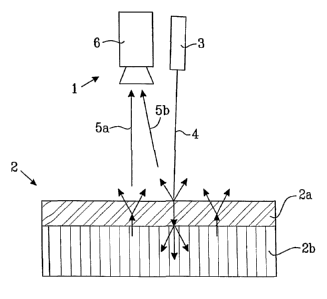
[0027] Figure 1 is a conceptual diagram showing a basic constitution of a
measuring
system 1 for imaging the characteristics of an object 2 having at least a
first 2a and a
second 2b layer according to a first embodiment of the present invention. The
system 1
comprises at least one light source 3 arranged to illuminate the object 2 with
incident
light 4. An imaging sensor 6 is arranged to detect reflected light 5a and 5b
from the
object 2 and to convert the detected light into electrical charges. Reflected
light which is
detected by the imaging sensor 6 is denoted 5b and, light scattered in the
object which is
detected by the imaging sensor 6 is denoted 5a. The system further comprises
means for
creating an analogue or digital representation of the object 2 according to
the electrical
charges, such as an image/signal-processing unit (not shown). Said means for
creating
the analogue or digital representation of the object 2, may either be a
separate unit or
integrated in the imaging sensor 6. In the preferred embodiment of the present
invention, a digital representation of the object 2 is created.
[0028] The object 2 and the measuring system 1 are moved in relation to one
another in
a predefined direction of movement on parallel planes, preferably in a
substantially
CA 02539269 2006-03-16
WO 2005/031326 PCT/SE2004/001375
horizontal direction. In the preferred embodiment of the present invention the
object 2
moves relative to the measuring system 1. The object 2 may e.g. be placed on a
conveyor belt which moves or alternatively there is no belt and the object
itself moves,
for example, if said object is paper in a continuous web in a paper-making
machine.
5 Instead of the object 2 moving relative to the measuring system 1, the
relationship may
naturally be reversed, that is to say the object 2 is stationary and the
measuring system
1 moves over the object 2 when measuring. In still another embodiment both the
object
2 and the measuring system 1 move in relation to each other.
[0029] The incident fight has limited dispersion in at Least one direction.
Thus, the light
source 3 generate, for example, point light, linear light or light composed of
multiple,
substantially point or linear segments and may be of any type suitable to the
application,
for example a laser, a light-emitting diode (LED), ordinary light (tight
bulb), which are
familiar to the person skilled in the art and will not be further described
herein.
[0030] The light source 3 comprises in one embodiment of the present invention
a
polarizer (not shown), which polarises the incident light 4. This facilitates
in making a
distinction between reflected and scattered light, since the reflected light
also will be
polarized but the scattered light will be polarised to a Lesser degree. When
the fight
source 3 comprises a potarizer, it is necessary to use a sensor that
distinguish between
light polarized in different directions.
[0031] The imaging sensor 6 may be a CCD camera, a CMOS camera, or any other
sensor suitable for imaging characteristics of an object.
[0032] The system further comprises means for obtaining information on light
scattered
in the first layer Za and/or the second layer 2b of the object 2 from the
digital
representation. This read out information is compared with stored information,
such as a
threshold value, in order to detect defects on or in the object 2, e.g. the
light intensity in
each point of the digital representation may be compared to a predetermined
value. The
type of defect can in this manner be classified. Other well-known
classification methods
are of course possible to use, such as comparing the relative light intensity
between two
adjacent points of the digital representation with a predetermined value, etc.
[0033] The object 2 may for example be a laminated product comprising two or
more
different materials or, comprising two or more layers of the same material
assembled
with different directions of the grain of the material. Or, may be a package
wrapped in a
transparent or semi-transparent material, such as a foil, which may be
laminated or
CA 02539269 2006-03-16
WO 2005/031326 PCT/SE2004/001375
6
unlaminated. More examples are food wrapped in or covered by a transparent or
semi-
transparent material, such as a plastic, or an electronic component, such as a
printed
circuit board, covered by a protecting layer. The thickness of the layers may
be equal or
different. The first layer may be only a layer of lacquer. The invention is
not limited to
any specific example of objects. The invention is based on that some materials
scatter
light very well and that the scattered light is affected by the underlying or
overlying
material (layer).
[0034] Some examples of detected and classified defects are listed below and
illustrated
in figures 2a-4b. All of the illustrated examples comprise two layers, but the
invention
works well on objects having more than two layers. Information of the object
to be
inspected is stored, i.e. what the "normal" image on the sensor should look
like (how
light normally is reflected and scattered). Dependi ng on which divergence
from the
"normal" image the captured image has, the type of defect can be classified.
[0035] Figures 2a and 2b illustrates a first example of a defect detected and
classified by
the inventive system, where the first layer 2a transmits light and the second
layer 2b
scatters light. Figure 2a shows incident light 4 which hits the first layer
2a, some of the
incident 4 light is reflected and some of it enters the first layer 2a. The
entered light is
transmitted through the first layer 2a and enters the second layer 2b where it
is
scattered. The scattered light re-enters the first layer 2a, is transmitted
therethrough
and leaves the first layer 2a whereby it is detected by the sensor 6 (shown in
figure 1).
[0036] If, however, the second layer 2b has a defect, there will be a
reduction of the
scattered light detected by the imaging sensor. In this simplified example,
shown in
figure 2b, the sensor will only detect reflected light.
[0037] Figures 3a and 3b illustrates a second example of a defect detected and
classified
by the inventive system, where both the first layer 2a and the second layer 2b
transmit
light. Incident light 4 hits the first layer 2a some of which is reflected and
some of which
enters the first layer 2a. The entered light is transmitted through the first
layer 2a and
enters the second layer 2b, through which it is also transmitted.
[0038] If, however, the object 2 is delaminated, i.e. there is a space between
the first 2a
and the second 2b layer, there will be an increase of scattered light detected
by the
imaging sensor, shown in figure 3b. This is due to the reflection of the light
on the
second layer 2b leading to increased scattered light.
CA 02539269 2006-03-16
WO 2005/031326 PCT/SE2004/001375
[0039] Figures 4a and 4b illustrates a third example of a defect detected and
classified
by the inventive system, where the first layer 2a scatters light and the
second layer 2b
transmits light. Incident light 4 hits the first layer 2a some of which is
reflected and some
of which enters the first layer 2a. The entered light is partly transmitted
through the first
layer 2a and partly scattered therein. The scattered light leaves the first
layer 2a and is
detected by the imaging sensor. The transmitted light enters the second layer
2b and is
transmitted therethrough.
[0040] If, however, there is a defect on the first layer 2a such as a missing
piece, there
will be a reduction of scattered light detected by the imaging sensor. In the
example
shown in figure 4b, only reflected light on the second layer 2b is detected by
the imaging
sensor.
[0041] Another example (not shown) of a defect detected and classified by the
inventive
system, is where the first layer scatters light and the second layer 2b
reflects light. If
there is a defect on the second layer, such as a missing piece, a reduction of
the
scattered light will be detected by the imaging sensor.
[0042] Figure 5a illustrates the measuring system~according to the first
embodiment of
the present invention corresponding to figure 1. The system 1 comprises at
least one
light source 3 arranged to illuminate the object 2 with incident light 4. An
imaging sensor
6 is arranged to detect reflected light from the object 2. In this embodiment
the light
source 3 has generated a line of light 7 across the object 2. The object 2
comprises a
defect 8 which in figure 5a is located within the field of view (FoV) of the
imaging sensor
6.
[0043] The image of the object in figure 5a captured on the two-dimensional
sensor 6 is
shown in figure 5b. The sensor detects both the light scattered in the regions
B1 and B2
in the object 2 and the reflected light A on the object 2. Figure 5b shows the
line of light
7 (shown in figure 5a) as A. On both sides of the reflected light A an area of
scattered
light appears which can be seen in figure 5b.
[0044] If the light source 3 comprises a polarizer, the regions B1 and B2 may
be moved
closer to the line of light A on the object 2 without cross-talk between the
reflected and
scattered measurements. This enables detection of small defects.
CA 02539269 2006-03-16
WO 2005/031326 PCT/SE2004/001375
?j
[0045] The intensities (signal strengths) of the reflected Light A and the
scattered light B
in the captured image in figure 5b are shown in figure 5c. The indicated
defect 8 which
yields an increased scatter is clearly visible in figure 5c.
[0046] If the complete image is retrieved from the sensor, the processing to
find the
intensity of the scattered and reflected light is made by an external signal-
processing
unit. The output of raw sensor information limits, however, the possible
sampling speed.
If the sensor has random access capability it is possible to extract only the
interesting
regions from the sensor, thus retrieving a smaller amount of data from the
sensor and a
possibility to reach a greater sampling speed. With some sensors it is also
possible to
have different exposure time and/or read-out amplification for the two regions
and also
to sum the scattered light from a number of rows to further increase the
signal strength.
[0047] The scattered light may be collected on one side, B1 or B2, of the
reflected light
or summed up from both sides, B1 and B2, to further increase the signal
strength. If a
point light source is used, a multitude of positions may be used together or
independent
of each other to determine the amount of scattered light. Thus, information on
the main
direction of the scattered light may be obtained.
[0048] Figure 6 shows a setup of the inventive measuring system according to a
second
embodiment of the present invention. In this embodiment, the system 1
comprises one
light source 3 arranged to illuminate the object 2 with incident light 4. An
imaging sensor
6 is arranged to detect reflected light 5a and 5b from the object 4 and to
convert the
detected light into electrical charges. Reflected light which is detected by
the imaging
sensor 6 is denoted 5b and, light scattered in the object which is detected by
the imaging
sensor 6 is denoted 5a. The system further comprises means for creating an
analogue or
digital representation of the object 2 according to the electrical charges,
such as ~an
image/signal-processing unit (not shown). In the preferred embodiment a
digital
representation is created. Said means for creating the digital representation
of the object
2, may either be a separate unit or integrated in the imaging sensor 6. In
this setup of
the measuring system 1, the light source 3 is placed at a distance away from
the imaging
sensor 6 in order to besides obtaining information o n scattered light also
obtaining
information on the geometric profile of at least one of tile layers 2a or 2b
of the object 2
from the digital representation.
[0049] The information on the geometric profile of the object 2, i.e. the
object shape
information, is obtained by using triangulation, i.e. the position of the
reflected light
indicates the distance from the sensor 6 to the object 2.
CA 02539269 2006-03-16
WO 2005/031326 PCT/SE2004/001375
9
[0050] The setups in figures 1 and 6 comprise a single light source 3. It is,
however
obvious for the person skilled in the art that more than one light source can
be used. For
example, in the second embodiment of the present invention shown in figure 6,
different
light sources may be used for the three-dimensional (geometry) and the two-
dimensional
(scattered light) images. This can even increase the imaging speed in some
cases.
[0051] Figure 7a illustrates the measuring system according to the second
embodiment
of the present invention corresponding figure 6. The system 1 comprises at
least one
light source 3 arranged to illuminate the object 2 with incident light 4. An
imaging sensor
6 is arranged to detect reflected light 5 from the object 2. In this
embodiment the light
source 3 has generated a line of light 7 across the object 2. The object 2
comprises a
defect 8 which in the figure 7a is located within the field of view (FoV) of
the imaging
sensor 6.
[0052] The image of the object in figure 7a captured on the two-dimensional
sensor 6 is
shown in figure 7b. Figure 7b shows the line of light 7 (shown in figure 7a)
as A. On both
sides of the reflected light A an area of scattered light appears which can be
seen in
figure 7b. The sensor detects both the light scattered in the regions B1 and
B2 in the
object 2 and the reflected light in A on the object ~. The shape (geometry) of
the object
2 is shown with the bold line A in figure 7b. The geometry of the object
(indicated with C
in figure 7c) follows line A, i.e. the reflected light. The regions B1 and B2
are in parallel
with line A.
[0053] The intensities (signal strengths) of the reflected light A and the
scattered light B
in the captured image in figure 7b are shown in fig ure 7c. The indicated
defect 8 which
yields an increased scatter is clearly visible in figure 7c. Figure 7c further
shows the
range profile C extracted from the shape of A shown in 7b.
[0054] In the following will be described a method for imaging the
characteristics of an
object having at least a first and a second layer by means of a measuring
system, in
which method the object is illuminated by means of incident light, and light
reflected
from the object is detected by means of an imaging sensor in which the
detected light is
converted into electrical charges, according to which a representation of the
object is
created, wherein information on light scattered in the first layer and the
second layer of
the object' is obtained from the representation and that the information is
compared to
stored information in order to detect defects on the object.
CA 02539269 2006-03-16
WO 2005/031326 PCT/SE2004/001375
[0055] In a further embodiment of the method the measuring system and/or the
object
is/are moved in relation to one another in a predefined direction of movement.
[0056] In another embodiment the method further comprises the step of
obtaining
5 information on the geometric profile of the object from the representation,
either the first
layer of the object or the second layer of the object.
[0057] In still another embodiment the method further comprising the step of
using
polarized incident light in order to facilitate the distinction between
reflected light on the
10 object and scattered light in the object.
[0058] As illustrated by the above, a measuring system and a method for
imaging the
characteristics of an object having at least a fi rst and a second layer by
means of the
measuring system has been described, where defects may be detected in both the
first
and the second layer. The approach according to the present invention being
advantageous in comparison to the previously discussed prior art approach,
which
detects defects in only a wrapping layer of an object The present invention
eliminates
these restrictions of such a prior art approach through enabling the detection
of defects
in either one of the first and the second layer of the object or both.
[0059] Thus, while there have been shown and described and pointed out
fundamental
novel features of the invention as applied to a preferred embodiment thereof,
it will be
understood that various omissions and substitutions and changes in the form
and details
of the devices illustrated, and in their operation, may be made by those
skilled in the art
without departing from the spirit of the invention. For example, it is
expressly intended
that all combinations of those elements and/or method steps which perform
substantially
the same function in substantially the same way to achieve the same results
are within
the scope of the invention. Moreover, it should be recognized that structures
and/or
elements and/or method steps shown and/or described in connection with any
disclosed
form or embodiment of the invention may be incorporated in any other disclosed
or
described or suggested form or embodiment as a general matter of design
choice. It is
the intention, therefore, to be limited only as indicated by the scope of the
claims
appended hereto.