Note: Descriptions are shown in the official language in which they were submitted.
CA 02539539 2006-03-20
WO 2005/030376 PCT/US2004/031283
STRESSED THIN-FILM MEMBRANE ISLANDS
Related Application
This application claims the benefit of U.S. Provisional Application 60/505,547
filed
September 23, 2003, the entire disclosure of which is hereby incorporated by
reference.
Field of the Invention
The invention relates generally to stressed membranes and specifically to
stressed thin-
film membranes for which fluidic access is required to both sides of the
membrane.
Back r
Many commercial applications require the separation of two fluids, e.g.,
gasses or liquids,
by using a membrane. The membrane is selected to mediate the interaction of
the two fluids.
For example, in a hydrogen purification system, the membrane may mediate the
interaction of a
hydrogen-rich stream at high pressure from a pure hydrogen stream at lower
pressure. In this
example, the membrane may be constructed from a material that allows hydrogen
diffusion at a
higher rate than other components of the hydrogen-rich stream. In another
example, a membrane
in a fuel cell may mediate the interaction of an oxygen-containing fluid with
a fuel-containing
fluid. The fuel cell membrane may include multiple layers that allow one or
more types of ions
to pass through the membrane to oxidize the fuel, while extracting electrical
energy from that
reaction.
To improve performa~ice and decrease system size, it is often desirable to
miniaturize
membrane-containing systems. However, the materials that can readily be
manufactured in a
miniaturized fashion are not always compatible with the materials that are
optimal for membrane
functionality. Integration of these two materials sets may result in
substantial stresses in the
membrane. Stress may be induced by, for example, different thermal expansion
rates of the
membrane and a supporting structure.
A specific example of a need for miniaturization may be found in the area of
batteries
and fuel cells. The proliferation of portable electronics, including cellular
telephones and laptop
computers, has increased the demand on power storage devices, such as
batteries. Fuel cells may
be used to increase energy storage available in comparison to batteries. The
fuel cell system,
however, must be miniaturized to fit within the small form-factors of existing
batteries. One
CA 02539539 2006-03-20
WO 2005/030376 PCT/US2004/031283
-2-
example of a type of fuel cell is a solid oxide fuel cell, which is known to
have high efficiency.
One common miniaturization tecluuque employs silicon (Si) substrates and
integrated circuit
manufacturing technologies. Silicon expands at a rate of approximately 4
micrometers per meter
per degree Celsius (~,mhn/°C). Conventional solid oxide fuel cells use
materials that expand at a
rate of approximately 10 ~,mlm/°C, and operate at temperatures of about
800 °C. Combining a
conventional solid oxide fuel cell membrane with conventional silicon
manufacturing may cause
a significant expansion mismatch of approximately 0.5%, leading to highly
stressed membranes.
Additional factors contributing to the stress may include intrinsic stress of
the thin film as
deposited, tensile or compressive stress induced by sintering or other thermal
processing, and
chemical modifications inducing tensile or compressive stresses. High stresses
in the thin-film
membranes may cause mechanical failure of the film or the stress level may
undesirably change
material properties.
Design of fuel cell membranes, such as yttrium-stabilized zirconia (YSZ) on Si
substrates, may require a free-standing YSZ thin film to stretch over a 1
millimeter (mm) to a 1
centimeter (cm) diameter. These membranes may fail because these membranes may
be pliable
or prone to budding. Furthermore, YSZ membranes may also fail when cooled into
the tensile
state because of crack propagation.
Summary
The invention relates to the formation of stressed thin-film membranes
substantially free
of craclcs, configured so that fluidic contact to both sides of the membranes
is possible.
In the particular case of a tensilely stressed film fully bonded to a rigid
support, channel
fractures or cracks in a web-like pattern may form in the film. A distance
between adjacent
craclcs is observed not to be random, but rather to cluster near a
characteristic crack spacing.
This phenomenon is well known in the field of thin film fracture mechanics.
Reducing lateral dimensions of the tensilely stressed film below this
characteristic crack
spacing helps prevent the film from cracking. In order to produce larger
active areas of stressed
material, arrays of islands of stressed films may be formed.
The existing techniques of island formation cannot be readily adapted for the
formation
of tensilely stressed membranes, i.e., membrane structures that allow fluidic
access to both sides
of a film. The requirement for fluidic contact means that stressed membranes
cannot be disposed
over solid support structures.
CA 02539539 2006-03-20
WO 2005/030376 PCT/US2004/031283
-3-
In the particular case of a compressively stressed membrane, the laclc of a
supporting
structure may result in expansion and warping of the membrane. This waxping
may be
undesirable for various applications, and may also cause cracking of the
membrane.
Providing good adhesion to the substrate such that the bonding energy is
larger than the
energy in the stressed material may help prevent compressive failure. However,
this existing
technique of improved adhesion cannot be readily adapted for the formation of
stressed
membranes.
A structure in accordance with the invention is a small tensilely stressed
membrane that
has only a slight overlap with a supporting structure, i.e., a support grid.
The total dimensions of
the stressed material, including freestanding and bonded areas, are designed
to be sufficiently
small so that the membrane is unlikely to fracture in tension. The allowable
dimensions for a
tensilely stressed membrane are dictated by the characteristic crack spacing.
Materials at the
bond interface, i.e., the support grid, affect the characteristic crack
spacing, and therefore also
affect the allowed dimensions of the membrane.
In an embodiment, the available active area is increased by the construction
of islands
axranged such that the spacing between islands is relatively small. This
embodiment may be
referred to as "pre-cracking" of the film because of the similarities between
the intentional
spacings and the cracks that would have formed if not for the creation of the
spacings. The
support structure may be a support grid aligned under the spaces with a small
overlap with the
stressed film. The dimensions of the support structure are designed according
to design rules
presented below so that the film is unlikely to craclc in tension.
Another structure in accordance with the invention is a small compressively
stressed
membrane that is bonded to the support material. The allowable dimensions of
the free-standing
area of the film are designed according to design rules presented below so
that the membrane is
unlikely to buclcle in compression.
In one embodiment, a support grid is provided to which the membrane may be
bonded,
and a method is provided for forming an appropriate seal around an outer edge
of the membrane.
The support grid, including a material such as silicon-rich silicon nitride,
helps provide stiffness
to the membrane structure, as well as reduces the probability of warping. A
small island of
stressed thin-film material is rigidly bonded to a support material over an
annulus near an outer
edge of the island. Additional areas located throughout the film may also be
bonded.
In an embodiment, the available active area is increased by the construction
of
compressively stressed membranes arranged such that the spacing between
membranes is
CA 02539539 2006-03-20
WO 2005/030376 PCT/US2004/031283
-4-
relatively small. Adjacent membranes may be formed from a continuous section
of thin-film
material. The dimensions of the support structure are designed according to
design rules
presented below so that the support structure is unlikely to buckle in
compression.
A third structure in accordance with the invention combines the features of
the above two
structures to accommodate membranes which may be under tensile and compressive
stress at
various operating conditions, times, or locations. This structure is a small
stressed membrane
that has only a slight overlap with the supporting structure, i.e., a support
grid. The total
dimensions of the stressed material, including freestanding and bonded areas,
are designed to be
sufficiently small so that the membrane is unlikely to fracture in tension
according to the tensile
design rules presented below. The allowable dimensions for the support opening
are based on
the dimensions calculated using the compressive design rules presented below.
Materials at the
bond interface, i.e., the support grid, affect the characteristic crack
spacing, and therefore also
affect the allowed dimensions of the membrane.
The membranes of the invention may be designed to survive repeated thermal
cycling.
These membranes may be, for example, micro-electro-mechanical system (MEMS)
based solid-
oxide fuel cell membranes.
In am aspect, the invention features a structure including a support defining
a first
opening, and a first tensilely stressed thin-film membrane disposed to occlude
the first opening,
the first stressed thin-film membrane contacting at least a first portion of
the support. The first
tensilely stressed thin-film membrane includes a membrane material having a
characteristic
crack spacing greater than one-half of a minimum dimension of the first
stressed thin-film
membrane and less than ten times the minimum dimension.
One or more of the following features may be included. The support may define
a
second opening adjacent to the first opening, the structure also including a
second tensilely
stressed thin-film membrane disposed to occlude the second opening, the second
stressed thin-
film membrane contacting at least a second portion of the support. The second
tensilely stressed
thin-film membrane may include the membrane material and the characteristic
crack spacing is
greater than one-half of a minimum dimension of the second stressed thin-film
membrane and
less than ten times the minimum dimension of the second tensilely stressed
thin-film membrane.
A distance between the first and second openings may be less than the minimum
dimension of
each opening.
The membrane may be disposed in an array and the array may include a plurality
of
stressed thin-film membranes and openings. A shape of the opening may be
hexagonal, square,
CA 02539539 2006-03-20
WO 2005/030376 PCT/US2004/031283
-5-
triangular, or circular. A cross-sectional portion of the support may define a
first shelf and an
extension, and the stressed thin-film membrane may contact a portion of the
first shelf. The
cross-sectional portion of the support may define a second shelf disposed in
parallel to the first
shelf, and the stressed thin-film membrane may contact a portion of the second
shelf. The
characteristic craclc spacing may be less than 1 mm. The stressed thin-film
membrane may be
disposed in an electrochemical system, e.g., a solid oxide fuel cell, or in a
membrane-based
hydrogen separation system.
The stressed thin-film membrane may include a material such as copper, nickel,
palladium, platinum, rhenium, silicon carbide, aluminum nitride, an oxide,
and/or combinations
thereof. The oxide may be, e.g., an oxide of aluminum, cerium, chromium,
cobalt, hafnium,
iron, la~lthanum, magnesium, manganese, samarium, scandium, silicon,
strontium, titanium,
ytterbium, yttrium, zirconium, praseodymium, and/or combinations thereof.
In another aspect, the invention features a structure including a support
defining a first
opening having a minimum opening dimension, and a first compressively stressed
thin-film
membrane disposed to occlude the first opening, the first stressed thin-film
membrane contacting
at least a first portion of the support. The first compressively stressed thin-
film membrane
includes a membrane material, a critical aspect ratio for buclcling of the
membrane material is
greater than a ratio of one-half of the minimum dimension of the first opening
to a thiclcness of
the stressed thin-film membrane, and the critical aspect ratio for buckling is
less than a ratio of
ten times the minimum dimension of the first opening to the thickness of the
stressed thin-film
membrane.
One or more of the following features may be included. The support may define
a
second opening adjacent to the first opening, and a secoild compressively
stressed thin-film
membrane may be disposed to occlude the second opening, the second stressed
thin-film
membrane contacting at least a second portion of the support. The second
compressively
stressed thin-film membrane may include the membrane material, a critical
aspect ratio for
buclcling of the membrane material may be greater than a ratio of one-half of
a minimum
dimension of the second opening to a thiclcness of the stressed thin-film
membrane, the critical
aspect ratio for buckling may be less than a ratio of ten times the minimum
dimension of the first
opening to the tluckness of the stressed thin-film membrane, and the critical
aspect ratio for
buckling may be less than a ratio of ten times the minimum dimension of the
second opening to
the thickness of the stressed thin-film membrane.
CA 02539539 2006-03-20
WO 2005/030376 PCT/US2004/031283
-6-
A distance between the first and second openings may be less than the minimum
dimension of each opening.
The membrane may be disposed in an array, the array including a plurality of
first
stressed thin-film membranes and openings, and a critical aspect ratio for
buckling of the array is
less than the ratio of a minimum dimension of the array to the effective array
thickness. The
critical aspect ratio for buckling of the membrane material may be less than
40:1. The shape of
the opening may be, e.g., hexagonal, square, triangular, or circular. A cross-
sectional portion of
the support may define a first shelf and an extension, and the stressed thin-
film membrane may
contact a portion of the first shelf. The cross-sectional portion of the
support may def se a
second shelf disposed in parallel to the first shelf, and the stressed thin-
film membrane may
contact a portion of the second shelf.
The characteristic crack spacing may be less than 1 mm. The stressed thin-film
membrane may be disposed in an electrochemical system, e.g., a solid oxide
fuel cell or a
membrane-based hydrogen separation system.
The stressed thin-film membrane may include a material such as copper, nickel,
palladium, platinum, rhenium, silicon carbide, aluminum stride, an oxide,
and/or combinations
thereof. The oxide may be, e.g., an oxide of aluminum, cerium, chromium,
cobalt, hafnium,
iron, lanthanum, magnesium, manganese, samarium, scandium, silicon, strontium,
titanium,
ytterbium, yttrium, zirconium, praseodymium, and combinations thereof.
In another aspect, the invention features a structure including a support
defining a first
opening, and a first stressed thin-film membrane comprising a membrane
material disposed to
occlude the first opening, the first stressed thin-film membrane contacting at
least a, first portion
of the support. At a first operating condition, the first stressed thin-film
membrane is tensilely
stressed and the membrane material has a characteristic crack spacing greater
than one-half of a
minimum dimension of the first stressed thin-film membrane and less than ten
times the
minimum dimension. At a second operating condition, the first stressed thin-
film membrane is
compressively stressed and a critical aspect ratio for buckling of the
membrane material is
greater than a ratio of one-half of a minimum dimension of the first opening
to a thickness of the
stressed thin-film membrane, and the critical aspect ratio for buckling is
less than a ratio of ten
times the minimum dimension of the first opening to the thickness of the
stressed thin-film
membrane.
CA 02539539 2006-03-20
WO 2005/030376 PCT/US2004/031283
_ '7 _
In another aspect, the invention features a method of forming the structures
described
above, including the steps of forming a support defining an opening, and
forming a stressed thin-
film membrane to occlude the opening.
One or more of the following features may be included. A substrate may be
provided, forming
the support includes forming the support in at least a region of a substrate,
and the stressed thin-
film membrane contacts both the support and the substrate. At least a portion
of the substrate
may be removed. An additional material may be deposited onto the stressed thin-
film
membrane.
Forming the support may include forming a sacrificial layer over the
substrate, defining a
cavity in the substrate and the sacrificial layer, at least partially filling
the cavity with a support
material, and removing at least a portion of the sacrificial layer to expose
at least a portion of a
top surface of the support material.
The foregoing, and other features and advantages of the invention, as well as
the
invention itself, will be more fully understood from the description and
drawings that follow.
Brief Description of Drawings
Figures 1 - 11 G are schematic cross-sectional and top views of the
fabrication of an
embodiment of the invention and schematic top views of masks used therein;
Figure 12 is a schematic cross-sectional view of an embodiment of the
invention;
Figures 13a - 13b are a schematic view of an embodiment of the invention in
use with an
electrochemical system and a solid oxide fuel cell; and
Figure 14 is a schematic view of an embodiment of the invention in use with a
hydrogen
separation system.
The drawings are not necessarily to scale, emphasis instead generally being
placed upon
illustrating the principles of the invention. The advantages of the invention
can be better
understood by reference to the description talcen in conjunction with the
accompanying
drawings.
Detailed Description
A stressed thin-film structure may be formed in accordance with the following
process
flow. Referring to Figure 1, a substrate 10 may include a semiconductor
material, such as
double-sided polished silicon, and may have a diameter of, e.g., about 100 mms
(mm) (not
shown) and a thickness to of, e.g., about 50 - 500 ~,m. A sacrificial layer 20
is formed over the
CA 02539539 2006-03-20
WO 2005/030376 PCT/US2004/031283
_g_
substrate 10. The sacrificial layer may include a dielectric material, such as
silicon dioxide
(Si02). In an embodiment, the sacrificial layer 20 may be grown on both a
front side 12 and a
backside 14 of substrate 10 by, e.g., steam oxidation. Steam oxidation may be
performed in, for
example, in a furnace system available from Tystar Corporation, based in
Torrance, CA, in a
steam ambient at 1050 °C. The sacrificial layer 20 may have a thiclmess
t1 sufficiently thick to
enable the subsequent formation of ribs 120 (see, e.g., Figure 8) having a
height at least equal to
a thickness of the subsequently formed stressed thin-film membrane 190 (see,
e.g., Figure 11A).
Thiclcness t1 of the sacrificial layer may be, for example, approximately 2
~.m.
Referring to Figures 2A - 2D, a grid pattern 30 is defined in sacrificial
layer 20 and
substrate 10 by, e.g., photolithography and etching. A photoresist layer 40 is
spun on, exposed,
and developed over the sacrificial layer 20. The photoresist layer has a
thickness t2 that is
sufficiently thick to withstand further processing, e.g., t2 may be about 2
~.m. The grid pattern
30, as initially defined by patterning the photoresist layer 40, may include
an opening 45 having
a width w1 of, e.g., about 1.5 ~,m. The width w1 of the opening 45 is selected
such that the
subsequently defined support grid structure 90 (see, e.g., Figure 11A) will
provide sufficient
rigidity without drastically reducing the active area of membranes 190 (see,
e.g., Figure 1 1A).
The grid pattern 30 is defined by using a grid mask 46 to pattern the
photoresist layer 40.
The grid mask 46 includes a mask grid pattern 47 defining a plurality of cells
48. The mask grid
pattern may have length to of, e.g., about 750 ~m and a height ho of, e.g.,
about 750 ~,m. Each
cell may have a geometric shape, i.e., a hexagon with a distance do between
parallel sides of,
e.g., 10 to 40 ~.m, in accordance with the design rules presented below. A
plurality of cells may
form a honeycomb pattern, as defined by the maslc grid pattern. The grid mask
may define a die
having a height hl and a length 11 of, e.g., about 10 mm each.
Referring also to Figure 3, after the photoresist layer 40 is defined,
portions 50 of the
sacrificial layer 20 exposed by openings 45 in the photoresist layer 40 are
removed by, for
example, dry etching. Dry etching may be performed by, for example, reactive
ion etching (RIE)
in an etclung system such as the AMT 8100 system, manufactured by Applied
Materials, Santa
Clara, CA, with an etching recipe appropriate fox the composition of the
sacrificial layer, e.g., an
oxide etch recipe. This etch may be an anisotropic etch that defines a
plurality of openings 60 in
the sacrificial layer 20 having a width wa that is approximately equal to w1,
e.g., about 1.5 ~,m.
Referring to Figure 4, after etching through sacrificial layer 20, an
isotropic etch is
performed, extending into substrate 10 to form a plurality of depressions 70.
In an embodiment
in which the substrate is formed of Si, this isotropic etch may be an sulfur
hexafluoride (SF6)
CA 02539539 2006-03-20
WO 2005/030376 PCT/US2004/031283
_g_
etch performed for about 60 - 300 seconds by, e.g., a Multiplex system,
manufactured by Surface
Technology Systems, Wales, United Kingdom. This etch step defines depressions
70 in a
substrate, where the depressions have a depth dl of, e.g., about 3 - 4 ~,m and
a width ws of about
8 ~,m. Depth dl and width w3 are selected such that the support grid 90,
subsequently formed in
part in depressions 70 (see Figure 1 1A), provides adequate support for
subsequently formed
stressed thin-film membranes 190 (see Figure 11A) without excessively reducing
an active area
of these membranes 190.
Referring to Figure 5, the isotropic etch into substrate 10 is followed by an
anisotropic
etch to define a plurality of extensions 80 of the depressions 70. Extensions
80 may be trenches
defined in the substrate. The extensions may be formed by, e.g., an ausotropic
etch in a system
such as the Multiplex system. In an embodiment in which the substrate 10
contains silicon, an
appropriate etch may be a recipe that uses an SF6 and octafluorocyclobutane
(C4F8) chemistry.
A method for anisotropically etching silicon is described in, for example,
U.S. Patent No.
5,501,893. Extensions 80 may each have a depth d2 of, e.g., about 30 - 40 Vim.
The depth d2 of
extensions 80 is selected such that the material subsequently deposited in
extensions 80 (see
below) provides sufficient support, using the design rules for compressively
stressed thin-film
membranes presented below, to the subsequently formed stressed thin-film
membrane, but
sufficiently shallow such that gas flow to the membrane is not hindered. For
some embodiments
with tensilely stressed thin-film membranes, the extension may not be needed.
After these etch
steps, the photoresist layer 40 is stripped. The substrate 10 may then be
cleaned by, e.g., an
RCA clean followed by, e.g., a one-hour oxidation step at 800 °C to
eliminate any residual
polymer. The grid pattern 30, initially defined by photoresist 40, is now
defined by openings 60,
depressions 70, and extensions 80.
Referring to Figure 6, a support grid 90 is defined by deposition of a support
material 100
that may be, for example, a dielectric such as silicon-rich silicon nitride or
Ti02, over sacrificial
layer 20 and into grid pattern 30, including openings 60, depressions 70, and
extensions 80. The
support material 100 may be deposited by, for example, chemical vapor
deposition (CVD), e.g.,
low-pressure CVD (LPCVD) or plasma-enhanced CVD (PECVD). The support material
100
may be under low stress, e.g., <300 MPa, and may have a thickness t3 of, e.g.,
about 2 p,m. The '°
compressive stress of the support material 100 should be sufficiently low to
prevent bucl~ling
according to the compressive design rules presented below. The tensile stress
is limited by the
tensile strength of the support material 100. The support grid 90 may be
formed from a
CA 02539539 2006-03-20
WO 2005/030376 PCT/US2004/031283
-10-
dielectric material to prevent electrical shorts in the final structure, e.g.,
in a fuel cell
embodiment.
Referring to Figure 6 and 7, a top portion 105 of support material 100 is
removed by,
e.g., a dry etch, such as a nitride etch in the AMT 8100 system. Visual
clearance endpoint
detection may be used, with an overetch of approximately 5%.
Referring to Figures 7 and 8, removal of the top portion 105 of support
material 100
exposes a portion 110 of sacrificial layer 20. The sacrificial layer may be
selectively removed
by, for example, a wet etch. For example, in an embodiment in which the
sacrificial layer
includes oxide, it may be removed by an oxide etch such as a buffered oxide
etch (BOE) that
includes hydrofluoric acid, ammonia fluoride, and water. The removal of the
sacrificial layer
may be followed by a cleaning step such as an SC-1 (NH40H:H202) cleaning step,
or an RCA
clean followed by a one hour wet oxidation at 800 °C. Removal of the
sacrificial layer 20
exposes a portion of the support grid 90. This exposed poution includes rib
120 that has been
formed by the deposition of support material 100 into opening 60 in
sacrificial layer 20. The ribs
120 define generally the same pattern that had been originally defined by
maslc 47, e.g., a
plurality of hexagons. The ribs have a height h2 approximately equal to an
initial thiclcness t2 of
the sacrificial layer, e.g., about 2 pm. The exposed portion of support grid
90 forms a shelf 125.
Referring to Figure 9, a stressed thin-film layer 130 is formed over the ribs
120, exposed
portions of front side 12 of substrate 10, and support grid 90, specifically
over depressions 70
filled with support material 100. The stressed thin-film layer may be, e.g.,
deposited, such as by
electron-beam evaporation. The stressed thin-film layer may include a membrane
material that
functions as an electrolyte material, for example, YSZ, ox may include a
membrane material that
functions as an electrode, such as for example, a niclcel/yttrium-stabilized
zirconia composite.
YSZ is a material particularly suitable for use as an electrolyte in a solid-
oxide fuel cell because
it is a material selectively permeable to oxygen ions at various partial
pressures of oxygen. In
summary, some materials that may be used as a membrane material to form the
stressed thin-film
layer include copper, niclcel, palladium, platinum, rhenium, silicon carbide,
aluminum nitride, an
oxide such as an oxide of aluminum, cerium, chromium, cobalt, hafnium, iron,
lanthanum,
magnesium, manganese, samarium, scandium, silicon, strontium, titanium,
ytterbium, yttrium,
zirconium, praseodymium, and/or combinations thereof. The stressed thin-film
layer 130 may
have a thickness t4 of, e.g., about 2 p,m.
Depositing the stressed thin-film layer 130 over the ribs 120 may result in a
formation of
intentional discontinuities 135 in the stressed thin-film layer 130 proximate
the ribs 120. These
CA 02539539 2006-03-20
WO 2005/030376 PCT/US2004/031283
-11-
intentional discontinuities may be defined by controlling the step coverage of
the stressed thin-
film layer over the ribs. More specifically, nonconformal coating by the
stressed thin-film layer
130 leads to the formation of discontinuities. The intentional discontinuities
relieve stress in the
stressed thin-film layer, thereby helping to prevent the formation of
unintentional cracks.
Referring to Figures 1 OA and l OB, a release photoresist pattern 140 is
defined over the
backside 14 of substrate 10. As defined by a release mask 150, the release
photoresist pattern
140 may include a die 160 having a length 12 and height h2 of, e.g.,
approximately 10 mm each.
A center portion of the die may define a square 165 having sides with a length
13 of, e.g., about
1.2 mm. Through use of mask 150, photoresist is patterned over substrate
backside 14 such that
the photoresist 140 defines an open square 170 opposite support grid 90.
After the definition of release photoresist pattern, exposed portions of
support material
100 and sacrificial layer 20 are removed. Both layers 100, 20 may be removed
by, e.g., a dry
etch in an AMT 8100 system from Applied Materials.
Referring to Figure 1 1A and 11B, exposed portions of the substrate 10 are
removed by,
for example, a wet etch. In an embodiment in which the substrate includes
silicon, a suitable wet
etch may be a potassium hydroxide (KOH) etch. This composition selectively
etches silicon
along certain planes, resulting in a frame 200 in a shape of a square-based,
flat-topped pyramid,
i.e., an opening 201 created by this etch will be broader at a bottom portion
202 at the backside
14 of substrate 10 and narrower at a top portion 204 proximate the support
grid 90. For example,
if sides of the opening 170 defined by a release mask 150 have a length 13 of,
e.g., approximately
1.2 nun each, the opening proximate the support grid 90 will have a length 14
of, e.g., about 500
~,m. Frame 200 is formed from a same material as substrate 10, e.g., silicon,
and includes frame
walls 205 having a thickness to of, e.g., about 500 ~,m.
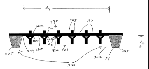
Referring to Figures 11A - 11F, a result of the processing steps described
above is a
compound stressed thin-film membrane structure 175 having a support grid 90
defining a
plurality of openings 180. Each of the openings 180 may have a hexagonal,
square, triangular,
or circular shape. A distance dZO between first and second adjacent openings
180a, 180b may be
less than a minimum dimension d3o of each opening.
The stressed thin-film layer 130 defines a plurality of stressed thin-film
membranes 190,
e.g., electrolyte layers, disposed to occlude the openings 180. The plurality
of stressed thin-film
membranes 190 may include at least a first tensilely stressed thin-film
membrane 190a and a
second tensilely stressed thin-film membrane 190b, disposed to occlude a first
opening 180a and
a second opening 180b, respectively. Alternatively, the plurality of stressed
thin-film
CA 02539539 2006-03-20
WO 2005/030376 PCT/US2004/031283
-12-
membranes 190 may include at least a first compressively stressed thin-film
membrane 190a and
a second compressively stressed thin-film membrane 190b, disposed to occlude a
first opening
180a and a second opening 180b, respectively. The stressed thin-film membranes
(also referred
to as "tiles") each contact at least a portion of the support grid 90. The
first tensilely or
compressively stressed thin-film membrane may contact at least a first portion
195a of the
support and the second tensilely or compressively stressed thin-film membrane
may contact at
least a second portion 195b of the support. The portion of the support grid 90
contacted by the
stressed thin-film membrane may be at least a portion of shelf 125.
The critical craclc spacing and the critical aspect ratio for buckling are the
geometric
values at which the probability of failure through cracking or buckling is
approximately equal to
the probability of not craclcing or buckling. In many practical applications,
it is desirable to have
a very high probability of not failing. In these cases it may be beneficial to
add a factor of safety
to the geometry. For example, the critical crack spacing may be up to two
times the minimum
dimension of the stressed thin-film membrane. Alternatively, the critical
crack spacing may be
up to ten times the minimum dimension of the stressed thin-film membrane. In
the case of
compressive films, the critical aspect ratio for buckling may be up to two
times the ratio of the
minimum opening dimension to the thickness of the stressed thin-film membrane.
Alternatively,
the critical aspect ratio for buclcling may be up to ten times the ratio of
the minimum opening
dimension to the thickness of the stressed thin-film membrane.
These considerations may be taken into account in determining membrane
materials and
geometries. In some embodiments, each tensilely stressed thin-film membrane
includes a
membrane material having a characteristic crack spacing that is greater than
one-half of a
minimum dimension of the membrane and less than ten times the minimum
dimension. This
relationship may also be expressed as follows: the minimum dimension of the
membrane is
between twice and one-tenth the characteristic crack spacing. The membrane
minimum
dimension is determined by a minimum distance between two sides of a shape
defined by the
membrane. For example, each stressed thin-film membrane may have the shape of
a hexagon,
having a minimum dimension equal to a distance do between parallel sides of,
e.g., about 20 ~,m,
as defined by the cells 48 of grid mask 46 (see Figure 2B and 2C). Further
discussion of
characteristic crack spacing is provided below in the discussion of the design
rules.
The maximum dimension of the membrane may also be less than the critical
buclcling
length. A compressively stressed thin-film membrane may include a membrane
material having
a critical aspect ratio for buckling that is greater than a ratio of one-half
of a minimum dimension
CA 02539539 2006-03-20
WO 2005/030376 PCT/US2004/031283
-13-
of the first opening to a thickness of the stressed thin-film membrane, and
the critical aspect ratio
for buclding is less than a ratio of ten times the minimum dimension of the
first opening to the
thiclaiess of the stressed thin-film membrane. This relationship may also be
expressed as
follows: a ratio of the minimum opening dimension to the thickness of the
stressed-thin film
membrane may be between twice and one-tenth of the critical aspect ratio for
buclding.
Further discussion of design rules for preventing bucl~ling is provided below
under the
section heading "~ve~view of Design Rules fog Compressive Stress. "
In some embodiments, the stressed thin-film membrane may be tensilely stressed
at a
first operating condition and the membrane material may have a characteristic
crack spacing
greater than one-half of a minimum dimension of the first stressed thin-film
membrane. At a
second operating condition, the first stressed thin-film membrane may be
compressively stressed
and a critical aspect ratio for buckling of the membrane material may be more
than one-half of a
minimum dimension of the first opening.
Referring to Figures 11B and 11G, compound stressed thin-film membrane
structure 175
may be formed repeatedly across substrate 10, thereby creating a stressed thin-
film membrane
array consisting of two nested and repeating lattice structures, i.e., a
smaller lattice compound
stressed thin-film membrane structure 175 including the stressed thin-film
membranes 190
disposed over support grid 90 and a larger lattice structure 220 including
compound stressed
thin-film membranes 175 disposed over frame 200.
The support grid discussed above produces a support having a "t" shape. In an
alternative embodiment, ribs may be omitted from the compound stressed thin-
film membrane
structure by extending the removal of top portion 105 of support material 100
such that the rib is
removed as well. In this embodiment, therefore, the support grid may have a
"T" shape.
It will be apparent to those skilled in the art that the support grid may have
a variety of
cross-sectional shapes. The grid preferably provides a surface for attachment
of the stressed
thin-film membrane. Referring to Figure 12, a cross-sectional portion of the
support grid 90 may
define a first shelf 300 and an extension 310, and the tensilely or
compressively stressed thin-
film membrane 190 may contact a portion 300a of the first shelf. The cross-
sectional portion of
the support may also define a second shelf 320 disposed in parallel to the
first shelf, and the
stressed thin-film membrane may contact a portion 320a of the second shelf. In
some
embodiments, for example those with compressive films, the grid preferably has
sufficient
dimensions to provide rigidity to the membrane according to the compressive
design rules
provided below. It is found that a deeper grid provides more rigidity than a
wider grid. In a
CA 02539539 2006-03-20
WO 2005/030376 PCT/US2004/031283
-14-
preferred embodiment for compressive stressed thin-film membranes, the ratio
of depth to width
of the grid is greater than 10. In some embodiments, for example those with
tensilely stressed
films, the grid may not provide any siguficant rigidity. For example, the grid
may be a flat thin
film which spans from one stressed thin-film membrane to an adjacent stressed
thin-film
membrane. In other embodiments, particularly with compressively-stressed
membranes,
discontinuities in the membranes may not be needed and a single membra~ie may
occlude more
than one opening, e.g., two or more openings may be occluded by a single
membrane.
In some embodiments of the invention, the grid comprises a dielectric. For
example, in a
fuel cell embodiment, the grid may be selected to be non-conductive to prevent
shorting of the
anode and cathode. In some embodiments of the invention, the grid comprises a
diffusion
barrier. For example, in a hydrogen purification embodiment, the grid may be
selected from a
material with a low diffusion coefficient for gasses.
Referring to Figures 13a and 13b, in use, the stressed thin-film membrane 190
may be
disposed in an electrochemical system 400. An electrochemical system includes
at least a first
. 15 electrode 410, a second electrode 420 and an electrolyte 430 arranged so
that passage of current
between electrodes causes a chemical reaction to occur. The electrolyte may be
defined by the
stressed thin-film membrane 190. The interaction of the chemical species with
the electrodes
also causes a voltage to be generated between the electrodes. Electrochemical
systems can be
used, for example, to generate power such as in a fuel cell. In other
applications,
electrochemical systems can be used to sense the presence or concentration of
various chemical
species. The present invention is particularly useful for electrochemical
systems in which the
first and second electrodes 410, 420 are in communication with both the
electrolyte 430 and a
first fluid 440 and second fluid' 450 respectively, and it is desirable to
maintain separation of the
first and second fluid.
The stressed thin-film membrane may be disposed in a solid oxide fuel cell.
Referring to
Figure 13b, the first fluid 440 may be a fuel and the second fluid 450 may be
an oxidant. The
first electrode 410 may be an anode, the second electrode 420 may be a
cathode, and the
electrolyte 430 may be a solid oxide fuel cell electrolyte defined by stressed
thin-film membrane
190.
Referring to Figure 14, alternatively, the stressed thin-film membrane 190 may
be
disposed in a membrane-based hydrogen separation system 500. A membrane-based
hydrogen
separation system may include at least a first fluid 510, the membrane 190,
and a second fluid
520, with the membrane separating the first and second fluids. The first fluid
510 may include
CA 02539539 2006-03-20
WO 2005/030376 PCT/US2004/031283
-15-
hydrogen and at least a first diluent, with a first ratio of a hydrogen
concentration to a first
diluent concentration. The membrane 190 may include a material selected to be
more permeable
to hydrogen than to the first diluent. This selective permeability allows the
second fluid 520 to
have a second ratio of hydrogen to the first diluent that is lugher than the
first ratio. In some
cases of membranes with extremely high selectivity, the second ratio may
approach infiiuty. In
some applications, a second diluent is added to the second fluid to transport
the hydrogen away
from the membrane.
Desigu Pules
In many embodiments, a compound stressed thin-film membrane structure may be
subjected to a range of stresses during operation. For example, if the stress
is caused in part by
thermal expansion mismatch between stressed thin-film membranes and a support
grid or
between a compound stressed thin-film membrane array and frame, the stress
will vary with
temperature. In another embodiment, the stress may vary over time.
A design for a compound stressed thin-film membrane structure is provided,
such that the
structure is stable throughout the potential stress range. Generally, it is
sufficient to design the
structure to be robust at the extremes of the stress range. In embodiments
with thermal
expansion mismatch-based stress, the extremes generally occur at the highest
and lowest
operating temperatures. One object of this invention is to produce a membrane
that is robust in
both compression and tension.
A compound stressed thin-film membrane structure under excessive stress may
fail, e.g.,
warp (i.e., buclcle) or crack. Failure may occur by compression through cracks
that form as a
result of membrane budding, for example, in the case of a YSZ membrane on
silicon, at higher
temperatures. Failure may also occur by formation of tensile cracks. In an
embodiment with a
YSZ stressed thin-film membranes and a silicon frame, failure by warping in
compression at
elevated temperature generally may initially be more lilcely than failure by
cracking in tension.
In this embodiment, however, tension cracking at lower temperatures may become
more likely
after many hours of device operation because of stress relaxation at elevated
temperatures.
The compound stressed thin-film membrane structure has two features that may
increase
the robustness of a stressed thin-film membrane, such as a YSZ membrane, to
tensile and
compressive stress. Embodiments that include at least one of ribs
(alternatively called "rails" or
"ridges") and film discontinuities may act like stress relief joints, thereby
both reducing the
probability that new cracks will form and preventing cracks that may form from
jumping from
CA 02539539 2006-03-20
WO 2005/030376 PCT/US2004/031283
-16-
one stressed thin-film membrane to an adjacent stressed thin-film membrane.
Any crack that
forms, therefore, is isolated to an individual stressed thin-film membrane,
and is prevented from
causing failure of the compound stressed thin-film membrane structure. The
support grid
imparts stiffness to the compound stressed thin-film membrane structure. This
additional
stiffness may, in some embodiments, prevent or reduce warping of stressed thin-
film membranes
and the compound stressed thin-film membrane structures under compressive
stress.
In some embodiments, particularly with compressively stressed thin-film
membranes,
film discontinuities may not be needed to reduce the risk of craclcs. A single
membrane may,
therefore, occlude more than one opening, e.g., two or more openings may be
occluded by a
single membrane.
Truly robust compound stressed thin-film membrane structures may be achieved
by the
application of a set of geometric design rules intended to prevent the
occurrence of warping and
cracking. These design rules, applicable to many geometries, have been
developed based on a
synthesis of knowledge gained experimentally from the compound stressed thin-
film membrane
structure having ribs, a support grid, and a plurality of stressed thin-film
membranes.
These design rules are useful for producing more robust membranes, for example
membranes that are better able to tolerate thermal cycling, than membranes
produced without
taking into consideration the relationships described herein.
In embodiments with membranes having thermal expansion rate different from
that of the
frame, thermal cycling of the stressed thin-film membranes may subject the
membranes to
alternating states of compression and tension. For example, in an embodiment
in which a
substrate is made of Si and the stressed thin-film membranes are formed from
YSZ, the
coefficients of thermal expansions (CTE) differ significantly: the CTE of YSZ
is approximately
10 ~.m/m/°C, while that of Si and Si-rich silicon nitride are
approximately 4 ~.mlm/°C. Because
the YSZ thermal expansion coefficient is nearly three times larger than that
of Si and Si-rich
silicon nitride, a hot YSZ membrane expands against the constraint of its
relatively fixed support
grid and Si frame and is in a state of compression. Conversely, a membrane
that has been cooled
from a relaxed state at its operational temperature will be stretched by the
support grid and Si
support frame into a state of tension.
The stress difference between room temperature (30 °C) and operating
temperature of
800 °C may be expressed as:
Stress = E(aX (T2 - Tl) - ocy (T2 - Tl)) (0)
CA 02539539 2006-03-20
WO 2005/030376 PCT/US2004/031283
-17-
= E(aYSZ (800-30) - as; (800-30))
1200 megapascals (MPa)
where E = Young's Modulus of the membrane,
a = coefficient of thermal expansion, and
T = temperature.
In an embodiment, the compound stressed thin-film membrane structure can
withstand a
2000 MPa change in the stress state of the stressed thin-film membrane without
failure. In some
embodiments, the compound stressed thin-film membrane structure can withstand
tensile stresses
as high as 800 MPa. In still other embodiments, the compound membrane
structure remains free
of bow when it is in a compressive state as high as 1200 MPa.
As described above, the stressed thin-film membrane structure can include at
least two
nested, repeating lattice composite structures to provide adequate stiffness
or rigidity to the
stressed thin-film membrane. The two nested structures may be built with
different length
scales, with different materials and material thicknesses, defined in
successive fabrication steps.
The repeat distance or diameter of the smaller of the two lattices may be only
10 to 40
wm, with a smallest repeating unit being a "cell." The cell may have a
hexagonal shape and
includes a free-standing YSZ thin film plate or "tile" (also referred to as
"stressed thin-film
membrane") along with its mechanical frame or support grid. YSZ thin films are
typically 0.25
2 ~,m thick. The support grid is a mechanical support structure that holds the
YSZ tiles. The cell
wall, i.e., a portion of the support grid, may be formed from a dielectric
such as silicon-rich
silicon nitride and may have a width of 1 - 3 ~.m and a depth of 30 - 150 ~,m.
The support grid
may also include a shelf that may have a width of 1 - 5 ~,m. The silicon-rich
silicon nitride
lattice may form a flat open honeycomb structure, with a side, i.e., a top, of
each cell sealed with
the thin film YSZ.
The compound stressed thin-film membrane structure may be a close-packed 2-
dimensional cell-array of the stressed-thin film membranes. It is the smallest
repeat unit of a
larger structure, i.e., a compound stressed thin-film membrane array. The
compound stressed
thin-film membrane array may have a diameter of, for example, 5 - 100 mm, with
each of the
compound stressed thin film membranes having a diameter between 200 ~m to 2
mm. Each
member of the compound stressed thin-film membrane array includes its own
compound stressed
thin-film membrane plus an additional intervening mechanical structure - the
"membrane wall"
frame. In an embodiment, the frame may be composed of silicon with a thickness
of 50 to 500
CA 02539539 2006-03-20
WO 2005/030376 PCT/US2004/031283
-18-
~,m. The thicker frame walls are defined in a processing step, e.g., an etch
step, separately from
the formation of the cells and cell walls, i.e., the membranes and the support
grid.
Two methodologies are presented for determining advantageous dimensional
relationships between the thickness of the stressed thin-film membrane tile
material, e.g., YSZ,
the thickness and depth of the cell wall, e.g., silicon-rich silicon nitride,
the diameter of a cell,
the thiclcness and depth of the membrane wall, and the diameter of the
compound membrane.
The first set of relationships applies to embodiments that experience
significant tensile stresses.
The second set of relationships applies to embodiments that experience
significant compressive
stresses. Application of the relationships applicable to cases of significant
compressive, tensile,
or both compressive and tensile stresses enables the formation of stressed
thin-film membranes
and compound stressed thin-film membrane arrays substantially free of warp and
cracking.
Overview of Design Rules fog Tevcsile Stress
A maximum dimension a tensilely stressed thin-film membrane may have without
cracking is determined by the characteristic crack spacing of the film. A
tensilely stressed thin
film is defined here as a film that will spontaneously develop cracks when the
lateral dimensions
of the film are sufficiently large. The occurrence of craclcs is dependent
upon, for example, the
internal stress state of the film, the thickness of the film, the roughness of
each surface of the
film, the adhesion of the film to the substrate, the composition, and the
frequency and character
of film defects.
When a craclc forms in a tensilely stressed thin-film, local stress in the
film is partially
relieved, thereby reducing the probability of an additional crack forming near
the first craclc.
The combined effect of the global tendency towards cracking and the local
stress relief resulting
from a crack generally causes the distance between substantially parallel
cracks to cluster around
a characteristic craclc spacing, with some scatter around that characteristic
crack spacing due to
random processes. This crack formation has the appearance of a dried and
craclced lakebed with
relatively uniform sizes of un-cracked areas.
In some embodiments, the characteristic crack spacing may be anisotropic, with
certain
directions cracking at a higher frequency than other directions. One technique
for quantifying the
directional characteristic crack spacing is as follows:
(A) Obtain a micrograph of the film by, e.g., a dark-field optical microscope.
(B) Select a sampling region sufficiently large to be representative of the
film. The area may
extend at least 10 crack spacings in each direction, and preferably at least
100 crack spacings.
CA 02539539 2006-03-20
WO 2005/030376 PCT/US2004/031283
-19-
(C) If there is a craclc in the sampling region that does not terminate at
another crack, i.e., has a
free end, with a pen, extend the crack until it intersects another craclc.
(D) Find the center of gravity of each island of film. An island is defined as
an area of film that
is surrounded by craclcs (and extended craclcs from C), and that does not
contain any cracks.
To find the center of gravity, one technique is to bisect each island with a
straight line such
that the areas on each side of the line are equal. Repeat the bisection with a
perpendicular
line. The intersection of the two bisection lines is the center of gravity of
the island.
(E) Label each island with a uniform coordinate system so that the absolute
orientation of the
islands can be maintained. Section the micrograph along all of the cracks so
that the islands
can be moved independently. Superimpose all of the islands of film aligning
the center of
i
gravity of each film, while maintaining the absolute orientation of each
island.
(F) In each direction, the characteristic crack spacing may be found by
averaging the diameter of
the islands along the selected axis. The standard deviation may also be found
along the axis.
Preferably the diameter of the island, e.g., a stressed thin-film membrane, is
less than
twice the crack spacing in all directions. More preferably, the diameter of
the cell is less than
one-half of the crack spacing in all directions.
The dimensions of the tensilely stressed thin-film membrane are defined by the
edges of
the membrane. The edges may be defined by any intentional non-uniformity in
the membrane
that prevents or substantially reduces the transfer of stress across the non-
uniformity region.
Most preferably, the edges are defined by a discontinuity in the stressed thin-
film membrane
material. Alternatively, the edge may be a stress-relief joint or a craclc-
inducing shape.
The invention preferably separates each island in such a way as to reduce the
frequency
of crack formation in each island and to reduce the frequency of crack
propagation between
adjacent islands.
One structure in accordance with the invention includes stressed thin-film
membrane
islands that are discontinuous. The distance between adjacent islands is
selected such that the
islands do not come in contact during at least some portion of time while
operating. The space
between adjacent islands may be formed in some embodiments by photopatterning
and etching.
In another embodiment, the space may be filled with another material, for
example low-stress
silicon nitride. In another embodiment, the space may be formed by including a
rail over the
support grid and eliminating the step coverage during deposition of the
stressed thin-film
material, resulting in a discontinuous film over the rail.
CA 02539539 2006-03-20
WO 2005/030376 PCT/US2004/031283
-20-
Another structure in accordance with the invention includes a stress-relief
joint between
adjacent islands. In one embodiment, joint may be in the form of a "U" such
that the arms of the
"U" can move together or apart to relieve stress. In another embodiment, the
joint may be
formed from a material other than a stressed thin-film material.
A third structure in accordance with the invention includes a feature designed
to cause
the stressed-tlun film to crack in a controlled location. In one embodiment,
the film may be
deposited continuously over a step feature. Cracks will preferentially form
parallel to the step
and within a distance from the step approximately equal to the film thickness.
Preferably the compound stressed thin-film membrane includes a structure that
separates
each island to reduce the frequency of crack formation in each island and to
reduce the frequency
of crack propagation between adjacent islands.
Overview of Design Rules fog Com~~~essive Stress
A maximum dimension that a stressed thin-film membrane may have without
bucl~ling
may be determined by applying an Euler's formula for the buckling of thin
plates (see equation 1
below). This equation yields a relationship between the thickness of the
stressed thin-film
membrane (t), a length of the stressed thin-film membrane (L in the instance
of a square cell),
and maximum tolerable compressive stress (6). This rule is intended to ensure
that the stressed
thin-film membranes remain free of bow, i.e., will not buckle.
In an embodiment, a stressed thin-film membrane has a square shape, supported
only by
its edges. Here a critical aspect ratio for buckling, i.e., a minimum length
to thickness ratio that
may be tolerated before buckling occurs, may be calculated by applying an
Euler formula, e.g.,
Equation l:
_L _ ~z2E (1)
t 31-vz
where L = Length of the square,
t = Thickness of the film,
v = Poisson ratio of the film,
6 = Compressive stress in the film, and
E = Young's modulus of the film:
CA 02539539 2006-03-20
WO 2005/030376 PCT/US2004/031283
-21-
This formula is relatively conservative in that tiles and membranes are
frequently at least
partially clamped at their edges. The critical aspect ratio will be larger for
clamped edges, so this
ratio of L/t may be considered to be a lower bound.
This Eider's formula assumes a square shape. The critical aspect ratio for
hexagons and
other shapes varies somewhat, but is expected to be within 30% of this value.
A simplification of the rule may be that, to avoid buckling, a ratio of cell
diameter to
membrane film thickness should generally be not greater than 20. This value is
based on the
assumptions that most stressed films have internal stress of <1 GPa, most
Young's moduli of
brittle films are 150 GPa, and most Poisson ratios are 0.25. In some cases the
ratio may be as
large as 40.
In the case of a compound stressed thin-film membrane, a maximum dimension may
also
be determined by an Euler formula for the buckling of a thin composite plate.
Qne may use
Equation 1 below, with the effective variables for the structure under
consideration. The
equation provides a relationship between the flexural rigidity of the membrane
(the stiffness or
effective thickness of the cell materials, i.e., the walls and tiles), the
membrane diameter, and the
maximum tolerable compressive stress. This rule is intended to ensure that the
compound
stressed thin-film membrane will not buckle. The effective membrane thiclcness
and modulus
are determined, primarily, by the dimensions of the silicon-rich silicon
nitride cell walls. The
three factors that determine the ratio of the component materials parameters
and the effective
membrane thickness and modulus are the support grid width, the support grid
depth, and cell
diameter.
The cell support grids may be designed with a particular height or topography
(e.g., with
ribs) to break the planar continuity of the stressed thin-film membrane. The
purpose of the rib is
to create a discontinuity in the stressed thin-film layer that allows for some
stress relaxation of
the stressed thin-film material and acts as a termination point for any
unintended craclcs in the
stressed thin-film material. This height is selected to be similar to the film
thickness, e.g., 2 ~,m.
In the case of a compressively stressed thin-film membrane array, the
dimensions of the
frame, e.g., silicon walls, may be set by yet another application of an Euler
formula. Again, one
applies Equation 1, with an allowance for the shape of each compound membrane.
This equation
provides a relationship between the flexural rigidity of the complete compound
stressed thin-film
membrane array (the effective thickness of all membrane, grid, and frame
materials), the
diameter of the complete compound stressed thin-film array, and the maximum
tolerable
compressive stress. This rule is intended to ensure that the compoind stressed
thin-film
CA 02539539 2006-03-20
WO 2005/030376 PCT/US2004/031283
-22-
membrane array will not bow, i.e., will not buckle. To ensure relatively high
yields, this aspect
ratio may be less than 2 times the minimum dimension of the first opening to
the membrane
thickness. The effective array thickness and modulus are primarily determined
by the
dimensions of the membrane walls. The three factors that determine the ratio
of the component
materials parameters and the effective array thickness and modulus are the
membrane wall
width, the membrane wall thickness, and membrane diameter.
To apply Equation 1 to a YSZ stressed thin-film membrane, one may use the
following
approximate values:
E = 160 GPa
v = 0.23
6 = 1 GPa
Using the above Equation 1, the critical aspect ratio, i.e., the maximum
length to
thickness ratio one may use before buckling occurs is:
L/t = 23.6
Therefore, in an embodiment in which the thickness of the stressed thin-film
membrane is 2 ~.m,
one may form tiles with a maximum width 47 ~,m without buckling.
For the compound stressed thin-film membrane (many tiles), the calculation of
maximum
dimensions possible prior to occurrence of failure is more difficult because
the membrane is no
longer a solid piece of material. The actual materials parameters in Equation
1 must be
substituted with effective parameters that include the effects of geometry,
stress and materials
parameters of the components of the compound stressed thin-film membrane. For
example, the
effective Young's modulus for a hexagonal honeycomb is:
13
E* =E~2.3~W~ (2)
a
where w = Width of the walls
a = Length of each wall
See Cellular Solia's by L.J. Gibson and M.F. Ashby (Second Edition, 1997).
The effective compressive stress will also be reduced by the thickness of the
membrane:
~* _ ~ b (3)
t
where b = Thickness of the YSZ
CA 02539539 2006-03-20
WO 2005/030376 PCT/US2004/031283
- ~3 -
t = Thickness of the honeycomb
This formula is relatively conservative in that it does not include any
contribution to membrane
strength from the YSZ tiles or the "shelf." However, it also does not take
into account that the
stress is primarily applied to the top of the membrane, wluch will tend to
encourage buclding.
A characteristic hexagonally shaped membrane has the following properties:
E =160 GPa
v = 0.25
a = 1 GPa
t = 40 ~.~n
w = 1.5 ~,m
b = 2 ~.m
a = 20 ~,m / sqrt(12) = 5.8 ~,m (This factor converts the diameter of a
hexagon into the length of
a side)
~ a* = 50 MPa
~ E* = 6.45 GPa
By substituting the starred quantities into Equation l, one obtains
~ L/t = 21.3
~L=0.85 mm
Note: Other honeycomb geometries, for example, triangular cells, may have very
different effective Young's Moduli. As an example, the equation for the
effective Young's
modulus for triangular cells is:
E* =E~1.15~W~ (4)
a
See Cellular Solids. For a YSZ membrane, E~ =52 GPa, and L/t = 68, yielding a
maximum
dimension of L = 3.4 mm in an embodiment with a triangular cell.
Despite the possibility provided by a triangular shape of having a larger
maximum
dimension before the occurrence of buclding, in comparison to a hexagonal
shape, hexagonally
shaped stressed thin-film membranes may be preferable. The latter provide a
higher ratio of
active area to support grid area than is provided by honeycomb structures with
triangular cells.
It is noted that fabrication of stressed thin-film membranes in accordance
with the
methods described above has resulted in increases of yield of about 80% for
membranes
subjected to thermal cycling up to 800 °C.
CA 02539539 2006-03-20
WO 2005/030376 PCT/US2004/031283
-24-
Throughout the description, where compositions are described as having,
including, or
comprising specific components, or where processes are described as having,
including, or
comprising specific process steps, it is contemplated that compositions of the
present invention
also consist essentially or, or consist of, the recited components, and that
the processes of the
present invention also consist essentially of, or consist of, the recited
processing steps.
It should be understood that the order of steps or order for performing
certain actions is
immaterial so long as the invention remains operable. Moreover, two or more
steps or actions
may be conducted simultaneously.
The invention may be embodied in other specific forms without departing from
the sprit
or essential characteristics thereof. The foregoing embodiments are therefore
to be considered in
all respects illustrative rather than limiting on the invention described
herein.
Each of the patent documents and scientific publications disclosed hereinabove
is
incorporated by reference herein for all purposes.
What is claimed is: