Note: Descriptions are shown in the official language in which they were submitted.
CA 02539884 2006-03-16
SYSTEM AND METHOD FOR POWER LINE COMMUNICATIONS
FIELD OF THE INVENTION
[0001] This invention relates to a system and method of communications for
power
line media, particularly transmission in the presence of high amplitude, non-
stationary
noise sources connected to the line.
BACKGROUND
[0002] Current high speed communication on power line media (e.g. standard in
house wiring) uses a variety of modulation techniques to overcome the highly
noisy
environment. Two types of systems have been commonly used. Firstly, wideband
systems that use spread spectrum to combat the interference may be used, see
for
example U.S. patent nos.: 5574748; 5090024; 5263046; 6243413; 6616254;
5579335;
and 5748671, the contents of which are hereby incorporated by reference.
[0003] Secondly, narrow band systems that use one or more frequencies
modulated in
frequency or phase may also be used. See for example U.S. patent nos.: 5504454
and
4475217, the contents of which are hereby incorporated by reference.
[0004] It is noted that a type of modulation techniques may also use various
kind of
synchronization. Exemplary techniques are described in U.S. Patent nos.:
6734784;
6577231; 6784790; 6907472; and 5553081, the contents of which are hereby
incorporated by reference.
[0005] The type of system used is also a function of the frequency spectrum
allowed
in the country of use. Most countries do not allocate enough spectrum for the
wideband
spread spectrum systems, so narrowband systems have been favoured, see for
example:
- USA: FCC, PART 15 47 CFR CH.1 A , RADIO FREQUENCY DEVICES
(PART 15);
- EUROPE: EN50065-1 - SIGNALING ON LOW-VOLTAGE ELECTRICAL
INSTALLATIONS IN THE FREQUENCY RANGE 3 kHz TO 148.5
kHz; and
1
TDO-RED #8372440 v. I
CA 02539884 2006-03-16
- CANADA: ICES-006 , Issue l, August 25, 2001, AC Wire Carrier Current
Devices (Unintentional Radiators),
the contents of which are hereby incorporated by reference.
[0006] One feature of these systems is that they use continuous transmission
for each
message, where a message typically consists of 100's of bits. However it has
been
observed from a large sample of data from the field that the noise on typical
power lines
where a number of disturbing devices are connected is not constant in either
time or
frequency, but exhibits quiet periods in both dimensions. Current systems do
not
efficiently handle these situations.
[0007] There is a need to provide a system and method of signal transmission
that
addresses at least some of these issues.
SUMMARY OF THE INVENTION
[0008] In a first aspect, a method for encoding data to be transmitted over a
power
line carrying an AC-power signal over a time period is provided. The method
comprises:
situating the time period about a zero crossing of the power signal; and
encoding the data
into the power signal in at least one signal over the time period using a
signal diversity
scheme. The diversity scheme can include time and frequency diversification
techniques
for the transmitted data signals.
[0009] In the method, the step of encoding the data may comprise: dividing the
time
period into a number of time slots; modulating the data signal using different
signals for
each of the time slots and adding the resulting signal to the power signal.
This process of
selectively adding a modulated data signal to the power signal may be referred
to as
encoding the data into the power signal in the remainder of the specification.
[0010] In the method, the step of modulating the data may utilize FSK signals
to
encode the data into the power signal; and m modulating frequencies may be
used to
modulate the data, and m may be selected such that an integral number of full
cycles fit
into each time slot for all m frequencies.
[0011] In the method, the data may be encoded over two or more time slots.
Alternatively or additionally, the data may be encoded using two or more
signals each
2
TDO-RED #8312440 v. 1
CA 02539884 2006-03-16
having a different frequency. Still further the initial phases of the signals
may differ.
Still further, the data may be encoded over two timeslots and differences in
energies
detected during each of those two time slots may be used to determine the
value of the
data.
[0012] The method may further comprise decoding the data from the power signal
by
detecting differences in energies in each of those two time slots.
[0013] In the method, the data may be encoded over at least two of the time
slots.
[0014] The method may further comprise decoding the data from the time slots
by
summing and merging signals extracted from the slots.
[0015] In a second aspect, a circuit for transmitting outbound data and
receiving
inbound data in an AC-power signal is provided. The system comprises: a
connection to
the AC-power signal; a circuit to detect a zero crossing of the power signal;
an encoding
module to encode and inject the outbound data into the power signal in at
least two
signals over a time period around the zero crossing; and a decoding module to
extract and
decode the inbound data from the power signal around the time period around
the zero
crossing. In the system, FSK signals are used to encode and decode the inbound
and
outbound data.
[0016] In the circuit, the outbound data may be encoded over two or more time
slots
in the time period around the zero crossing. Additionally or alternatively, in
the circuit,
the outbound data may be encoded in two signals having different frequencies,
the two
signals encoded into the AC-power signal around the zero crossing. Further
still, the
initial phases of the signals may differ.
[0017] In the circuit, the inbound data may be decoded by evaluating
differences in
energies detected during two time slots around the zero crossing.
[0018] In the circuit, the outbound data may be encoded in parallel over at
least two
of the time slots.
[0019] In the circuit, the outbound data may be encoded in parallel over at
least two
of the time slots.
TDO-RED #8312440 v. l
CA 02539884 2006-03-16
[0020] In the circuit, the inbound data may be encoded over multiple time
slots of the
time slots and may be decoded by summing and merging signals extracted from
each of
the multiple time slots. The signals may include real and complex voltage
values.
[0021] In a third aspect, a method for transmitting data over a power line in
a time
period is provided. The method comprises: dividing the time period into a
number of
time slots synchronized such that one time slot starts about a zero crossing
of a power
line signal for transmitting the data, each time slot being relating to a
channel and being
numbered from 1 to n; modulating a narrow band continuous phase FSK in which a
number m of modulating frequencies are used, and arranged such that an
integral number
of full cycles fit into each time slot for each channel for all m frequencies;
and
transmitting data during only a subset of the available time slots
concentrated near the
zero crossing of the power line signal.
[0022] In other aspects, various combinations of sets and subsets of the above
aspects
are provided.
BRIEF DESCRIPTION OF THE DRAWINGS
[0023] Aspects of the invention will become more apparent from the following
description of specific embodiments thereof and the accompanying drawings
which
illustrate, by way of example only, the principles of the invention. In the
drawings,
where like elements feature like reference numerals (and wherein individual
elements
bear unique alphabetical suffixes):
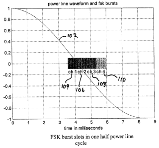
[0024] Figure 1 a is a graph of exemplary FSK burst slots in one half power
line cycle
produced by an embodiment;
[0025] Figure lb is another view of the FSK burst slots of Figure la;
[0026] Figure 2 is a block diagram of correlation receiver for a two frequency
FSK of
the embodiment related to Figure 1 a;
[0027] Figure 3 is block diagram of an analog front end (AFE) of an embodiment
related to Figure 1 a;
[0028] Figure 4 is a schematic diagram of a transmitter circuit of the AFE of
Figure
3;
4
TDO-RED #8312440 v. 1
CA 02539884 2006-03-16
[0029] Figure 5 is a schematic diagram of a low pass filter of the AFE of
Figure 3;
[0030] Figure 6 is a schematic diagram of a high pass filter of the AFE of
Figure 3;
[0031] Figure 7 is a schematic diagram of a protection circuit of the AFE of
Figure 3;
[0032] Figure 8 is a schematic diagram of a band pass filter and amplifier of
the AFE
of Figure 3;
[0033] Figure 9 is a schematic diagram of a high pass filter of the AFE of
Figure 3;
[0034] Figure 10 is a schematic diagram of a protection diode circuit of the
AFE of
Figure 3;
[0035] Figure 11 is a schematic diagram of a band pass filter and amplifier of
the
AFE of Figure 3;
[0036] Figure 12 is a schematic diagram of another low pass filter of the AFE
of
Figure 3;
[0037] Figure 13 is a schematic diagram of another band pass filter and
amplifier of
the AFE of Figure 3;
[0038] Figure 14 is a schematic diagram of a limiter of the AFE of Figure 3;
[0039] Figures 15a and 15b are schematic diagrams of an automatic gain control
amplifier of the AFE of Figure 3;
[0040] Figure 16 is chart showing an optimized reception and transmission of
multiple frequencies using a sine wave for the embodiment of Figure 3;
[0041] Figure 17 is a graph showing a spectral density graph of signals
processed by
the embodiment of Fig. 3;
[0042] Figure 18 is a block diagram of another analog front end (AFE) of
another
embodiment connected to a microcontroller;
[0043] Figure 19 is a flow chart of a zero-crossing algorithm used by the AFE
of
Figure 18;
[0044] Figure 20 is a voltage-time graph of a set of signals processed by the
AFE of
Figure 18;
TDO-RED #8312440 v. 7
CA 02539884 2006-03-16
[0045] Figure 21 is a flow chart of a receive window signal algorithm
implemented
by the AFE of Figure 18;
[0046] Figure 22 is a block diagram of a merged channels algorithm implemented
by
the AFE of Figure 18;
[0047] Figure 23 is a signal magnitude calculation formula used by the AFE of
Figure 18;
[0048] Figure 24 is a collection of tables of frequency values and associated
bit
codings used by the AFE of Figure 18;
[0049] Figure 25 is a voltage-time graph of a set of signals generated by a
differential
bit encoding algorithm used by the AFE of Figure 18; and
[0050] Figure 26 is a block diagram of an exemplary processing of signals in a
six (6)
window arrangement for the zero-crossing algorithm of Figure 19 used by the
AFE of
Figure 18.
DETAILED DESCRIPTION OF EMBODIMENTS
[0051] The description which follows, and the embodiments described therein,
are
provided by way of illustration of an example, or examples, of particular
embodiments of
the principles of the present invention. These examples are provided for the
purposes of
explanation, and not limitation, of those principles and of the invention. In
the
description, which follows, like parts are marked throughout the specification
and the
drawings with the same respective reference numerals.
[0052] Briefly, a signal transmission system and method related to an
embodiment of
the present invention uses both time and frequency diversity in the
transmitted signal to
improve the robustness of the system. The robustness is improved notably in
the
presence of large amounts of non-stationary power line noise. As such, the
embodiment
achieves significantly improved performance in very adverse conditions.
[0053] In an aspect of the embodiment, the transmission system divides the
time axis
into a number of time slots synchronized such that one time slot starts at the
zero crossing
of an alternative current (AC) power line signal (50 or 60 Hz depending on the
region).
6
TDO-RED #8312440 v. 1
CA 02539884 2006-03-16
These time slots are called channels and numbered from 1 to n. For the
embodiment, the
notion of a channel and a timeslot may be used interchangeably. However, if
necessary,
the terms can be used to mean different concepts. In particular, a channel can
be thought
to be a logical boundary while a time slot can be a specific implementation of
the
channel. The modulation method preferably used is narrow band continuous phase
FSK,
where a number m of modulating frequencies are used, arranged such that an
integral
number of full cycles fit into each channel time slot for all m frequencies.
The system
transmits during only a subset of the available time slots (channels)
concentrated near the
zero crossing of the power line waveform where the noise is typically minimal.
In
addition the initial phase of the individual frequencies may be varied (from
zero going
positive to zero going negative). This allows differential reception where
only the
difference in energy between two bursts is used instead of the actual value,
leading to
further robustness in the presence of noise.
[0054] The different channels may be used to transfer data to different
clients at the
same time. In addition they may also be combined to provide diversity as
outlined
below.
[0055] The system can use diversity of signal transmissions by transmitting
the same
bit over one or more channels (time slots) and one or more frequencies as well
as one of
the two phases. It uses a positive acknowledgment protocol with a reverse
channel to tell
the transmitter which redundancy method to use at any given time. The
transmitter and
receiver are both synchronized to the power line signal zero crossing and the
default
transmission method is the lowest bit rate using the maximum diversity. The
system
preferably uses a cyclic redundancy check (CRC) polynomial to detect the
correct
reception of messages. If the CRC is not received correctly, no acknowledgment
is sent
and the transmitter will revert to its default high redundancy state after
some
programmable delay.
[0056] In the descriptions that follow, an embodiment of the system is
described
using a particular example of 4 channels and 2 frequencies on a 60 Hz power
line.
However it should be clear to anyone versed in the art that this can be
readily changed to
7
TDO-RED #8312440 v. I
CA 02539884 2006-03-16
a n channels and m frequencies as well as the use on other power line
frequencies (e.g. 50
Hz), in other embodiments.
Burst mode FSK
[0057] For the embodiment, one transmission method that can be used is
traditional
FSK with two frequencies. Referring to Figures 1 a and lb, a power wave 102 is
shown.
The period of the power line waveform is divided into a number of segments and
transmission of data occurs during some but not all these segments. Thus
consider
segments of 600 ,sec - in a 60 Hz power line the period is 16.67 msec and the
half period
is 8.33 msec, giving 14 time slots of 595 sec in one half period. Of these the
system
transmits in four (4) timeslots of 595 .sec, leaving the rest of the period
empty. The four
timeslots are arranged asymmetrically with one before the zero crossing and
three after,
as illustrated in Figures la and lb. The timeslots are numbered as channels 1
to 4. The
exemplary signals shown in Figure 1 correspond to the simplest case where no
redundancy is used. The channels 104 and 108 are modulated with frequency 1
and
coded as 0, while the channels 106 and 110 are modulated at frequency 2 and
coded as 1.
The data representing bit pattern is 0101 and is transmitted during this one
burst.
[0058] The system of the embodiment uses continuous phase FSK with the
transmitted signals:
Sm (t) _ ~ cos(2~ f~t + 2~z m Of t) m =1,2
and 0f chosen such that:
of-k
T
which provides seamless switching at the end of the burst T. Choosing T = 600
sec and:
8
TDO-RED #83J2440 v, I
CA 02539884 2006-03-16
_70 =116.7 kHz
f = f~ = T
0f=~=16.7kHz
f2=f,+0f=133.3 kHz
completes the definition of the bursts. The receiver uses a bank of
correlators as shown
in Figure 3. The correlators are synchronized to the zero crossing of the
power line
waveform and the output is sampled at the nearest peak at the end of the
period T,
minimizing the effect of any fitter in the zero crossing detection.
[0059] Referring to Fig. 2, cross-correlation of these signals sampled at T is
provided
by:
Pmk - 1 l ''Sm (t)sk (t) dt
2 ..UUE
2E T T cos(2~ f~.t + 2~c mOf t) ~ ~ cos(2~c f~t + 2~c kOf t) dt
0
[0060] Referring to Figure 2, an exemplary matched-filter receiver for FSK
waveforms is shown. In the upper branch the input signal 202 ( r(t) ) is
multiplied by the
first FSK frequency reference s, (t) in the multiplier 204 and the result is
integrated in the
integrator 208 over a full period T. The resulting signal is sampled by 212,
scaled by
adder 216 and fed to the decision circuit 220.
[0061] In the lower branch the input signal 202 ( r(t) ) is multiplied by the
second
FSK frequency reference sz (t) in the multiplier 206 and the result is
integrated in the
integrator 210 over a full period T. The resulting signal is sampled by 214,
scaled by
adder 218 and fed to the decision circuit 220.
[0062] The decision circuit 220 chooses the larger of the two signals fed to
it, making
the decision that if the result of adder 216 is greater than the result of
adder 218 then
signal s, (t) was sent, otherwise making the decision that signal s2 (t) was
sent.
9
TDO-RED #8312440 v. I
CA 02539884 2006-03-16
[0063] This equation has two parts, one part at DC and the other part at twice
the
carrier frequency f~ . The result of the integration of the two parts is:
_ ~ ~cos(2~c( m - k)Of t) dt
P",k
0
+ ~ f cos(4~ f~t + 2~ (m + k)Of t) dt
0
- sin(2~( m - k)Of T ) + sin(4~c f~T + 2~c (m + k)Of T )
2~( m - k)Of T 4~ f~.T + 2~t (m + k)Of T
=1 if m=k
= 0 otherwise
where f~ ' T = 70 and 0f ' T =10 . Note that this correlation is normalized to
1 by
dividing the value by the signal power. This correlation also indicates the
effect of fitter
in the zero crossing mentioned above. In this case the correlation is over a
shorter period,
resulting in less energy at the output. If the correlator is synchronized by
taking the
largest output sample near the end of the original burst, the effect can be
approximated as
the ratio the reduced burst length due to fitter Tredto the original burst
length T as shown
below:
Pmk = 1 ~:e~ Sm (t)Sk (t) dt
2 bE
ea
2s J T cos(2~ f~.t + 2~c mOf t) ' ~ cos(2rc f~t + 2~ kOf t) dt
0
Trey sin(2~z( m - k)OfTYed ) + sin(4~ f~T + 2~ (m + k)Of T,ed )
2~(m-k)ofT,e~ 4~ f~T+2~(m+k)ofT,e~
- TY'''' if m = k
T
= 0 otherwise
where it is assumed that TYe~, ' f~ and Tr~d ' 4f are still integers. This
indicates that a
correlation is made over an integral number of cycles of f~ and f2).
TDO-RED #8312440 v. I
CA 02539884 2006-03-16
[0064] For the case where both phases of a cosine waves are used for
modulation, the
correlation results in
pmk - 1 ~ Sm (t)Sk (t) dt
2~
2s ~ T cos(2~c f~t + 2~ mOf t + ~r) ~ ~ cos(2~ f~t + 2~ kOf t) dt
0
which gives
if
Pmk = ~, jcos(2~c( m - k)Of t + ~c) dt
0
+ ~ f cos(4~ f~.t + 2~z (m + k)4f t + ~c) dt
0
- sin(2~( m - k)~f T + ~) + sin(4~ f~.T + 2~ (m + k)Of T + rc)
2~( m - k)4f T + ~c 4~t f~T + 2~ (m + k)4f T + ~
= 0 since (m - k)Of T = integer
f~. T = integer
Transmission methods using time and frequency diversity
[0065] The four time slots may be viewed as four independent channels. Thus
signal
diversity techniques can be used to improve robustness in the presence of
noise. In
particular, both time and frequency diversities can be used by transmitting
multiple
copies on different channels and using one or two frequencies as well as one
of two
possible phases, as further explained below. Thereafter, various combining
techniques
can be used to improve the robustness of the detection.
[0066] In addition to exploiting the time, frequency and phase diversity, the
embodiment also uses a differential receive technique to improve robustness.
In this
method, rather than relying on the energy at a given frequency, phase and
time, a
combination of two energy bursts in a specific order are preferably used to
signal a bit
(e.g. a "1")-the opposite combination being used to signal the opposite bit
(e.g. a "0").
In this way, dependence on the amount of energy on the channel at a given
phase, time
and frequency is replaced by the detection of specific transitions between two
energy
bursts, further enhancing robustness on very noisy channels. Several examples
of this are
11
TDO-RED #8312440 v. I
CA 02539884 2006-03-16
given below, although this redundancy can be implemented through other
techniques by
those skilled in the art.
[0067] For the embodiment, the following transmission parameters A - E may be
used:
A. 480 bps / 2 frequencies / 1 bit per channel / 4 bits per burst.
B. 240 bps / 2 frequencies / 2 bits per burst / Channel 0 and 1 merged /
Channel 2 and 3 merged
C. 120 bps / 2 frequencies / 1 bit per burst / Channel 0 and 1 merged /
Channel 2 and 3 merged / A '0' is considered to be a transition from F 1 to
F2; and
a ' 1' is considered to be a transition from F2 to F 1
D. 120 bps / 2 frequencies / 1 bit per burst / All channel merged
E. 60 bps / 2 frequencies / 1/2-bit per burst / All channel merged / A '0' is
a
considered to be a transition from F 1 to F2; and a ' 1' is a transition from
F2 to F 1
Other methods made by used using more channels and more frequencies.
[0068] Implementation of these parameters are illustrated in Tables 1 to 5 and
described below:
Burst 1
b0 bl b3 b4
Table 1 Method A
Burst 1
b0 b0 bl bl
Table 2 Method B
Burst 1
F1 F1 F2 F2
0
F2 F2 F1 F1
1
Table 3 Method C
12
TDO-RED #8312440 v. I
CA 02539884 2006-03-16
Burst 1
b0 b0 b0 b0
Table 4 Method D
Burst Burst
1 2
F1 F1 F1 F1 F2 F2 F2 F2
0
F2 F2 F2 F2 F1 Fl F1 F1
Table 5 Method E
Detection algorithms using time, frequency and phase diversity
[0069] For the embodiment, the detector uses time and frequency diversity
methods
to improve the robustness of the transmission. The four channels and the two
frequencies
are used to make a combined decision depending on the transmitted sequence.
The
receiver monitors the channel and makes a decision on which transmission
method is
likely to yield the best result. A reverse channel protocol is used to
communicate this
decision to the transmitter.
[0070] Outlined below with reference to Tables I-5 are some of the detection
methods that can be used, although other methods may also be used as known to
those
skilled in the art. A basic feature is to use time diversity first by either
repeating the same
information in a number of time slots or by reducing the number of time slots
used by
ignoring the ones that are too noisy. The detected signal is then combined
with frequency
diversity by using only one of the two frequencies to make the decision,
ignoring the
other one judged to be too noisy. In a general case, k of n time slots are
used and 1 of m
frequencies are used.
[0071 ] Method A:
1. Use maximum likelihood decision from correlator
[0072] Method B
1. Use maximum likelihood decision from correlator on merged channels
13
TDO-RED #8312440 v. 7
CA 02539884 2006-03-16
2. Use maximum likelihood decision from correlator only on merged channels 1,2
[0073] Method C
1. Use maximum likelihood decision from correlator on merged channels 1,2 and
3,4
then apply differential decoding
2. Use maximum likelihood decision from correlator only on merged channels 1,2
then apply differential decoding
3. Same as 1 or 2 but monitor only change in F 1
4. Same as 1 or 2 but monitor only change in F2
[0074] Method D
1. Use maximum likelihood decision from correlator on merged channels 1,2,3,4
2. Use maximum likelihood decision from correlator only on merged channels 1,2
3. Use maximum likelihood decision from correlator only on channel 1
4. Use maximum likelihood decision from correlator only on channel 2
[0075] Method E
1. Use maximum likelihood decision from correlator on merged channels 1,2,3,4
in
burst 1 and burst 2 and apply differential decoding
2. Use maximum likelihood decision from correlator only on merged channels 1,2
in
burst 1 and burst 2 and apply differential decoding
3. Use maximum likelihood decision from correlator only on channel 1 in burst
1 and
burst 2 and apply differential decoding
4. Use maximum likelihood decision from correlator only on channel 2 in burst
1 and
burst 2 and apply differential decoding
5. Same as 1 to 4 but monitor only change in F 1
6. Same as 1 to 4 but monitor only change in F2
14
TDO-RED #8312440 v. I
CA 02539884 2006-03-16
Synchronization, startup and tracking
[0076] For the embodiment, the embodiment preferably uses a link layer
protocol for
startup and tracking. Synchronization is achieved by detecting the zero
crossing of the
power line signal and then looking for the maximum of the larger correlator
output to
determine the end of the burst near T microseconds after the zero crossing
(note that the
correlator will contain part of the second burst if the zero crossing is
detected late or
noise only if it is detected early due to fitter. However, the effect of this
is small as
shown above). The zero detection circuit can use any signal monitoring or
detection
circuit known to those skilled in the art. Other embodiments may use other
synchronization points for determining where to insert and expect data in the
power
signal. The zero detection circuit can be designed to trigger a
synchronization signal
when the value of the power signal is about zero, that it, approaching or near
zero volts.
[0077] The link layer protocol transmits messages bounded by a start of
message
sync pattern at the beginning and a CRC byte at the end of the message. The
receiver
uses this CRC to determine if correct operation has been achieved and sends a
positive
acknowledgement to the transmitter to that effect.
[0078] It is noted that other link layer protocols may also be used in
conjunction with
the transmission system in other embodiments, as will be evident to those
skilled in the
art.
[0079] Startup is achieved by transmitting at the lowest bit rate, ('/2 bit
per burst in
this case). Once successful transmission at this bit rate is achieved (correct
CRC
received), the receiver monitors all channels and all frequencies to determine
if a higher
bit rate could be sustained. It then communicates to the transmitter via a
control message
to use one of the other transmission patterns and switches its detection
algorithm
accordingly. It should be noted that another implementation can start with the
highest bit
rate and reduce it in case of bad CRC. Improved robustness can be provided by
positively acknowledging each message. This allows the transmitter to revert
to the
lowest bit rate in case the channel deteriorates to the point where the
receiver is not
receiving correct data and does not send an acknowledgement. For the
embodiment, this
TDO-RED #8312440 v. I
CA 02539884 2006-03-16
provides synchronisation with a frequency or frequencies so that the receiver
can receive
information from the transmitter.
Analog Front End
[0080] Referring to Fig. 3, the analog front end (AFE) is an analog circuit
composed
of a transmission circuit and a reception circuit. This circuit provides the
connection
from the digital signal processing portions of the system to the analog
portion of the
power line. The receiver circuit is always on, whereas the transmitter circuit
must be
enabled with a logical high (1) on the TX Enb pin. Both circuits have a
protection diode
circuit to limit spikes and signals present on the powerline and pass through
the coupling.
For the embodiment, the AFE is a discrete circuit separate from the
microcontroller, such
as microcontroller 1804 described below in Figure 18. However, one of skill in
this art
would appreciate that other circuit arrangements may be used in other
embodiments.
[0081] A simplified block diagram of the AFE is shown at 300. For the
embodiment,
the following provides a summary of different filters that may be used in the
AFE:
Description Value Note
Filter 1 Characteristics
Filter type Butterworth Low-Pass
Order 4
Cut off Frequency 180 KHz -3 dB
Filter 2 CharacteristicsButterworth High-Pass
Filter type
Order 2
Cut off Frequency 190 KHz -3 dB
Filter 3 Characteristics
Filter type (Type) Band-Pass
Order for the high10
pass
Order for the low 4
pass
Cut off Frequency 106 KHz -6 dB
(Low)
Cut off Frequency 160 KHz -6 dB
(High)
Frequency Center 125 KHz
Gain 20 dB
AGC Characteristics
Gain >30 dB
Response delay 305
Power Amplifier
16
TDO-RED #8312440 v. l
CA 02539884 2006-03-16
Characteristics
Input impedance 60052
Output impedance <1~
Gain 11 t 1 dB
Bandwidth 80-150 kHz
Power 2.25 Wpeak 3 Vpeak in 4S2)
Protection Short circuit and Protected by coupler
over impedance
voltage
Distortion -60 dB (3' harmonic)Output impedance:
50~
Table 6 - AFE Specifications
[0082] Details regarding different aspects of the AFE are now briefly
described
below. More details regarding AFE's is provided in U.S. Patent No. 6,727,804,
the
contents of which are hereby incorporated by reference. Referring now to
Figure 3, there
is provide an exemplary AFE 300. AFE 300 includes amplifiers 306 and 312, low
pass
filters 304 and 310, band pass filters 314 and 318, and high pass filter 316.
Connection
320 couples AFE 300 to a coupling circuit, connection 302 and 308 provides to
a power
line for transmitter and receiver circuits, as described below.
Transmitter Circuit
[0083] Referring to Figure 4, the exemplary amplifier section 400 of the AFE
is made
up of two stages:
~ The transmission filter (TX filter); and
A voltage/current stage amplifies the input signal with low-distortion to meet
FCC, ICES and CENELEC requirements. Preferably, the output stage has low
output impedance. The amplifier is controlled by the Tx Enb signal. When
Tx Enb is low, the current stage is high impedance to allow power line signal
to
be received by the RX section. When Tx Enb is high, the current stage
amplifies
the signal from the voltage amplifier and transmits it to the coupler.
[0084] The amplification is l ltl dB. As such, the range is 1.7 volts peak-to-
peak.
The output impedance is less than 1 S2 when transmitting and more than 250 S2
in idle
state. The transmitter preferably uses an integrated circuit provide the
amplification. The
17
TDO-RED #8372440 v. I
CA 02539884 2006-03-16
amplifier preferably supports low impedance on the power line without
distorting the
signal transmission.
[0085] For the embodiment, the two amplifiers 306 and 312 work with a bridge
configuration to transmit a 6 Vpp signal on the line from a single SV supply.
The output
of the transmission amplifier 306 is not protected against shorts between
ground and
output. The output signal is transmitted at 6 Vpp for a load greater than 6
S2. For a load
smaller than 6 S2, the output signal decreases, but the distortion stays at a
low level to
avoid transmitting harmonics on the power line.
[0086] The band-pass filter of the amplifier preferably has a pass range from
80 kHz
to 150 kHz. As the circuit provides a pulse width modulation signal, it is
preferably to
filter it using a passive low pass filter to reshape the signal to amplify.
The transmitting
filter is used to filter the signal taken from the circuit and to feed it to
the voltage/current
amplifier 306. This is accomplished by eliminating the high frequencies of the
TX signal
at the input of the amplifier. This may be done by a low pass filter 500 as
shown in
Figure 5. An exemplary circuit 600 for a high pass filter is shown in Figure
6.
Receiver Circuit
[0087] For the embodiment, the receiving circuit is preferably always enabled.
It
receives the signal from the power line and filters it for the circuit. The
receiver provides
the following functions:
- Extract the inbound signal of the noise present at the output of the
coupling
circuit by a efficiency filtering
- Compress the signal without clipping it to preserve the shape when the
maximum amplitude is reached
- Amplify the signal when it is necessary; depending of the attenuation
present
on the powerline
- Warn the circuit when the signal is being compressed and when the line is
noisy
18
TDO-RED #8312440 v. 1
CA 02539884 2006-03-16
[0088] To perform these functions, the receiver is divided in several sections
which
are independent of each other. Depending of performances required for
different
applications, different sections can be added and taken out of the circuit.
For the
embodiment, the following sections are available:
- A high pass filter
- A protection diode circuit
- A band-pass filter and amplifier
- A high pass filter
- A protection diode circuit
- A band-pass filter and amplifier
- A low pass filter
- A band-pass filter and amplifier
- A limner that react as a protection for the circuit
- An automatic gain control amplifier which control gain of two of the three
amplifiers
[0089] The sections preferably clean the signal, but do not saturate and
preferably
preserve the shape of the signal. The minimum signal to be detected by the AFE
is
30 pV if the noise floor is lower than -97 dB (Vpp). This gives a sensitivity
of -97 dB.
[0090] Each of the sections of the receiver circuit now described in turn.
Referring
first to Figures 6 and 9, high-pass filters 600 and 900 respectively are
shown. It will be
appreciated that each filter operates in a manner known to those skilled in
the art. It will
also be appreciated that the pass point for either filter may be set according
to operation
characteristics required by the system.
[0091] Referring to Figures 7, 10 and 14, protection circuits 700, 1000 and
1400 are
shown. Either protection circuit may clamp voltages to a predetermined level
to prevent
overloading of the circuits downstream to them. Other protection circuits may
be
provided. In particular, limiter 1400 that react as a protection for a
processing circuit.
[0092] Referring to Figures 8, 11 and 13, a band-pass filter and amplifier
circuits 800,
1100 and 1300 respectively are shown. It will be appreciated that each band-
pass filter
19
TDO-RED #8312440 v. 1
CA 02539884 2006-03-16
operates in a manner known to those skilled in the art. It will also be
appreciated that the
pass points for each filter may be set according to operation characteristics
required by
the system. Each amplifier operates to amplify the output signal of the band-
pass filter.
The level of amplification can be designed to meet operation characteristics
required by
the system.
[0093] Referring to Figure 12, a low pass filter 1200 is shown. It will also
be
appreciated that the pass point for the filter may be set according to
operation
characteristics required by the system.
[0094] Referring to Figures 15a and 15b, an automatic gain control (AGC)
amplifier
1500a and 1500b that controls gain of two of the three amplifiers are shown.
The AGC is
designed to have fast response within 805. This is enough fast to control
amplification
of the different section of the receiver and gives feedback to the circuit.
[0095] Referring now to Figure 16, an optimized reception and transmission of
multiple frequencies using a single sine wave is now described and shown in
graph 1600.
As shown, there is a 356 point 2.5 kHz sine wave stored in RAM memory (for a
sampling
rate of 888888.8 samples per seconds). This single sine wave is used by the
DSP to
perform discrete time Fourier transfer (DTFT) on any frequency that is a
multiple of 2.5
kHz.
[0096] The following function performs the DTFT at 110 kHz using this table.
It is
noted that only N register needs to be modified in order to select any
frequency:
moveu.w #356,LC // 2c
moveu.w #(32768 + 356-1 ), MO1 // RO and R1 are configured as MOD(356)
Addressing
move.w #44,N // 44 x 2.5 kHz = 110 kHz parameter
moveu.w #DFTTable + 89,80 // Imaginary Part (Cos) offset of 90 degrees
moveu.w #DFTTable,Rl // Real Part (Sin) no offset
moveu.w #TestBuffer,R3 // ADC Data Ptr
clr a x:(rl)+N,yl // real part + add(N) to rl
nop
clr b x:(r0)+N,yO x:(r3)+,x0 // imaginary part + add(N) to r0
DOSLC _ENDOFLOOP
mac yl,x0,a x:(rl)+N,yl // real part+ add(N) to rl
mac y0,x0,b x:(r0)+N,yO x:(r3)+,x0 // imaginary part + add(N) to r0
ENDOFLOOP:
TDO-RED #8312440 v. I
CA 02539884 2006-03-16
[0097] Referring to Fig. 17, graph 1700 shows relationships between the
various
input signals and channels. In particular, it provides a three dimensional
portrayal of the
information shown in Fig. 1. Therein, an exemplary system utilizes twelve
channels in
twelve sequential time slots [OJ, [ 1 J, [2] . . . [ 11 J. In other
embodiments, more or less slots
can be used. Data is encoded in the channels around the zero crossing of the
AC signal.
These are shown in burst signals shown grouped as blocks of signals 1702, 1704
and
1706. Each burst signal includes data encoded in each of the 12 channels. The
peak
signal in each channel in each zero crossing is the encoded data element.
Other energies
in the signal in the channel include noise and harmonics associated with the
injected
signals. The regions 1708 show less energies therein because they represent
the power
signal around non zero crossing regions and as such, no data encoded in the
power signal
at those regions.
Transmitter and Receiver Circuit
[0098] Referring now to Figures 18-26 aspects of another embodiment are shown.
In
particular, a complementary transmit and receive module is described
implementing
aspects of the earlier described synchronization, transmission and reception
techniques.
[0099] Figure 18 shows system 1800, where AFE 1802 receives analog signals
from
and inserts data in the signals on powerline 1806. Powerline 1806 is the
medium over
which data may be exchanged through its power signals. Microcontroller 1804
provides
the modules for encoding and decoding data from the power signals using
systems and
methods described herein. Software operating on microcontroller 1804 is stored
in a non-
volatile memory location (not shown) and controls operation of the
microcontroller in
how it processes information and data received and sent to the AFE 1802.
Referring to
Figure 20, at initialization, transmitters and receivers synchronize
themselves by the
means of the powerline 2002 having zero-crossings 2006, 2008. The zero-
crossing 2006,
2008 point of the powerline 2002 is used to estimate where a "burst" to be
transmitted by
the transmitter or as to be captured by the receiver is located.
[00100] Referring again to Figure 18, on reception a data signal is received
from
powerline 1806 by the AFE 1802 by way of coupling circuit 1808. Bandpass
filter and
gain 1810 is used to filter the signal and to increase its strength. After
this stage, the
21
TDO-RED #8312440 v. 1
CA 02539884 2006-03-16
signal is routed through to the micro-controller ADC or comparator 1818 on
microcontroller 1804. The samples received are then stored to RAM 1824 as
needed.
Microcontroller 1804 can then decode data from the signal. In decoding the
data,
microcontroller can determine what channel (if any) the data came from and can
then use
the data to reconstruct an original data string, if additional data is
required from
additional channels or bursts.
[00101] On transmission, the microcontroller 1804 determines what data is to
be
encoded, what channel (if any) that the data is to be sent on and then encodes
the data
into a PWM signal via its pulse width modulator or DAC 1820. This analog
signal is
then sent to AFE 1802 and filtered in order to meet any applicable regulations
by filter
1814. Once filtered, the signal is amplified by amplifier 1812 and is
transmitted to
powerline 1806 via coupling circuit 1808 for transmission. Timing of the
insertion of the
signal can be controlled, in part, by the zero-detection circuit.
[00102] Referring to Figures 19 and 20, the zero crossing circuit implements
algorithm
1900 is shown. Referring first to Figure 19, there is an example of a zero-
crossing
synchronization shown on flowchart 1900, in which 2 timers are used and where
a
"burst" begins before the zero-crossing point. In relation to Figure 20, the
timer
described in Figure 19 is for calculating a delay between a previous zero-
crossing (such
as 2008 in Figure 20) and the current zero-crossing pulse (such as 2006 in
Figure 20). A
second timer is then loaded with this calculated value minus the "burst"
offset. This
second timer may then expire at the start of the "burst" (such as identified
as 2004 in
Figure 20) and depending on the device state, it can issue a transmission or a
reception.
This process can be repeated indefinitely.
[00103] Referring to Figure 21, the RX WindowProcessing step of chart 1900 is
shown in greater detail. As RX WindowProcessing begins, the receiver and
transmitter
are already synchronized, and synchronization is no longer an issue. The goal
of the RX
WindowProcessing is to show how various channels and frequencies can be
processed
during the "burst". This processing is performed by the microcontroller 1804
of Figure
18. The signal received is the output of the ADC or comparator 1818. At the
beginning
of a burst, the RX samples are buffered for the entire duration of the burst
at step 2102.
22
TDO-RED #8312440 v. 1
CA 02539884 2006-03-16
As such, n samples are buffered into RAM memory 1824. The burst is separated
into
many channels, where the samples are equally distributed. Once the buffering
is
complete, discrete Fourier transforms (DFTs) are calculated for each channel
and each
frequency at steps 2108-2116. For example, if there are 4 channels in each
burst and if 8
frequencies are analyzed by the receiver then 32 DFTs are performed.
[00104] Once each channel's frequency DFTs results are stored into memory, the
merged channel processing step 2118 is performed, as described in greater
detail below.
Thereafter, the calculate frequency magnitude step 2120 is performed, and
after all
magnitudes are processed at step 2120, the bit processing step is performed at
step 2122.
For the embodiment, once each channel's frequency DFTs results are stored into
memory, the merged channel processing step 2118 is performed, as described in
greater
detail below. Thereafter, the calculate frequency magnitude step 2120 is
performed.
This step is used in order to determine the relative power of each frequency
based on the
complex numbers outputted from previous steps. After all magnitudes are
processed at
step 2120, the bit processing step is performed at step 2122. This step is
used to
determine if the device is receiving Os or 1 s by comparing the various
frequency
magnitudes.
[00105] Referring to Figure 22, a block diagram of elements used to provide
merged
channel processing from step 2118 described above is shown at 2200. At this
stage, all
the signal filtering and processing has been completed, and the merged
channels
processing is no longer concerned with signal samples but rather with complex
numbers
that are the output of the DFT or FFT as described above. In the embodiment,
channel
merging is performed in order to support lower-baud rate and increase
robustness against
noise. For example, Figure 22 shows the sum of many channels can be analysed
to create
a slower process that tends to be more robust against noise.
[00106] Since the output of the DFT is a complex number, merged channel
processing
may add two channels by performing a complex addition of the complex number
DFT
output of the two channels. As there may be many frequencies per channel, a
separate
sum is performed for each frequency. The complex sum is therefore the addition
of the
23
TDO-RED #8312440 v. I
CA 02539884 2006-03-16
imaginary part of both channels to be merged and the addition of both real
parts of the
channels to be merged:
Channel 1 of 4 REAL = (Channel 1 of 8 REAL + Channel 2 of 8 REAL)
Channel 1 of 4 IMG = (Channel 1 of 8 IMG + Channel 2 of 8 IMG)
[00107] For example, referring to Figure 22, 7 merged channels are created by
merging the 8 base channels, as shown in flow chart 2200. Seven sum operations
per
supported frequency are required to create these extended channels. It will be
appreciated that it is also possible to create other channels, for example one
can create a
merged channel by the sum of (Channel 2 of 4) and (Channel 3 of 4).
[00108] Referring to Figure 23, a formula for calculating the magnitude of the
frequency per step 2120 above is shown at 2300. As described above, the output
of the
FFTs and DFTs process from Figure 21, and the output of the channel merge
processing
in Figure 22, are expressed as a complex number for each channel by each
frequency.
For example, for a 2-frequency modulation, if there are 2 channels per burst
and 1
merged channel that is the sum of the 2 channels, the output of the processing
from
merged channel processing will be the following 6 complex numbers
Complex Number 1 (Channel 1 Frequency 1 )
Complex Number 2 (Channel 1 Frequency 2)
Complex Number 3 (Channel 2 Frequency 1 )
Complex Number 4 (Channel 2 Frequency 2)
Complex Number 5 (Sum of Complex Number l and Complex Number 3)
Complex Number 6 (Sum of Complex Number 2 and Complex Number 4)
[00109] A complex number can be expressed as a 2-dimension vector with a real
and
an imaginary part. The angle of this vector is the phase of the entry signal
for the given
frequency. The length of this vector is the power (or magnitude) of the
frequency. The
equation shown in Figure 23 is thus used to calculate the power of the
frequency based on
the complex number associated with that frequency. The magnitude of each
frequency is
also calculated in order find the frequency with the higher power.
24
TDO-RED #8372440 v. l
CA 02539884 2006-03-16
[00110] Referring to Fig. 24, a set of tables indicating how frequencies are
mapped to
bit codings are shown, per step 2122 described above. The input of the process
bit
processing step is a magnitude for every channel and frequency. With this
magnitude of
each frequency one can determine which frequency was most likely transmitted
by the
transmitter device (i.e., the frequency with the highest magnitude) in
relation to FSK
demodulation, as described above.
[00111] The tables of figure 24 set out an exemplary bit coding for each
frequency,
depending on the number of frequencies supported by the devices. Another
example of a
table showing another set of frequencies is shown below:
Frequency Bit
in kHz
Frequency(example) Coding
#
0 100 OOOOb
1 105 0001b
2 110 0010b
3 115 0011b
4 120 0100b
125 0101b
g 130 0110b
7 135 0111b
g 140 1000b
g 145 1001b
150 1010b
11 155 1011b
12 160 1100b
13 165 1101b
14 170 1110b
175 1111b
Frequency
in kHz Bit
Frequency(example)Coding
#
0 100 OOOb
1 110 001b
2 120 010b
3 130 011b
4 140 100b
5 150 101b
g 160 110b
7 170 111b
TDO-RED #8312440 v. I
CA 02539884 2006-03-16
[00112] Additionally, another example of bit coding for a differential bit
receiver is
shown below:
Burst 0 Burst 1
Frequency Frequency
in kHz in kHz Bit
Frequency # (example) Frequency # (example) Coding
0 100 1 110 Ob
1 110 0 100 1b
[00113] Referring to Figures 25 and 26, an example of differential bit coding
processing for a signal is provided. Figures 25 and 26 show an example of a
differential
bit coding transmission. Figure 25 shows 6 bursts required to transmit '011'
on the
medium, as shown at 2500. Figure 26 shows a graph 2600. For each bit, 2 bursts
are
required. A '0' requires a 100 kHz burst followed by a 110 kHz burst while a
'1' requires
a 110 kHz burst followed by a 100 kHz burst. The bursts 1 to 6 are mapped to
time into
the figure 26. The bursts are synchronized with the powerline (see for
example, Figure
18 section 1806) and zero-crossings (see for example, Figure 18, section 1816
and 1822).
[00114] It will be appreciated that the same principles may be used in
transmission in
order to generate a pulse width modulated wave.
[00115] The embodiments above have described systems and methods for encoding
data into AC signal in timeslots about a zero crossing of the AC signal. It
will be
appreciated that in other embodiments, other predetermined points) of the AC
signal
may be used. For example, a peak/trough detect circuit can be used and the
data may be
inserted at or near a peak/trough value of the signal. Alternatively the data
can be
inserted at a predetermined offset from the peak/trough value.
[00116] Further still, in other embodiments, data may be inserted in non-AC
signals.
Such DC-based signals may be provided, for example, on twisted pair
transmission lines.
[00117] Although the invention has been described with reference to certain
specific
embodiments, various modifications thereof will be apparent to those skilled
in the art
without department from the scope of the invention.
26
TDO-RED #8312440 v. I