Note: Descriptions are shown in the official language in which they were submitted.
CA 02540219 2006-03-17
Shapiro Cohen No.: 1763P03CA01
PATCH RADIATOR
FIELD OF THE INVENTION
The present invention relates to antenna elements
and in particular to patch radiators in beamformed antenna
elements.
BACKGROUND TO THE INVENTION
In beamformed or steerable antenna systems, such
as may be used in base stations for cellular telephone
networks, an antenna may be comprised of an array of
identical antenna elements.
In one such design, known as a cavity backed,
slot fed dual polarized patched element, the antenna
element comprises, in order from the back of the radiating
element to the front, a cavity structure, a dual feed
network, a pair of slots and a patch radiator.
The cavity ensures that all of the radiated
energy emerges out of the front of the antenna element.
The dual feed network is largely to provide the
necessary fields to drive the patch radiator by exciting
the right field structure on the patch radiator.
The slots are used in dual polarization elements
in order to minimize any mutual coupling between adjacent
antenna elements.
1
CA 02540219 2006-03-17
Shapiro Cohen No.: 1763P03CA01
The patch radiator is the active or radiating
part of the antenna element. The size and configuration of
the patch radiator has a significant impact on the
operating characteristics of the antenna element.
However, in beamformed antenna arrays, the
spacing between the centres of adjacent rows and/or columns
imposes a performance constraint. For example, those
skilled in the relevant art will understand that exceeding
array spacing threshold maxima may introduce grating lobes
in the radiated signal, which is generally undesirable. As
an exemplary rule of thumb, array elements may be
restricted to no more than 0.5 wavelength spacing in the
azimuthal plane and 0.8 wavelength spacing in the elevation
plane. The greater wavelength spacing in the elevation
plane is generally considered acceptable because typically
the narrow beamwidth and low skew angle of the beam
provides assistance so that the undesirable grating lobes
cannot form.
Leaving aside the performance implications, it is
generally desirable to optimize the array element spacing
so as to produce an antenna array with a smallest physical
footprint consistent with the required radiation patterns.
Therefore, care must be taken to design a patch
element that provides satisfactory performance while
satisfying the various design criteria of the radiating
element. For example, it is generally accepted that for
dual polarization elements, the two polarizations are set
at +/- 45 . This generally implies that a square patch
radiator must be oriented along a diagonal relative to the
array.
2
CA 02540219 2006-03-17
Shapiro Cohen No.: 1763P03CA01
As well, the antenna element must be designed to
provide a suitable frequency bandwidth to accommodate the
application for which it is intended.
It is generally understood that, at least in a
colloquial or empirical sense, if not strictly proven by
electro-magnetic field calculations, and for patches that
are defined by polygonal shapes that have no interior
angles of less than 180 , the operating frequency is
determined by perimeter of the patch element. Thus, in
order to minimize physical size of the patch, it is
generally preferable to maximize the area enclosed relative
to the enclosing perimeter. As such, typical patch shapes
that have been successfully employed include square or
rectangular patches. Other patch shapes include circular
patches.
It is also generally understood in the empirical
sense at least, that the EM characteristics of such patches
impose, as a design objective, that the patch perimeter may
be in the order of 1.5 wavelengths in length.
On the other hand, it has been found that
removing some patch material from the interior of the patch
shape has an ameliorating effect on its EM characteristics
such that, as a rule of thumb, the patch perimeter may be
reduced to be in the order of 1.0 wavelengths in length.
Clearly, this has salutary benefits for the antenna
designer, who is constrained to minimize, so far as
possible, the inter-element spacing of the antenna array.
This latter observation has resulted in a second
generation of patch radiators, wherein the interior annular
3
CA 02540219 2006-03-17
Shapiro Cohen No.: 1763P03CA01
region of the patch element adopts the shape of the
exterior perimeter so that the amount of material between
the inner annular region and the exterior perimeter remains
constant. Thus, for example, an exemplary annular patch
radiator might be a square with a corresponding square
interior annular region of removed conductive material. For
this class of annular patches the centre frequency is known
to be inversely proportional to the median perimeter of the
patch with the upper and lower frequency limits
proportional to the inner and outer perimeters
respectively. Another example might be a patch of circular
shape, with an interior circular annular region of removed
material.
SUMMARY OF THE INVENTION
Accordingly, it is desirable to provide a patch
radiator configuration that maximizes upper frequency limit
and simultaneously minimizes the lower frequency limit.
It is further desirable to provide a patch
radiator configuration that is compact so as to facilitate
other antenna design constraints.
The present invention accomplishes these aims by
providing an annular patch configuration in which the
interior region of removed material is different from the
shape of the exterior perimeter.
While this introduces a difference in the amount
of material in the radiator as one proceeds along the
exterior of its perimeter, it has been found, as an
4
CA 02540219 2006-03-17
Shapiro Cohen No.: 1763P03CA01
empirical relation, that the threshold upper frequency
limit tends to increase in proportion to the ratio of the
area of removed material defined by the interior annular
region to the perimeter of such interior annular region.
Put another way, the upper frequency limit
threshold tends to rise as the interior annular perimeter
is reduced.
Those having ordinary skill in this art will
recognize that the proportion of enclosed area as a
function of a (regular) perimeter generally increases with
the number of equal length sides. Theoretically,
therefore, a circle maximizes the enclosed area as a
function of its perimeter, while a triangle minimizes its
enclosed area as a function of perimeter.
Preferably, the exterior and interior perimeters
have no interior angles of more than 180 . More
preferably, the exterior and interior perimeters are
regular polygons, that is, polygons that have sides of
equal length and equal angles.
However, because the patch element is to be used
for a dual polarized antenna element, it would be
preferable if the polygon exhibited orthogonal axes. Thus,
the smallest suitable polygon may be the square.
Accordingly, one exemplary configuration of a
suitable patch element comprises a square exterior shape,
enclosing a central circular region of removed material.
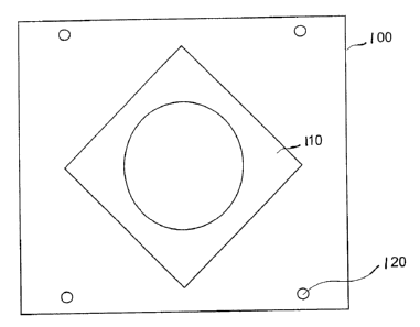
The general arrangement of the patch element is
shown in Fig. 1. The patch element 110 is printed on a
CA 02540219 2006-03-17
Shapiro Cohen No.: 1763P03CA01
supporting board structure 100 mounted over antenna
elements via mounting holes 120, and which may be
manufactured using a variety of materials such as foam,
sheet or composite dielectric materials.
Suitable foam dielectrics may include
polystyrene, polyurethane, or a mixture thereof. Suitable
sheet dielectrics may include polystyrene, polycarbonate,
Kevlar , Mylar or mixtures thereof. Suitable composite
dielectrics may include Duroid , Gtek , FR-4 , or mixtures
thereof. Alternative support structures would be known to
practitioners of the art, and could be substituted.
Printed or bonded on this support material is the patch
element 110 which may be made of conductive materials such
as copper, aluminum, or silver. It may also be printed
using suitable high conductivity inks.
It appears that the performance of the patch
improves with the conductivity of the patch material.
Thus, preferably the patch element is made out of a planar
conductive material such as copper sheeting.
Alternatively, the patch element may be
constructed out of a non-conductive printable material,
such as polycarbonate, on which a pattern corresponding to
the shape of the patch element is silkscreened, preferably
using a highly conductive ink such as a silver loaded ink
in order to reduce manufacturing cost and to increase
production. Other inks of varying conductivities could
also be used such as, gold-loaded ink, tin-loaded ink,
aluminum-loaded ink, brass-loaded ink or mixtures thereof,
as would be known to a person skilled in the art.
6
CA 02540219 2006-03-17
Shapiro Cohen No.: 1763P03CA01
According to a broad aspect of an embodiment of
the present invention, there is disclosed a conductive
patch radiator for an antenna element of an antenna array,
comprising an annular region of planar conductive material
defined by an exterior perimeter surrounding an interior
perimeter contacting a support structure of a dielectric
material, wherein the exterior perimeter of the radiator is
large relative to the area of the region enclosed thereby,
and wherein the interior perimeter of the radiator is
small relative to the area of the region enclosed thereby.
According to a further broad aspect of an
embodiment of the present invention, there is disclosed a
patch radiator for an antenna element of an antenna array,
comprising an annular region of planar conductive material
defined by an exterior perimeter surrounding an interior
perimeter contacting a support structure of dielectric
material, wherein the interior perimeter has a
configuration which is different from that of the exterior
perimeter.
Other embodiments consistent with the present
invention will become apparent from consideration of the
specification and the practice of the invention disclosed
therein.
Accordingly, the specification and the
embodiments are to be considered exemplary only, with a
true scope and spirit of the invention being disclosed by
the following claims.
7