Note: Descriptions are shown in the official language in which they were submitted.
CA 02540608 2006-03-29
1
Magnetic tunnel junction device and writing/reading method for said
device
Background of the invention
The invention relates to a magnetic device successively comprising
- a first electrode,
- a magnetic turn.' junction cunn.Qi,,eiy comprising a first
magnetic layer forming a reference layer and having a fixed
magnetization, an electrically insulating layer forming a tunnel
barrier and a second magnetic layer forming a storage layer and
having a reversible direction magnetization,
- an intermediate layer,
- and a second electrode.
State of the art
The document FR 2832542 describes a magnetic device with a magnetic
tunnel junction and methods for reading and writing using this device. As
represented in figure 1, the tunnel junction successively comprises a first
magnetic layer forming a reference layer 1 and having a fixed magnetization
2, an electrically insulating layer forming a tunnel barrier 3 and a second
magnetic layer forming a storage layer 4 and having a reversible direction
magnetization 5, represented by the two-way arrow in figure 1. The reversible
direction magnetization 5 of the storage layer 4 can be oriented with respect
to the fixed magnetization 2 of the reference layer 1 so that the
magnetizations are parallel or anti-parallel.
CA 02540608 2006-03-29
2
The blocking temperature of magnetization of the storage layer 4 is lower
than the blocking temperature of the reference layer 1. The device also
comprises a current source 6, a switch 7 and means (not shown) to apply a
magnetic field to the storage layer and to thus orient the magnetization 5 of
the storage layer 4 with respect to the magnetization 2 of the reference layer
1 without modifying the orientation of the magnetization 2 of the reference
layer 1.
In 2 write phase, i.e. in 2 magnetization phase of the storage layer 4 by
application of an external magnetic field, an electric current I is made to
flow
through the tunnel junction to heat the storage layer 4 above the blocking
temperature of its magnetization 5.
In a read phase, the orientation of the magnetization 5 of the storage layer 4
with respect to that of the reference layer 1 is measured by means of the
resistance of the magnetic tunnel junction, which depends on the orientation
of the magnetization 5 of the storage layer 4 with respect to that of the
reference layer 1.
During writing, a voltage of about 0.5 V is applied to the terminals of the
junction, requiring a relatively high electric power. The junction can
moreover
be damaged by this power. The voltage applied for reading is typically 0.3V.
The tunnel junction is then also heated during reading, which increases the
risk of unscheduled reading.
Figure 2 represents the potential energy 8 of the electrons in a tunnel
junction subjected to a potential difference V. The junction is formed by an
electron-emitting layer and an electron-receiving layer, arranged on each
side of the tunnel barrier placed at XO and respectively having an upper
Fermi level Efs and a lower Fermi level Efi. The difference of the Fermi
levels
is proportional to the potential difference: Efs-Efi=eV, e being the
elementary
CA 02540608 2006-03-29
3
charge of the electron. As illustrated by the arrow 9, an electron emitted by
the emitting layer passes through the tunnel barrier, by tunnel effect,
without
dissipating energy. Then, when inelastic relaxation of the electron from a
higher energy Efs to a lower energy Efi takes place, the electron dissipates
the energy eV in the electron-receiving layer, for example by creation of
phonons 10 and/or magnons 11, which increases the temperature of the
electron-receiving layer. Inelastic relaxation takes place over a
characteristic
length, the mean inelastic free travel kin, which length is typically about a
few
nanometers in the magnetic materials usually used in magnetic tunnel
junctions. Heat production by the tunnel current is thus maximal in a zone
with a thickness of a few nanometers, located in the receiving layer and
adjacent to the tunnel barrier.
The tunnel junction described in the document FR 2832542 can also
comprise an anti-ferromagnetic layer, for example made of NiMn, arranged
on an opposite face to the tunnel barrier of the reference layer of the tunnel
junction. Furthermore, an anti-ferromagnetic layer, for example made of
FeMn or Ir20Mn80, can also be arranged on an opposite face to the tunnel
barrier of the storage layer of the tunnel junction. The anti-ferromagnetic
layers perform the function of preserving the magnetic orientation of the
storage and reference layers. Deposition of the layers forming the tunnel
junction on the anti-ferromagnetic layer and nano-structuring of the junctions
may require additional steps, for example an alignment step. In addition, the
risk of a tunnel barrier short-circuit is increased.
The document W000/79540 describes a magnetic memory formed by a
stacking of thin layers. The document proposes to thermally insulate memory
cells to enable a Curie temperature to be achieved with a reduced electric
heating current, in particular by means of a thermal insulation layer having a
sufficient electric conductivity while having a low thermal conductivity with
CA 02540608 2012-09-05
4
respect to aluminium. The material of the thermal insulation layer is for
example a tantalum and nitrogen compound (TaN) or tungsten (W).
However, introducing such a thermal insulation layer presents additional
integration problems with the tunnel junction, i.e. an increase of the surface
roughness and an increase of the etching time necessary to define the
memory dot. Such a thermal insulation layer would require additional
polishing and etching steps, which complicate the deposition and fabrication
process of the junction.
Object of the invention
It is an object of the invention to remedy these drawbacks and, in particular,
to achieve a device enabling the storage layer to be heated efficiently while
minimizing the electric power necessary for this heating, so as to reduce the
electric consumption of the device, and to minimize the risk of a tunnel
junction short-circuit while at the same time simplifying the fabrication
method.
It is an object of the invention to provide a magnetic device comprising in
succession a first electrode, a magnetic tunnel junction comprising in
succession
a first magnetic layer forming a reference layer and having a fixed
magnetization,
an electrical insulating layer forming a tunnel barrier and a second magnetic
layer
forming a storage layer and having a reversible direction magnetization, an
intermediate layer, and a second electrode, wherein the intermediate layer is
nonmagnetic and constitutes a first thermal barrier comprising a material
having a
thermal conductivity lower than 5 W/m/ C
CA 02540608 2012-09-05
It is a further object of the invention to provide a method for read/write of
a
magnetic device according to the invention,
a write phase comprising flow of an electric current, through the
tunnel junction, from the second magnetic layer to the first
magnetic layer, so as to heat the second magnetic layer to a
higher temperature than the blocking temperature of the
magnetization of the second magnetic layer,
and a read phase comprising flow of an electric current, through
the tunnel junction, from the first magnetic layer to the second
magnetic layer.
It is also an object of the invention to provide a magnetic device comprising
in
succession a first electrode, a magnetic tunnel junction comprising in
succession
a first magnetic layer forming a reference layer and having a fixed
magnetization,
an electrically insulating layer forming a tunnel barrier and a second
magnetic
layer forming a storage layer and having a reversible direction magnetization,
an
intermediate layer, and a second electrode, wherein the intermediate layer
constitutes a first thermal barrier comprising a material having a thermal
conductivity lower than 5 W/m/ C and wherein the first thermal barrier
comprises
an anti-ferromagnetic layer, and a magnetically decoupling layer between the
first
thermal barrier and the second magnetic layer.
It is also an object of the invention to provide a magnetic device comprising
in
succession:
a first electrode;
a magnetic tunnel junction, the magnetic tunnel junction comprising in
succession a first magnetic layer forming a reference layer and having a fixed
magnetization, an electrically insulating layer forming a tunnel barrier and a
second magnetic layer forming a storage layer and having a reversible
direction
magnetization;
CA 02540608 2012-09-05
5a
an intermediate layer, wherein the intermediate layer comprises a nonmagnetic
layer or a magnetically decoupled layer associated with an antiferromagnetic
layer, and constitutes a thermal barrier formed by a material having a thermal
conductivity lower than the thermal conductivity of each of the layers in the
magnetic tunnel junction, and
a second electrode.
Brief description of the drawings
Other advantages and features will become more clearly apparent from the
following description of particular embodiments of the invention given as non-
restrictive examples only and represented in the accompanying drawings, in
which:
Figure 1 represents a device comprising a magnetic tunnel junction
according to the prior art.
Figure 2 represents the energy variations of the electrons in a tunnel
junction
according to the prior art, subjected to a potential difference.
Figures 3 to 5 represent three particular embodiments of a magnetic device
according to the invention.
Figure 6 represents two theoretical temperature distributions in a magnetic
tunnel junction, respectively for a current flowing from the storage layer to
the
reference layer and in the opposite direction.
Figures 7 to 9 represent different theoretical temperature distributions and
correspond respectively to the embodiments represented in figures 3, 4 and
5.
CA 02540608 2006-03-29
6
Description of particular embodiments
A magnetic device according to the invention comprises first and second
electrodes between which a tunnel junction such as the one represented in
figure 1 is arranged, a thermal barrier formed by a material having a low
thermal conductivity being in contact with at least one of the magnetic layers
of the tunnel junction so as to concentrate the heat produced by the tunnel
current in the storage layer during the write phases.
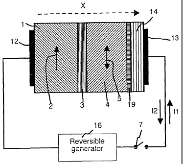
In figure 3, the device magnetic successively comprises, along an axis X, the
first electrode 12, a tunnel junction such as the one represented in figure 1,
a
first thermal barrier and the second electrode 13. The first thermal barrier
is
formed by an intermediate layer 14 arranged between the storage layer 4
and the second electrode 13. The electrodes 12 and 13 are at ambient
temperature and enable the tunnel junction to be cooled after the write and
read phases.
According to the invention, the intermediate layer 14 forming the first
thermal
barrier is formed by a material having a thermal conductivity of less than
5W/m/ C. Deposition, on an intermediate layer 14, of the layers forming the
tunnel junction is in fact simpler the smaller the thickness of the
intermediate
layer 14. In particular, the roughness of a thin layer 14 is generally lesser
and
the risk of short-circuit of a tunnel junction deposited on a thin layer 14 is
reduced. However, for a predetermined thermal resistance, the intermediate
layer 14 can present a smaller thickness the lower its thermal conductivity.
The compounds used in the prior art are not satisfactory in this respect. This
is in particular the case of the tantalum and nitrogen compound (TaN) or of
tungsten (W) mentioned in the above-mentioned document W000/79540,
which respectively have a thermal conductivity of about 35W/m/ C and of
about 173W/m/ C. This is also the case of the anti-ferromagnetic layers
CA 02540608 2006-03-29
7
made of FeMn or Ir20Mn80 mentioned in the above-mentioned document FR
2832542, which respectively have a thermal conductivity of 44 W/m/ C and
35.6 W/m/ C. The use of anti-ferromagnetic layers as thermal barrier would
require a large thickness, which would make deposition of the layers forming
the tunnel junction on the anti-ferromagnetic layer and nano-structuring of
the
junctions more difficult.
In addition, the materials having a thermal conductivity of less than 5W/m/ C
also PrIPbIr. n low thermal capacitance of the thermal barrier to be obtained,
which enables a very low thermal time constant to be obtained. The thermal
time constant corresponds to the product (Rth.Cth) of the thermal resistance
Rth of a thermal barrier and of the thermal capacitance Cth of the thermal
barrier. The lower the thermal time constant, the quicker a thermal gradient
can be established in a write phase,.
In figure 4, in addition to the first thermal barrier, the device comprises a
second thermal barrier formed by a layer 15 arranged between the first
electrode 12 and the reference layer 1.
The storage layer 4 can be formed by a single layer of magnetic material or
by a multilayer, the coercive field whereof decreases rapidly when the
temperature is increased, in a temperature interval comprised between 20 C
and 250 C. For example, the material of the storage layer can be a terbium
(Tb) and cobalt (Co) alloy enriched with cobalt near the interface between the
storage layer 4 and the tunnel barrier 3, which enables the polarization of
the
electrons passing through the tunnel barrier 3 to be increased. The Tb and
Co alloy has a blocking temperature close to the ambient temperature. The
storage layer 4 can also be formed by a repetition multilayer with a
magnetization perpendicular to the plane of the layers, for example by an
alternation of two layers of cobalt (Co) and platinum (Pt), respectively
having
a thickness of 0.5nm and 2nm.
CA 02540608 2006-03-29
8
Preferably, the storage layer 4 is formed by a stacking of a ferromagnetic
layer and an anti-ferromagnetic layer, for example made of an iron and
manganese compound, for example FeMn, or of an iridium and manganese
compound comprising for example 20% Ir and 80% Mn, having a blocking
temperature comprised between 130 C and 250 C.
Preferably, the first and/or second thermal barriers have an electrical
conductivity such that the electrical resistance of the thermal barrier is
o substantially lower than the electrical resistance of the tunnel barrier
3,
preferably at least by a factor ten. The thermal barrier being connected in
series with the tunnel barrier 3, the magneto-resistance signal is in fact
weaker the higher the electrical resistance of the thermal barrier.
The material of the first and/or second thermal barriers preferably comprises
at least one alloy containing at least one element chosen from arsenic (As),
antimony (Sb), bismuth (Bi), germanium (Ge), tin (Sn) and lead (Pb) on the
one hand, and containing at least one element chosen from sulphur (S),
selenium (Se), tellurium (Te), aluminium. (Al), gallium (Ga), indium (In) and
thallium (TI) on the other hand. The material of the thermal barriers can thus
be an alloy of bismuth (Bi) and tellurium (Te), for example BiTe or Bi2Te3,
which presents a relatively good electrical conductivity of about 1.75m52cm
for a very low thermal conductivity of about 1.5W/m/ C. Other examples for
the material of the thermal barriers are thallium, tin and tellurium alloys,
for
example TI2SnTe5, thallium, bismuth and tellurium alloys, for example
TI9BiTe6, strontium (Sr), gallium and germanium alloys, for example
Sr8Ga16Ge30, and strontium, europium (Eu), gallium and germanium alloys,
for example Sr4Eu4Ga16Ge30. It should be noted that the bismuth and
tellurium alloy forms part of the thermoelectric materials that often present
a
very low thermal conductivity.
CA 02540608 2006-03-29
9
The material of the thermal barriers can also be a phase change material,
able to present a crystalline phase and an amorphous phase at ambient
temperature. Typically, the amorphous state presents a high electrical
resistivity, whereas the crystalline state presents a low electrical
resistivity.
For a phase change material to be used for the first and/or second thermal
barriers, the material must be in its crystalline state. The thermal
conductivity
of phase change materials is typically less than 5W/m/ C, in the amorphous
state and in the crystalline state. For example, the germanium, antimony and
tellurium alloy P,p9q1-12-rp5 and the npv qb9Te3 respectively have thermal
conductivities of about 0.3W/m/ C and about 12W/m/ C. To obtain a layer in
a crystalline state, thermal treatment generally has to be performed. The
thermal treatment is advantageously performed before deposition of the
layers forming the tunnel junction.
The material of the first and/or second thermal barriers can also be a
material
comprising at least one alloy containing at least one element chosen from
phosphorus (P), arsenic (As) and antimony (Sb) and containing at least one
element chosen from iron (Fe), ruthenium (Ru), osmium (Os), cobalt (Co),
rhodium (Rh), iridium (Ir) and zinc (Zn), such as for example the alloys
Zn4Sb3 and CoFe4Sb12. Furthermore, the material of the first and/or second
thermal barriers can contain at least one element chosen from lanthanum
(La), cerium (Ce), praseodymium (Pr), neodymium (Nd), samarium (Sm),
europium (Eu), gadolinium (Gd), thulium (Tm), ytterbium (Yb), thorium (Th)
and uranium (U), such as for example the alloys Yb0.2Co4Sb12,
LaThFe3CoSb12, EuCo4Sb12 and EuCoSb12Ge0.5.
When the first thermal barrier is formed by a magnetic layer, for example an
anti-ferromagnetic layer, a magnetic decoupling layer 19 can be arranged
between the first thermal barrier, formed by the layer 14, and the storage
layer 4, as represented in figure 5, in order to decouple the magnetic thermal
barrier from the storage layer 4. The material of the magnetic decoupling
CA 02540608 2006-03-29
layer 19 can be a non-magnetic material chosen from tantalum, chromium,
vanadium, manganese and platinum. In the case of an anti-ferromagnetic
second thermal barrier, a magnetic decoupling between the second thermal
barrier and the reference layer is not necessary, as the magnetization of the
5 reference layer is trapped.
In the particular embodiment represented in figure 5, a third thermal barrier
is
formed by the tunnel barrier 3 itself. For example, the tunnel barrier can be
mArip of zirconium oxide (7r02) or titanium oxide
(Ti02).
10 The thermal conductivities of zirconium oxide and titanium oxide are
respectively 1.5W/m/ C and 7.4W/m/ C.
The temperature variation in a device according to the prior art was studied.
Thus, figure 6 represents two theoretical temperature distributions in a
magnetic device comprising a magnetic tunnel junction according to the prior
art, respectively for a current flowing from the storage layer 4 to the
reference
layer 1 (curve 17) and in the opposite direction (curve 18). To bring out the
symmetry of the temperature profile generated by the flow of the current, the
structure of this example was deliberately chosen symmetrical. The device
successively comprises, along the axis X, between the first electrode 12 and
the second electrode 13:
- a layer of tantalum (Ta) with a thickness of 5nm arranged in the gap
comprised between X1 and X2 in figure 6,
- a stacking of a 5nm layer of IrMn and a 3nm layer of NiFe forming the
reference layer 1 (X2-X0),
- a 0.6nm layer of alumina forming the tunnel barrier 3, represented, on
account of its thinness, by the dotted line arranged at XO,
- a stacking of a 3nm layer of NiFe and a 5nm layer of IrMn forming the
storage layer 4 (X0-X3)
- and a layer of Ta with a thickness of 5nm (X3-X4).
CA 02540608 2006-03-29
11
The device is then symmetrical with respect to the coordinate XO and does
not comprise a thermal barrier. The curves 17 and 18 are obtained for a
tunnel junction connected at these terminals to two copper electrodes kept at
ambient temperature and having a potential difference of 0.5V.
An asymmetry of the temperature distributions 17 and 18 can be observed in
figure 6. A current flowing from the storage layer 4 to the reference layer 1
(curve 17) in fact corresponds to a movement of electrons from the reference
layer 1 to the storage layer 4 (to the right in the figure), which implies a
dissipation of their energy in the storage layer 4 ((X0-X3), i.e. in a zone
located to the right of the tunnel barrier (XO), as represented in figure 2.
This
is illustrated by the amplitude of the curve 17, which is greater for values
of X
higher than XO than for values lower than XO. The curve 18 corresponds to a
movement of electrons flowing from right to left in the figure 6 and thus
creating more heat for values lower than XO.
Thus, for a given current, the current direction enables the magnetic layer 1
or 4 that is heating most to be defined in the junction. In this way, a
read/write
method of a magnetic device according to the invention can be performed. A
write phase comprises flow of an electric current 11 (figure 5), through the
tunnel junction, from the storage layer 4 to the reference layer 1, so as to
heat the storage layer 4 to a higher temperature than the blocking
temperature of the magnetization 5 of the storage layer 4, whereas a read
phase comprises flow of an electric current 12 (figure 5), through the tunnel
junction, in the opposite direction, i.e. from the reference layer 1 to the
storage layer 4. The storage layer 4 is thus efficiently heated during the
write
phases, whereas heating of the storage layer 4 during the read phases is
decreased. The currents 11 and 12 can for example be generated by a
reversible generator 16.
CA 02540608 2006-03-29
12
The temperature variation in a device according to the invention is
illustrated
in figures 7 to 9. The theoretical temperature distributions (curves K1 to K5)
represented in figures 7 to 9 are obtained for an electric current direction
from the storage layer 4 to the reference layer 1, i.e. for a movement of the
electrons from the reference layer 1 to the storage layer 4, and thus
correspond to the write phases.
The curves K1 to K5, and the curves 17 and 18, illustrate the temperature
distribution At the Pnri of a current pulse with a duration of 500ps and an
intensity of 250mA/vm2, corresponding to a product of the resistance R of the
tunnel junction and of the surface S of the tunnel junction RS=2Q1tm2. During
the duration of the pulse, the temperature of the junction increases rapidly
to
reach a permanent regime corresponding to the maximum temperature.
Then, when the current is annulled, the temperature drops back rapidly to the
ambient temperature by heat diffusion to the external electrodes 12 and 13
which act as thermostats.
The three curves K1, K2 and K3 represented in figure 7 illustrate the
variation of the temperature distributions in magnetic devices according to
figure 3 comprising different layers 14. Said magnetic devices also each
comprise a layer of tantalum arranged in the gap comprised between X1 and
X2 in figure 7 (not shown in figure 3).
Thus, the layer 14 of the magnetic device for the curve K1 is formed by a
stacking of a layer of BiTe with a thickness of 5nm (X3-X4) and of a layer of
Ta with a thickness of 5nm (X4-X5), successively arranged between the
storage layer 4 and the second electrode 13.
The layer 14 for the curve K2 is formed by a stacking of a layer of Ta with a
thickness of 5nm (X3-X4) and of a layer of BiTe with a thickness of 5nm (X4-
CA 02540608 2006-03-29
13
X5), successively arranged between the storage layer 4 and the second
electrode 13.
The layer 14 corresponding to the curve K3 is formed by a stacking of a layer
of Ta with a thickness of 5nm (X3-X4) and of a layer of BiTe with a thickness
of lOnm (X4-X6), successively arranged between the storage layer 4 and the
second electrode 13.
The use of thermal barriers does in fact enable temperatures comprised
between 100 C and 175 C to be reached in the layer magnetic (X0-X3),
which temperatures are therefore higher than the temperatures obtained in a
device according to the prior art (figure 6, curve 17, always substantially
lower than 100 C). The efficiency of the thermal barrier is all the better the
larger its thickness. Indeed, curve K3 is greater than curve K2. However, the
thickness of the thermal barrier limits the temperature decrease kinetics once
the current has been annulled.
Moreover, to reduce the electric consumption necessary for heating, the
storage layer 4 preferably has a small thickness, for example about 8nm.
The temperature distributions represented by the curves K1 to K3 are
obtained for an alumina tunnel barrier 3. As alumina is a good heat
conductor, the heat produced in the storage layer 4 is removed passing
through the tunnel barrier 3 and the reference layer 1 to the first electrode
12.
To limit this heat loss which is detrimental to the efficiency of heating, it
is
then advantageous to insert the second thermal barrier, represented in figure
4, to confine the heat in the storage layer 4 as far as possible.
The curve K4 represented in figure 8 illustrates the temperature distribution
of a device comprising a first and a second thermal barrier respectively
formed by a layer 14 and a layer 15. The layer 15 is formed by a stacking of
CA 02540608 2006-03-29
14
a 5nm layer of Ta (X7-X1) and of a 5nm layer of BiTe (X1-X2), successively
arranged between the first electrode 12 and the reference layer 1. The layer
14 is identical to the layer 14 corresponding to the curve Kl. The temperature
in the storage layer 4 (X0-X3) is about 300 C, which is therefore higher than
in the case of use of a first thermal barrier only (curve K1).
Figure 9 illustrates the temperature distribution (curve K5) obtained for a
device comprising a third thermal barrier formed by the tunnel barrier 3
itself
and n first thermal barrier formed by the layer 14. The tunnel barrier 3 is
formed by a silica layer with a thickness of 0.6nm. The layer 14 and
reference layer 1 are respectively identical to those corresponding to the
curve K2. The temperature in the storage layer 4 (X0-X3) is about 175 C
(curve K5), therefore higher than the temperature of a device having an
alumina tunnel barrier 3 (curve K2) whose temperature does not exceed
150 C. Indeed, silica has a lower thermal conductivity (1.5W/m/ C) than
alumina (36.7W/m/ C) and thus enables heat to be confined more efficiently
in the storage layer 4.
The invention is not limited to the embodiments represented. In particular,
any combination of the first, second and third thermal barriers is possible.