Note: Descriptions are shown in the official language in which they were submitted.
CA 02540723 2006-03-30
WO 2005/034149
PCT/EP2004/010615
SPHERICAL OR GRAIN-SHAPED SEMICONDUCTOR ELEMENT FOR USE
IN SOLAR CELLS AND METHOD FOR PRODUCING THE SAME;
METHOD FOR PRODUCING A SOLAR CELL COMPRISING SAID
SEMICONDUCTOR ELEMENT AND SOLAR CELL
Description:
The invention relates to a spherical or grain-shaped semiconductor element for
use
in solar cells and to a method for the production of said semiconductor
element.
The invention also relates to a solar cell having integrated spherical or
grain-
shaped semiconductor elements and to a method for the production of said solar
cell.
The invention also relates to a photovoltaic module having at least one solar
cell
having integrated semiconductor elements.
In photovoltaic cells, the photovoltaic effect is utilized in order to convert
solar
radiation energy into electric energy. Solar cells used for this purpose are
made
primarily of planar wafers in which a conventional p-n junction is realized.
In
order to produce a p-n junction and other function layers, in addition to
applying
and processing individual continuous layer surfaces, it has proven to be
practical
to apply semiconductor material in spherical or grain-shaped form since this
entails a number of advantages.
For example, when it comes to producing electronic devices, it has long since
been a known procedure to incorporate electronically active material as
particles
into a layer in order to increase the activity of the material. This is
described, for
example, in U.S. Pat. No. 3,736,476. In an embodiment disclosed therein, a
core
CA 02540723 2006-03-30
WO 2005/034149
PCT/EP2004/010615
2
and a layer surrounding the core are configured in such a way as to create a p-
n
junction. Several of the particles produced in this manner are incorporated
into an
insulating support layer in such a way that they protrude from the surface on
both
sides of the layer and can be contacted by further layers,
Moreover, German Preliminary Published Application DE 100 52 914 Al
describes a semiconductor device that is made up of a layer structure
consisting of
an electrically conductive support layer, an insulating layer, semiconductor
parti-
cles and an electrically conductive cover layer, whereby the semiconductor
parti-
cies are incorporated into the insulating layer and they touch the support
layer that
is underneath it as well as the cover layer that is above it. The
semiconductor
particles can consist, for example, of silicon or semiconductor
particles
that are coated with II-VI compounds.
The background for the use of compound
semiconductors such as copper
indium diselenide, copper indium sulfide, copper indium gallium sulfide and
cop-
per indium gallium diselenide can be found, for example, in U.S. Pat. Nos.
4,335,266 (Mickelsen et al.) and 4,581,108 (ICapur) in which this type of
semiconductor and methods for their production are described in depth. 1411-V1
compound semiconductors are also referred to below as chalcopyrites or CIS or
C1GS (Copper Indium Gallium diSelenide) semiconductors.
It is also a known procedure to configure independent spherical semiconductor
elements that constitute complete semiconductors, including the requisite elec-
trades, For example, European patent application EP 0 940 860 Al describes
using a spherical core to make a spherical semiconductor element by means of
masking, etching steps and the application of various material layers. Such
semiconductor elements can be used as solar cells if the p-n junction is
selected in
such a way that it can convert incident light into energy. If the p-n junction
is
configured in such a way that it can convert an applied voltage into light,
then the
semiconductor element can be employed as a light-emitting element.
CA 02540723 2006-03-30
PCT/EP/2004/010615
3
In view of the wide array of envisaged areas of application for such
semiconduc-
tor elements, the elements have to be completely independent components with
electrode connections that can be installed in other applications. This calls
for a
high complexity of the semiconductor elements and of the requisite production
processes. Due to the small dimensions amounting to a few millimeters on the
part
of the spherical shapes employed, the production of the spherical elements
with all
of the function layers and processing steps is very expensive.
Moreover, U.S. Pat. No. 5,578,503 discloses a method for the rapid production
of
chalcopyrite semiconductor layers on a substrate in which individual layers of
the
elements copper, indium or gallium and sulfur or selenium arc applied onto a
sub-
strate in elemental form or as a binary interelemental compound. The substrate
with the layer structure is then quickly heated up and kept at a temperature
of
350 C 662 F] for between 10 seconds and one hour.
Moreover, U.S. Pat. No. 4,173,494 describes a semiconductor system with spheri-
cal semiconductors that are incorporated into a glass layer. The spherical
elements
protrude from the surface of the layer on both sides of the glass layer,
whereby on
one side, a metal layer is applied that joins all of the elements to each
other. The
spherical elements have a surface consisting of one conductor type and a core
of
amendments
CA 02540723 2011-11-01
- 3a -
the opposite conductor type. Thus, some elements have a core made of a
material of the p-type,
whereas other elements have a core made of a material of the n-type, resulting
in p-n spheres
and n-p spheres. Such semiconductor systems are especially well-suited for use
in solar cells.
The invention provides a semiconductor element having a high activity that is
suitable for
flexible use in various solar cells.
The invention provides an efficient method for the production of a
semiconductor element for
use in solar cells.
The invention provides a method for incorporating a semiconductor element into
a solar cell.
The invention provides a solar cell having integrated semiconductor elements
and a
photovoltaic module having at least one solar cell.
According to an aspect of the invention, there is provided a method for the
production of a
spherical or grain-shaped semiconductor element for use in a solar cell,
characterized by the
following steps: application of a conductive back contact layer onto a
spherical or grain-shaped
substrate core; application of a first precursor layer made of copper or
copper gallium;
application of a second precursor layer made of indium; reaction of the
precursor layers with
sulfur and/or selenium to form a I-III-VI compound semiconductor, whereby the
reaction of the
layer structure is carried out in a melt of the reaction element sulfur or
selenium, or the reaction
of the layer structure is carried out in hydrogen compounds of the reaction
element sulfur or
selenium, whereby the reaction in hydrogen compounds is carried out at
atmospheric pressure
or at a pressure lower than atmospheric pressure.
According to another aspect of the invention, there is provided a spherical or
grain-shaped
semiconductor element for use in solar cells, characterized in that the
semiconductor element
has a spherical or grain-shaped substrate core that consists of soda-lime
glass and that is coated
CA 02540723 2011-11-01
- 3b -
at least with one back contact layer made of molybdenum and with one
compound
semiconductor.
According to another aspect of the invention, there is provided a method for
the production of
a solar cell having integrated spherical or grain-shaped semiconductor
elements, characterized
by the following features: incorporation of several spherical or gain-shaped
semiconductor
elements into an insulating support layer, whereby the semiconductor elements
protrude from
the surface of the support layer on at least one side of the support layer,
and the semiconductor
elements each consist of a spherical or grain-shaped substrate core that is
coated at least with
one conductive back contact layer and with one compound semiconductor
layer;
removal of parts of the semiconductor elements on one side of the support
layer so that a
surface of the conductive back contact layer of the semiconductor elements is
exposed;
application of a back contact layer onto the side of the support layer on
which parts of the
semiconductor elements have been removed; and application of a front contact
layer onto the
side of the support layer on which no semiconductor elements have been
removed.
According to another aspect of the invention, there is provided a solar cell
having integrated
spherical or grain-shaped semiconductor elements, characterized in that the
solar cell has at
least the following features: an insulating support layer into which the
spherical or grain-
shaped semiconductor elements are incorporated, whereby the semiconductor
elements
protrude from the layer on at least one side of the support layer, and the
semiconductor
elements each consist of a spherical or grain-shaped substrate core that is
coated at least with
one conductive back contact layer and with one
compound semiconductor layer; a back
contact layer on one side of the support layer, whereby several semiconductor
elements on this
side of the support layer have a surface that is free of compound
semiconductors; and a
front contact layer on the side of the support layer on which the
semiconductor elements do not
have a surface that is free of compound semiconductors.
CA 02540723 2011-12-07
- 4 -
According to another aspect of the invention, there is provided a photovoltaic
module,
characterized in that it has at least one solar cell as described above.
According to the invention, this is achieved by a spherical or grain-shaped
semiconductor
element for use in a solar cell. The method for the production of such a
semiconductor element
is characterized by the application of a conductive back contact layer onto a
spherical or grain-
shaped substrate core, by the application of a first precursor layer made of
copper or copper
gallium, by the application of a second precursor layer made of indium and by
the reaction of
the precursor layers with sulfur and/or selenium to form a I-III-VI compound
semiconductor.
The reaction of the precursor layers takes place in the presence of selenium
and/or sulfur and is
referred to as selenization or sulfurization. These processes can be carried
out in various ways
with parameters that are coordinated with the given process. These include
These parameters
include, for example, temperature, time, atmosphere and pressure. The
selenization or
sulfurization can take place, for example, in the vapor, melts or salt melts
of the reaction
element in question or in the salt melts with admixtures of sulfur and/or
selenium. The
elements sulfur and selenium can be used simultaneously as well as
consecutively for reaction
purposes. In an especially preferred embodiment of the invention, the reaction
takes place in
hydrogen compounds of sulfur or selenium.
In order to obtain a I-III-VI compound semiconductor layer with defined
properties, certain
parameters of the precursor layers have to be set. Aside from the composition,
these parameters
also include the thicknesses of the individual layers. Here, due to the
spherical shape and the
consequently varying diameter, if applicable, layer thickness ratios should be
selected that are
different from those of prior-art methods in order to create planar 1-Ill-VI
compound
semiconductors.
CA 02540723 2011-12-07
- 4a -
In an especially preferred embodiment of the invention, the substrate core
that is to be coated
consists of glass, especially soda-lime glass, since this is a good source of
sodium for the layer
structuring. The main constituent of the conductive back contact layer is
preferably
molybdenum. In an especially preferred embodiment of the invention, the back
contact layer
contains up to 20% by weight of gallium in order to improve the adhesion. The
individual
layers can each be applied by means of physical vapor deposition (PVD) methods
such as
sputtering or evaporation coating or else by means of chemical vapor
deposition (CVD)
methods.
=
CA 02540723 2006-03-30
WO 2005/034149
PCT/EP2004/010615
The precursor layers can be alloyed at temperatures of typically > 220 C j>
428 F]
prior to the reaction to form a 1-TIT-VI compound semiconductor, Additional
processing steps or coatings can be implemented after the reaction of the
precur-
Consequently, the spherical or grain-shaped semiconductor element according to
the invention for use in solar cells has a spherical or grain-shaped substrate
core
that is coated at least with one back contact layer and with one I-1II-VI
compound
semiconductor. The substrate core preferably consists of glass, metal or
ceramics
Spherical or grain-shaped semiconductor elements produced with the described
process steps constitute elements for further use in the production of solar
cells.
CA 02540723 2006-03-30
WO 2005/034149
PCT/EP2004/010615
6
call for correspondingly large reactors in which, for instance, large total
masses
have to be heated up and cooled off again during the reaction under the
influence
of heat. This entails a high energy demand. In contrast, the production of
spherical
or grain-shaped semiconductor elements for subsequent incorporation into solar
cells requires far less energy since relatively small volumes have to be
reacted in
the reactors in question.
Another advantage is the higher flexibility during the production process. If,
for
example, with conventional solar cell surfaces, larger or smaller structures
are to
be reacted in a reactor, an appropriate new reactor has to be provided in
order to
be able to precisely set the requisite parameters. This is very cost-
intensive. The
production of such conventional thin-layer modules is thus limited by the
appara-
tuses employed for manufacturing the semiconductor layer. In contrast, in the
production of the spherical semiconductor elements according to the invention,
an
existing reactor can be augmented by additional reactors in order to produce
the
necessary quantity of elements. Hence, this greatly simplifies the later
production
of solar cells for which no reactor is needed but rather only systems for
applying
additional layers.
Moreover, thanks to the spherical shape, practical layer systems can be
achieved
that might not be obtainable with flat semiconductor structures. For example,
the
required thickness of the deposited layers is less, As a result, for example,
a back
contact layer made of molybdenum and gallium can be used without the
resistance
of the layer becoming too great, which is the case with flat structures.
Thc method according to the invention for the production of a solar cell
having
integrated spherical or grain-shaped semiconductor elements is used to subse-
quently incorporate semiconductor elements into a solar cell. The method pro-
vides for incorporating spherical semiconductor elements into an insulating
sup-
port layer, whereby the semiconductor elements protrude from the surface of
the
support layer on at least one side of the support layer, and the spherical or
grain-
CA 02540723 2006-03-30
WO 2005/034149
PCIMP2004/010615
7
shaped semiconductor elements each consist of a substrate core that is coated
at
least with one conductive back contact layer and with one 1-HI-VI compound
semiconductor layer. Parts of the semiconductor elements are removed on one
side of the support layer so that preferably a surface of the back contact
layer of
In an especially preferred embodiment of the invention, the semiconductor ele-
ments are applied onto the support layer by means of scattering, dusting
and/or
printing and they are subsequently pressed into the support layer so that they
become embedded to a certain extent in the support layer. if the support layer
is a
The support layer can also be configured as a matrix with recesses into which
the
When parts of the semiconductor elements are removed, part of the support
layer
can also be removed along with it. The removal can be done, for example, by
CA 02540723 2006-03-30
WO 2005/034149
PC17E1'2004/010615
8
Thus, the solar cell according to the invention having integrated spherical or
grain-shaped semiconductor elements has an insulating support layer into which
the semiconductor elements are incorporated, whereby the semiconductor ele-
ments protrude from the layer on at least one side of the support layer. The
solar
cell also has a front contact layer on one side and a back contact layer on
the other
side. On the side of the back contact layer, several semiconductor elements
have a
surface that is free of I-III-VI compound semiconductors and that thus frees
the
back contact layer of the semiconductor element. These surfaces are in direct
con-
tact with the back contact layer of the solar cell.
In an especially preferred embodiment of the invention, the support layer
consists
of an insulating material such as, for example, a polymer. The spherical
semiconductor elements were preferably produced by means of the method
according to the invention and the front contact layer consists, for example,
of a
transparent conductive oxide (TCO). The back contact layer consists of a
conduc-
tive material such as a metal, a TCO or a polymer having conductive particles.
The solar cell can have other function layers in addition to the front contact
layer
and the back contact layer.
Once all of the process steps have been completed, a solar cell having
integrated
semiconductor elements has been made that entails a number of advantages, espe-
cially in comparison to planar semiconductor structures. The essential
advantage ¨
in addition to the simplified production ¨ lies in the curved surfaces of the
semiconductor elements which can be struck by incident light, irrespective of
the
incidence direction. Thus, even diffuse light can be used more efficiently in
order
to generate electricity.
Further advantages, special features and advantageous embodiments of the inven-
tion can be gleaned from the subordinate claims and from the presentation
below
of preferred embodiments making reference to the figures.
CA 02540723 2006-03-30
WO 2005/034149
PCT/EP2004/010615
9
The figures show the following:
Figure 1 in illustration (a), an especially preferred embodiment of a layer
struc-
ture for the production of a spherical semiconductor element and in
illustration (b), a semiconductor element produced by means of the
method according to the invention; and
Figure 2 in illustrations (a) to (d), the process steps according to the
invention
during the incorporation of a spherical semiconductor element into a
solar cell,
Figure 1, illustration (a), shows an especially preferred embodiment of a
layer
structure 10 for the production of a spherical or grain-shaped semiconductor
ele-
ment Ii. The layer structure 10 can also be seen as the precursor layer
structure
for the later reaction to form a I-III-VI compound semiconductor. In the first
step
of the method according to the invention for the production of a spherical
semiconductor element Ii, a spherical substrate core 20 is coated with a back
con-
tact 30. The spherical substrate preferably consists of glass, but it can also
be
made of other materials such as metals or ceramics. When glass is employed,
for
example, soda-lime glass can be used, which is a good source of sodium for the
later layer structuring. Other glass compositions can also be used.
The substrate is essentially spherical, but the shape can also diverge from a
pure
spherical shape. Depending on the production process, the resultant spheres
can
also be designated as being grain-shaped. Hollow bodies made of the above-men-
tioned materials can also be used. The diameter of the spheres is in the order
of
magnitude of 0.5 mm to 1 mm, a diameter of approximately 0.2 mm preferably
being selected.
The back contact 30 is applied onto the spherical substrate in such a way that
the
entire surface of the sphere is coated. The material for the back contact is
prefera-
CA 02540723 2006-03-30
WO 2005/034149
PCT/EP20041010615
bly molybdenum, but other suitable conductive materials such as, for instance,
tungsten or vanadium can also be used.
The semiconductor core 20 can be coated by means of PVD methods such as
5 sputtering or evaporation coating. CVD methods can also be used; in this
context,
it must be pointed out that sputtering a large number of small substrate
spheres is
a very time-consuming process that, in view of the attainable throughput rate,
is
less suitable than other methods. The thickness of the back contact layer is
in the
order of magnitude of 0.1 gm to I gm.
In order to improve the adhesion of subsequent layers to the back contact
layer, a
gallium layer can be applied onto the molybdenum layer. In an especially pre-
ferred embodiment of the invention, the gallium is incorporated into the
molybde-
num layer in order to increase the adhesion. This can involve a gallium
content of
up to 20% by weight. In actual practice, this approach is normally avoided for
flat
solar cells since it increases the resistance of the back contact in a
detrimental
manner. However, a gallium-molybdenum layer has proven to be advantageous
for the production of the semiconductor elements according to the invention,
since
thinner layers can be achieved than with flat semiconductors and their greater
resistance does not entail any serious drawbacks.
According to the invention, a 1-11.1-VI compound semiconductor is selected as
the
semiconductor compound. These semiconductors, which are also referred to as
chalcopyrites, also include, for example, copper indium diselenide, copper
indium
sulfide, copper indium gallium sulfide and copper indium gallium diselenide.
In order to produce such a CuGa/InS/Se2 layer on the substrate, first of all,
precur-
sor layers made of copper, gallium and/or indium are applied and these are
reacted
in a subsequent selenization or sulfurization process to form the envisaged
semiconductors. The precursor layers can be applied with the same methods as
the
back contact so that here, too, PVD methods such as sputtering and evaporation
CA 02540723 2006-03-30
WO 2005/034149
PCT/EP2004/010615
11
coating or CVD methods can be employed. As the first precursor layer 40, in an
especially preferred embodiment of the invention, the spherical substrate is
coated
with copper. In order to improve the adhesion between this first layer and the
back
contact, a thin copper-gallium layer can be applied ahead of time as an
adhesive.
In a first embodiment of the invention, a second precursor layer 50 in the
form of
indium is deposited onto the copper layer. An alternating application of Cu/In
layer packets (e.g. Cugn/Cu/In) is likewise possible. The Cu/In layers are
subse-
quently sulfurized with sulfur to form CuInS and a so-called CIS layer is
formed.
The CIS layer 60 resulting from the precursors and the sulfurization process
is
shown on the semiconductor element 11 in illustration (b). The precursor layer
system consisting of copper and indium can optionally be alloyed at an
elevated
temperature of typically T> 220 C (428 F] prior to the sulfurization, which is
advantageous for the adhesion and the later reaction with selenium and/or
sulfur.
This step, however, is not absolutely necessary.
The layer thicknesses of the Cu and In layers are determined by the envisaged
layer thickness of the CIS semiconductor, Preferably, the thickness of the CIS
layer 60 is in the order of magnitude of 1 gm to 3 gm. Moreover, it has proven
to
be advantageous for the atomic ratio of Cu to ln to be in the order of
magnitude of
to 2. Special preference is given to atomic ratios of copper to indium of
between
1.2 and 1.8.
In a second embodiment of the invention, a copper layer or a copper-gallium
layer
is applied onto the back contact layer 30 as a first precursor layer 40. This
first
precursor layer is, in turn, followed by a second precursor 50 in the form of
an
indium layer, whereby the two layers are subsequently selenized into
CuIn/GaSe2
and form a CIGS layer. The copper-indium/gallium layer system here can also
optionally be alloyed at an elevated temperature of typically T> 220 C [428
F].
CA 02540723 2006-03-30
WO 2005/034149
PCT/EP2004/010615
12
In this embodiment, the layer thicknesses are likewise dependent on the
envisaged
atomic ratio Cugln+Ga) after the selenization. It has proven to be
advantageous
for this ratio to be < 1. The layer thickness of the CIGS layer after the
selenization
is preferably in the order of magnitude of 1 gm to 3 gm. It has turned out
that the
copper content of the finished CIGS layer can be set smaller than the
stoichiometrically necessary value.
The spheres coated with the precursors can be reacted by means of selenization
with selenium anclior by means of sulfurization with sulfur. Various methods
can
be used for this purpose. In an especially preferred embodiment of the
invention,
the spheres are reacted in a vacuum or at atmospheric pressure with a vapor of
the
element in question (Sc and/or S). This reaction takes place employing certain
parameters such as, for instance, temperature, time, process duration,
pressure and
partial pressure. The reaction can also take place in a melt made up of the
ele-
ments. Another possibility for the reaction is the salt melt containing S
and/or Se.
In another embodiment of the invention, the spheres are reacted to form
hydrogen
compounds of sulfur and/or of selenium. This can take place, for example, at
atmospheric pressure or at a pressure that is less than atmospheric pressure.
Sulfur
as well as selenium can be used consecutively or simultaneously during the
reac-
tion.
In an especially preferred embodiment of the invention, the next process step
after
the reaction of the spheres is to remove surface layers that have a
detrimental
effect. These can be, for example, CuS compounds that were formed during the
reaction process. One way to remove such layers is through a treatment with a
KCN solution. If a sulfurization was carried out, this treatment step is
necessary,
whereas it can be considered to be optional after selenization.
In a preferred embodiment, the next step is to deposit a buffer layer onto the
CIS
or CIGS semiconductor. For example, CdS, ZnS, ZnSe, ZnO or CdZnS can be
CA 02540723 2006-03-30
WO 2005/034149
PCT/EP2004/010615
13
used as the layer materials. Other possible materials are In-Se compounds or
In-S
compounds. These buffer layers can be deposited by means of coating methods
such as CVD, PVD, or by wet-chemical (chemical bath deposition) methods or
other suitable methods. The deposition by means of chemical bath deposition
has
In another especially preferred embodiment of the invention, the next step is
to
deposit high-resistance ZnO (i-ZnO) onto the layer structure. The deposition
of
After the deposition of high-resistance ZnO (approx. 50 nm), in an especially
pre-
for further use in the production of solar cells. The semiconductor elements
according to the invention can be subsequently incorporated in various ways
into
solar cells. For example, in another aspect of the invention, the spherical
semiconductor elements are embedded in a solar cell as is shown in
illustrations (a)
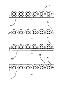
25 to (d) of Figure 2.
Illustration (a) of Figure 2 shows the incorporation of the semiconductor
elements
11 into an insulating support layer 70. Here, it has proven to be advantageous
to
use a flexible film as the support layer. The support layer preferably
consists of a
30 thermoplastic polymer which can be, for instance, a polymer from the
group of the
polycarbonates or polyesters. Pre-polymerized resins from the group of the
epox.
CA 02540723 2006-03-30
WO 2005/034149
PCT/EP2004/010615
14
ides, polyurethanes, polyactylies and/or polyimides can be used. Moreover, a
liq-
uid polymer can be used into which the spheres are pressed and which subse-
quently hardens,
The semiconductor elements 11 are preferably incorporated into the support
layer
70 in such a way that they protrude from the surface of the layer on at least
one
side of the support layer. For this purpose, the particles can be applied, for
exam-
ple, by means of scattering, dusting and/or printing, after which they are
pressed
in. In order to press the bodies into the support layer, the latter can, for
instance,
be heated up.
In another embodiment of the invention, the particles are incorporated into a
pre-
pared matrix of a support layer having recesses into which the particles are
incorporated. In order to attach the bodies to the support layer, a heating
and/or
pressing procedure can be carried out,
If the semiconductor elements are supposed to protrude on both sides of the
sup-
port layer, the support layer can be situated on a flexible base when the
elements
are incorporated, so that the semiconductor elements can be pressed so far
into the
support layer that parts of them emerge from the bottom of the support layer.
In an especially preferred embodiment of the invention, the next step is to
remove
parts of the semiconductor elements on one side of the support layer. Parts of
the
support layer can also be removed in this process. This is shown in the
illustration
(b) of Figure 2 by an arrow. Here, the support layer 70 is preferably removed
down to a layer thickness at which parts of the incorporated bodies are also
removed. In the embodiment shown, the removal extends all the way to the back
contact layer 30 of the semiconductor element 11 as shown by a dotted line. If
the
semiconductor elements are incorporated into the support layer in such a way
that
they protrude from both sides of the layer, it is also possible to process the
semiconductor elements on one side without additional removal of the support
CA 02540723 2006-03-30
WO 2005/034149
PCT/EP2004/010615
layer so that, after the removal procedure, the semiconductor elements either
pro-
trude further from the support layer or are flush with it.
The removal of the semiconductor elements or of the support layer can also be
5 carried out at different points in time before the application of a later
back contact
80 on this side. The removal of the semiconductor elements and/or of the
support
layer can be done by mechanical procedures such as grinding or polishing,
etching,
thermal energy input such as, for instance, using a laser or radiation or else
by
means of photolithographic processes.
In another process step, a conductive back contact layer 80 is applied onto
the side
on which the semiconductor elements had been removed. Examples of conductive
material for this back contact include substances from various classes of
polymers.
Especially well-suited materials are epoxy resins, polyurethanes and/or poly-
imides that have been provided with suitable conductive particles such as
carbon,
indium, nickel, molybdenum, iron, nickel chromium, silver, aluminum and/or the
corresponding alloys or oxides. Another possibility comprises intrinsic
conductive
polymers. These include, for example, polymers from the group of the PANis.
Other materials that can be employed are TCOs or suitable metals, In the case
of
TCOs and metals, the back contact can be applied with PVD or CVD methods.
In another process step, a conductive front contact layer 90 is applied onto
the side
of the support layer on which no semiconductor elements have been removed.
This can also be carried out with methods such as PVD or CVD. Various transpar-
ent conductive oxides (TCOs) can be used as the conductive material of the
front
contact.
Other function layers can be deposited before or after the deposition of a
front
contact and a back contact. The selection of the other function layers depends
especially on the semiconductor elements employed, Function layers such as,
for
example, buffer layers that have already been deposited onto the semiconductor
CA 02540723 2006-03-30
WO 2005/034149 PCT/EP20041010615
16
elements do not necessarily have to be deposited any more for the production
of
the solar cell having integrated semiconductor elements. All of the required
deposition and processing steps yield a solar cell from which a photovoltaic
mod-
ule can be made. One or more of the solar cells can be connected in series,
for
example, and joined to form a module at which the generated current is tapped.
CA 02540723 2006-03-30
WO 2005/034149
PCT/EP2004/010615
17
List of reference numerals
layer structure, precursor layer structure
11 semiconductor element
5 20 substrate, substrate core
30 back contact layer of a semiconductor element
40 rust precursor layer
50 second precursor layer
60 I-III-VI compound semiconductor, CIS or CIGS layer
10 70 support layer, insulating
80 back contact layer of a solar cell
90 front contact layer of a solar cell