Note: Descriptions are shown in the official language in which they were submitted.
CA 02540825 2006-03-30
WO 2005/034170
PCT/EP2004/010781
SERIAL CIRCUIT OF SOLAR CELLS WITH INTEGRATED
SEMICONDUCTOR BODIES, CORRESPONDING METHOD FOR
PRODUCTION AND MODULE WITH SERIAL CONNECTION
Description:
The invention relates to a serial connection of solar cells having integrated
semiconductor elements.
The invention also relates to a method for the production of a serial
connection of
solar cells having integrated semiconductor elements.
The invention also relates to a photovoltaic module with a serial connection
of
solar cells.
In industry, there is an increasing demand for methods for the production of
serial
connections of solar cells. Particularly in the special field of photovoltaics
where
semiconductor particles are incorporated into a layer system in order to form
a p-n
junction, it is practical to combine areas of thin layers and semiconductor
particles
to form cells or arrays and to connect these cells in series so as to be able
to tap
higher voltages. The problem of the serial connection of solar cells having
incorporated semiconductor particles, however, has not yet been satisfactorily
solved.
German patent application DE 100 52 914 Al, for instance, describes a
semiconductor component system in which a semiconductor structure consisting
of layers with incorporated semiconductor particles is completely punctured at
predefined places. insulated conductor pins are inserted into these holes that
have
a size of a few hundred gm and these pins are firmly connected to a conductive
layer on the front. The serial connection of the arrays is achieved by
installing
CA 02540825 2006-03-30
WO 2005/034170 PCT/EP
2004/010781
2
conductor bridges, after which the arrays are electrically separated from each
other at the end of the procedure. The disconnection points are encapsulated
with
insulating and concurrently adhesive materials.
In another embodiment, which is likewise described in German preliminary pub-
lished application DE 100 52 914 Al, the approach taken during the production
of
the semiconductor component system is that different semiconductor component
types (n-material and p-material) are applied alternately onto defined surface
areas.
Thus, areas with positive or negative electrodes are alternately formed on one
side
of a system, and these electrodes can be connected in series by an integrated
connection. For this purpose, the electrode layers are interrupted alternately
on the
top and on the bottom. The placement of different semiconductor component
types in order to create a surface with different electrodes, however, is an
expen-
sive method.
Moreover, U.S. Pat. No. 4,407,320 discloses a method for the production of
solar
cells in which spherical semiconductor elements are incorporated into an
insulat-
ing layer. The spheres have a semiconductor of n-type material on one side
whereas they have a semiconductor of p-type material on the other side. In
each
case, a conductive layer is applied onto both sides of the insulating layer in
order
to connect the spheres to each other. Furthermore, conductive separation lines
are
made consisting of spheres, a paste or, for example, a wire. In order to
produce a
serial connection, alternating cuts are made into the conductive layers on
both
sides of the conductive separation line.
It is also a known procedure to configure independent spherical semiconductor
elements that constitute complete semiconductors, including the requisite elec
AMENDED PAGE
CA 02540825 2011-11-03
- 2a -
trodes. For example, European patent application EP 0 940 860 Al describes
using a spherical core to make a spherical semiconductor element by means of
masking, etching steps and the application of various material layers. Such
semiconductor elements can be used as solar cells if the p-n junction is
selected in
such a way that it can convert incident light into energy. If the p-n junction
is
configured in such a way that it can convert an applied voltage into light,
then the
semiconductor element can be employed as a light-emitting element.
Moreover, U.S. Pat. No. 5,578,503 discloses a method for the rapid production
of
chalcopyrite semiconductor layers on a substrate in which individual layers of
the
elements copper, indium or gallium and sulfur or selenium are applied onto a
substrate in elemental form or as a binary interelemental compound. The
substrate
with the layer structure is then quickly heated up and kept at a temperature
of
350 C [?_ 662 F] for between 10 seconds and one hour.
The invention provides a method for the production of serial connections of
solar
cells having integrated semiconductor elements that can be carried out with
just a
few simple process steps.
Moreover, the invention provides a serial connection of solar cells having
integrated semiconductor elements that is produced with just a few process
steps
that are simple to carry out.
Furthermore, the invention provides a photovoltaic module with serially
connected solar cells.
According to an aspect of the invention, there is provided a method for the
production of a serial connection of solar cells having integrated
semiconductor
elements, characterized by the following features: incorporation of one or
more
conductive elements into an insulating support layer according to a pattern,
CA 02540825 2011-11-03
- 2b -
whereby the conductive elements protrude from the surface of the support layer
on
at least one side of the support layer, and the pattern calls for at least one
separation line having a width B and consisting of one or more conductive
elements; incorporation of several spherical or grain-shaped semiconductor
elements into the insulating support layer according to a pattern, whereby the
semiconductor elements consist of substrate cores that are coated at least
with one
conductive back contact layer made of molybdenum and with one semiconductor
layer made of a I-111-VI compound semiconductor arranged above it, the
semiconductor elements protrude from the surface of the support layer on at
least
one side of the support layer, and the pattern provides that the areas next to
a
separation line or between several separation lines consisting of conductive
elements are fitted with semiconductor elements; removal of parts of the
semiconductor elements on one side of the support layer until the back contact
layer of the semiconductor elements is exposed; application of a conductive
back
contact layer onto the side of the support layer on which parts of the
semiconductor elements have been removed; application of a conductive front
contact layer onto the side of the support layer on which no semiconductor
elements have been removed, whereby before and/or after the deposition of the
front contact layer and/or of the back contact layer, a buffer layer made of
CdS
and/or a layer made of intrinsic zinc oxide are deposited, or a buffer layer
made of
CdS and/or a layer made of intrinsic zinc oxide had already been deposited
onto
the spherical or grain-shaped semiconductor elements employed; making of two
separation cuts along a separation line consisting of conductive elements,
whereby
a first separation cut is made in the front contact layer and a second
separation cut
is made in the back contact layer, the separation cuts are on different sides
of the
appertaining separation line, and the separation cuts penetrate the back
contact
layer all the way to the support layer.
According to another aspect of the invention, there is provided a serial
connection
of solar cells having integrated semiconductor elements, characterized in that
the
CA 02540825 2011-11-03
- 2c -
serial connection has at least the following features: an insulating support
layer into which one
or more conductive elements are incorporated according to a pattern, whereby
the conductive
elements protrude from the surface of the support layer on at least one side
of the support layer,
and the pattern calls for at least one separation line having a width B and
consisting of one or
more conductive elements; several spherical or grain-shaped semiconductor
elements in the
insulating support layer, whereby the semiconductor elements consist of a
substrate core that is
coated at least with one conductive back contact layer made of molybdenum and
with one
semiconductor layer made of a compound semiconductor, and the
semiconductor
elements protrude from the surface of the support layer on at least one side
of the support layer
and form a pattern in which the areas next to a separation line or between
several separation
lines are fitted with semiconductor elements; a conductive front contact layer
on one side of
the support layer on which the elements protrude from the layer; a conductive
back contact
layer on the side of the support layer that is opposite from the front contact
layer; a buffer layer
made of CdS and/or a layer made of intrinsic zinc oxide, or a buffer layer
made of CdS and/or
a layer made of intrinsic zinc oxide already on the spherical or grain-shaped
semiconductor
elements employed; in each case, two separation cuts along a row of conductor
elements,
whereby a first separation cut is made in the front contact layer and a second
separation cut is
made in the back contact layer, the separation cuts are on different sides of
the appertaining
row of conductive elements, and the separation cuts penetrate the back contact
layer all the
way to the support layer; and on the side of the support layer on which the
back contact layer
of the solar cell is arranged, at least one of the semiconductor elements has
a surface via which
a direct contact is established between the back contact layer of the solar
cell and the back
contact layer of the semiconductor element.
According to another aspect of the invention, there is provided a photovoltaic
module,
characterized in that it comprises a serial connection as described above.
CA 02540825 2006-03-30
WO 2005/034170
pCT/EP2004/010781
3
In the method according to the invention for the production of a serial
connection
of solar cells having integrated semiconductor elements, one or more
conductive
elements and spherical or grain-shaped semiconductor elements are incorporated
into an insulating support layer according to a pattern, whereby the elements
pro-
trude from the surface of the support layer on at least one side of the
support layer,
and the pattern calls for at least one continuous separation line having a
width B
consisting of conductive elements, The areas next to a separation line or
between
several lines are fitted with semiconductor elements.
In an especially preferred embodiment of the invention, the pattern in the
support
layer provides that a distance exists between a separation line and an area
that is
fitted with semiconductor elements, so that, next to a separation line, a thin
strip is
formed into which separation cuts can be made without the conductive elements
or the semiconductor elements being touched and likewise being cut. It is also
possible not to have any distance so that the separation cuts are made in such
a
way that, as a result, parts of the conductive elements and/or of the
semiconductor
elements are cut off.
The elements incorporated into the support layer can be, for example, elements
made of solid material or else coated substrate cores. Examples of conductive
ele-
ments can be, for example, particles made of a conductive material or
particles
coated with a conductive material. In a preferred embodiment of the invention,
the
conductive material is copper. In another especially preferred embodiment of
the
invention, particles made from 1-111-1/1 compound semiconductors or substrates
coated with I-III-VI compound semiconductors are used as the semiconductor ele-
ments, so that the designation "semiconductor element" can refer to any
element
in which one constituent is a semiconductor material.
In another embodiment of the invention, the conductive elements are formed by
one or more strips, This has the advantage that a continuous separation line
can be
created. Furthermore, it has proven to be advantageous to incorporate a conduc-
CA 02540825 2006-03-30
WO 2005/034170
PCT/EP2004/010781
4
live element in the form of a paste into the support layer. This is especially
advantageous when the support layer is a matrix with recesses for elements
that
are to be incorporated. Thus, the conductive paste can be applied onto one
side of
the matrix and can be pressed through the recesses to the other side of the
matrix
so that both sides have conductive separation lines that are contacted all the
way
through the support layer.
According to the invention, parts of the semiconductor elements are removed
from one side of the support layer. This is done in order to expose a surface
area
of the semiconductor element that is to be contacted with the back contact of
the
solar cell. This is preferably a back contact layer that was deposited onto
the
semiconductor element below a semiconductor layer so that removal of the
semiconductor layer is necessary. Furthermore, a back contact layer is applied
onto the side of the support layer on which the semiconductor elements have
been
removed and a front contact layer is applied onto the other side of the
support
layer. The front contact layer and the back contact layer consist of a
conductive
material.
In order to produce a solar cell, depending on the envisaged embodiment, other
function layers can be applied, which can include, for example, a buffer layer
made of CdS, intrinsic zinc oxide and/or a transparent conductive oxide (TCO)
layer. In another especially preferred embodiment of the invention, in
addition to
a back contact layer and a semiconductor layer, the semiconductor elements com-
prise other function layers, which can likewise include a buffer layer made of
CdS,
intrinsic zinc oxide and/or a TCO layer.
In another process step, two separation cuts are made along a row of
conductive
elements, whereby a first separation cut is made in the front contact layer
and a
second separation cut is made in the back contact layer. Here, the separation
cuts
are on different sides of the appertaining separation line consisting of
conductive
elements, and they penetrate the back contact layer all the way to the support
layer.
CA 02540825 2006-03-30
WO 2005/034170
PCT/EP2004/010781
In an especially preferred embodiment of the invention, the row of conductive
ele-
ments is essentially straight and extends between two edges of the support
layer
that are opposite from each other. However, the pattern of separation lines
consist-
5 ing of conductive elements and areas between them in the form of solar
cells can
be selected freely so that, for instance, curved separation lines are also
possible.
The conductor elements and semiconductor elements can be, for example, scat-
tered on and then pressed in. In an especially preferred embodiment of the
inven-
tion, the spherical or grain-shaped elements are incorporated into a matrix of
a
support layer having prepared recesses for the elements. The elements can be
incorporated into the support layer, for example, by means of a heating and/or
pressing procedure. Various physical vapor deposition (PVD) and/or chemical
vapor deposition (CVD) methods or other methods that have been adapted to the
type of the layer in question can be used in order to apply the front contact
layer
and the back contact layer. If, for example, a conductive adhesive is used,
brush-
ing on or spreading on the adhesive has proven to be advantageous.
The method according to the invention makes it possible to generate a serial
connection in which the current flows through an area of semiconductor
elements
of the front contact layer into the separation line consisting of conductive
ele-
men. The further flow of the current out of the conductor elements into the
next
area of semiconductor elements of the front contact layer, however, is
prevented
by a first separation cut so that the current flows via the conductive
elements into
the back contact. Here, the current flow through the back contact is prevented
by a
second separation cut in the back contact. Thus, between the separation lines
consisting of conductive elements, areas are formed that function as solar
cells
and that are connected in series with each other.
For this purpose, the serial connection of solar cells having integrated
semiconductor elements has at least one insulating support layer in which
conduc-
CA 02540825 2006-03-30
W02805/034110
PCIMP2004/010781
6
tive elements and spherical or grain-shaped semiconductor elements are incorpo-
rated according to a pattern, whereby the elements protrude from the layer on
at
least one side of the support layer. The pattern calls for least one
continuous
separation line having a width B consisting of conductive elements, whereas
the
areas next to a row or between several rows are fitted with semiconductor ele-
ments.
The serial connection also has a front contact layer and a back contact layer,
whereby the back contact layer lies on the side of the support layer on which
parts
of the semiconductor elements have been removed. In each case, two separation
cuts are made along a separation line consisting of conductive elements,
whereby
a first separation cut is made in the front contact layer and a second
separation cut
is made in the back contact layer. The separation cuts are on different sides
of
each row of conductive elements, and they penetrate the back contact layer all
the
way to the support layer.
When the serial connection is produced with the method according to the inven-
tion, on the side of the support layer on which the back contact layer of the
solar
cell is arranged, at least one of the spherical or grain-shaped semiconductor
ele-
mania has a surface via which a direct contact is established between the back
contact layer of the solar cell and a back contact layer of the semiconductor
ele-
ment. If the semiconductor elements are, for example, a substrate coated with
a
back contact and with a semiconductor, then the coating is removed from the
semiconductor elements to such an extent as to form a surface consisting of
back
contact that can be contacted with the back contact layer of the solar cell.
If, in
addition to a back contact layer and a semiconductor layer, the semiconductor
ele-
ments have other function layers, then these were likewise removed so as to
expose a surface consisting of the back contact.
The essential advantage of the serial connection according to the invention of
solar cells and of the appertaining method for its production lies in the
simple
CA 02540825 2006-03-30
WO 2005/034170
PCT/EP2004/010701
7
configuration of the connection of the solar cell areas, which calls for only
a few
processing steps. The requisite conductive elements can be incorporated in
various
forms and in different ways and the creation of the separation cuts is
likewise a
simple process step.
If spherical or grain-shaped elements are used, these can be incorporated with
the
same method as the semiconductor elements so that no additional methods or
devices have to be developed and implemented for this purpose. If, for
example, a
paste that is applied onto a support matrix having recesses is used as the
conduc-
tive element, then two separation lines that are joined via the support layer
can be
created in a simple manner. Moreover, the additional material requirements are
low since only conductive elements have to be incorporated. The separation
cuts
that are made do not interfere with the overall arrangement since the
weakening of
the overall structure is very slight.
Further advantages, special features and practical embodiments of the
invention
can be gleaned from the subordinate claims and from the presentation below of
preferred embodiments making reference to the figures.
The figures show the following:
Figure 1 in illustrations (a) to (c), the embedding of spherical semiconductor
and conductor particles into a support layer;
Figure 2 in illustrations (a) to (c), the structure of front contact layers
and back
contact layers;
Figure 3 in illustrations (a) to (b), the serial connection according to the
inven-
tion of solar cells having integrated semiconductor particles; and
CA 02540825 2006-03-30
WO 2005/034170
PCT/EP2004/010701
8
Figure 4 an especially preferred embodiment of a shingle-like connection of
several serial connections.
Illustrations (a) to (c) of Figure 1 show the incorporation of spherical or
grain-
shaped conductive elements 20 and semiconductor elements 30 into an insulating
support layer 10. It has proven to be advantageous here to use a flexible film
as
the support layer. The support layer preferably consists of a thermoplastic
material
into which the conductive elements can be pressed. Polymer has proven to be
especially practical and it can be, for example, a polymer from the group
compris-
ing epoxides, polycarbonates, polyesters, polyurethanes, polyacrylics and/or
poly-
imides.
The embedded elements are preferably spherical or grain-shaped particles with
conductive or semiconductive properties. In addition to the pure spherical
shape,
the elements can also have irregular shapes like those of grains having any
con-
tour. These also include, for example, cubes, parallelepipeds or pyramids.
There-
fore, spheres or grains made of conductive materials such as copper can be
used as
the conductive elements 20. in another especially preferred embodiment of the
invention, the conductive elements are incorporated in the form of strips or a
paste
in the shape of a separation line.
The semiconductor elements consist completely or partially of suitable
semiconductor materials used in photovoltaics. in an especially preferred
embodi-
ment of the invention, the semiconductor materials come from the class of the
compound semiconductors, including for instance, copper indium di-
selenide, copper indium disulfide, copper indium gallium diselenide or copper
indium gallium diselenide disulfide. In another embodiment of the invention,
the
semiconductor elements consist of silicon semiconductors. These can be
semiconductors made of solid material or substrate cores coated with
semiconduc-
tor materials,
CA 02540825 2006-03-30
WO 2005/034170
PCT/EP2004/010781
9
The conductive elements and the semiconductor elements are incorporated into
the support layer 10 in such a way that they protrude from the surface of the
layer
on at least one side of the support layer. For this purpose, the elements can
be
applied, for example, by means of scattering, dusting and/or printing, after
which
they can be pressed in. In order to press the elements into the support layer,
it can,
for instance, be heated up. The elements can be arranged into a desired
pattern, for
example, using an auxiliary means, and in this manner, placed onto or into the
support layer.
In an especially preferred embodiment of the invention, the elements are
incorpo-
rated into a prepared matrix of a support layer in which there are recesses
into
which the appertaining elements are inserted. In order to attach the elements
to the
support layer, a heating and/or pressing procedure can be carried out, For
example,
if a paste is used as the conductive element, the paste can be applied onto
desired
areas of the matrix and pressed into the recesses located there. The paste can
be
spread on the back of the support layer so that a separation line is formed on
both
sides of the insulating support layer which are connected to each other by the
recesses.
The conductive elements are incorporated into the support layer according to a
pattern that calls for at least one essentially straight separation line
having a cer-
tain width 8 consisting of conductive elements 20. In this context, the fact
that the
row is essentially straight means that slight deviations from a straight line
are also
comprised. If a geometrically different delineation between individual solar
cells
is to be made for certain applications, a different course of the rows of
conductive
elements can be selected such as, for example, curved separation lines.
Preferably, the separation line consisting of conductive elements extends
between
two edges of the support layer 10 that are opposite from each other. The width
of
the rows of conductive elements is preferably in the order of magnitude of B
10 gm to 3 mm and, depending on the dimensions of the conductive elements
CA 02540825 2006-03-30
WO 2005/034170
PCT/EP20041010781
employed, is defined by one or more conductive elements. In an especially pre-
ferred embodiment of the invention, the width of the separation lines is
between
10 gm and 30 gm. If spherical or grain-shaped particles are used as the
conductive
elements, the width of the separation lines is a function of the diameter of
the
5 particles employed. Consequently, the width of the separation lines can
also be in
the order of magnitude of one or more diameters of a conductive sphere, espe-
cially between 10 gm and 500 gm.
Depending on the desired width of a solar cell that is to be connected, a
support
10 layer is divided into appropriate areas by several rows of conductive
elements.
The areas next to a separation line or between several separation lines are
fitted
with semiconductor elements. The width of a solar cell thus limited is
preferably
in the order of magnitude of 1 mm to 3 cm. In an especially preferred
embodiment
of the invention, the width of a solar cell is between 3 mm and 5 mm. The
width
of a support layer with a serial connection thus formed is preferably in the
order of
magnitude of 5 cm to 30 cm, whereby it has proven to be especially
advantageous
to have strip-like modules consisting of several serially connected solar
cells that
preferably have a width of approximately 10 cm.
The illustrations (a) to (c) of Figure 2 show the formation of the layer
structure for
the production of a solar cell having integrated semiconductor elements. In an
especially preferred embodiment of the invention, as a first step, material is
removed from one side of the support layer 10. This side is removed down to a
layer thickness at which parts of the incorporated elements have likewise been
removed. The areas of the elements that have likewise been removed are shown
in
illustration (a) by the remaining contours of two conductive and semiconductor
elements shown by a broken line. The removal of the support layer, however,
can
also take place at other points in time that precede the application of a
later back
contact 50 on this side.
CA 02540825 2006-03-30
WO 2005/034170
PCTJEP2004/010781
11
In another embodiment of the invention, after the incorporation, the
semiconduc-
tor elements protrude from one side of the support layer to such an extent
that
parts of them can be removed without a simultaneous removal of the support
layer
being necessary. The conductive elements, the semiconductor elements and/or
the
support layer can be removed, for example, by mechanical methods such as grind-
ing, polishing, chemical or wet-chemical methods (processes) such as etching,
photolithography or thermal energy input, for instance, by means of lasers or
radiation with light having a suitable wavelength or wavelength range or by
other
thermal methods.
The extent of the removal depends primarily on the semiconductor elements
employed. If, for example, spherical or grain-shaped substrate cores are used,
which are coated at least with one back contact layer and with one
semiconductor
layer, the removal is carried out until the back contact layer of the particle
is
exposed in order to establish the contact with the back contact of the solar
cell. In
an especially preferred embodiment of the invention, the semiconductor
elements
are glass substrate cores that are coated with a back contact made of
molybdenum
and with a semiconductor. In this case, the removal of the support layer is
carried
out down to a layer thickness in which the molybdenum layer of the elements is
exposcd.
In this context, the removal also depends on whether all of the semiconductor
ele-
ments are situated at equal depths in the support layer. If the semiconductor
ele-
ments are embedded at different depths or if the size of the elements varies,
then
the possibility exists that not all of the semiconductor elements will have
their
coating removed down to their back contact layer.
In another process step, a back contact layer 50 is applied onto the side of
the sup-
port layer 10 on which at least parts of the semiconductor elements have been
removed. Conductive substances such as metals are used as the material for
this
back contact. It is also possible to use transparent conductive oxides (TC0s)
or
CA 02540825 2006-03-30
WO 20051034170
PCT/EP2004/010781
12
substances from various polymer classes. Especially suitable materials are,
for
example, epoxy resins, polyurethanes and/or polyimides that have been provided
with suitable conductive particles such as carbon, indium, nickel, molybdenum,
iron, nickel chromium, silver, aluminum and/or the corresponding alloys or
oxides.
Another possibility comprises intrinsic conductive polymers. These include,
for
example, polymers from the group of the PAN is. The back contact can be pro-
duced by means of PVD methods such as sputtering and evaporation coating or
CVD methods such as PE-CVD or MO-PVD or else with another technique that is
adapted to the back contact material.
In another process step, a conductive front contact layer 40 is deposited onto
the
side of the support layer on which no processing of the elements was carried
out.
This can also be done with PVD or CVD methods as well as other methods that
are adapted to the front contact material. Various transparent conductive
oxides
(TC0s) such as, for instance, aluminum-doped zinc oxide (ZnO:AI) (also called
AZO), indium tin oxide (ITO) or fluorine-doped tin oxide (Sn02:F) can be used
as
the material for the front contact. It has proven to be advantageous to use a
transparent front contact whose transmission is preferably adapted to the
semiconductor in question.
Other function layers can be deposited before and/or after the deposition of a
front
contact and/or a back contact. These include, for example, a buffer layer made
of
CdS, intrinsic zinc oxide and/or another TCO layer. In an especially preferred
embodiment of the invention, these function layers have already been deposited
onto the semiconductor elements employed so that there might not be a need for
another deposition procedure in order to produce a solar cell.
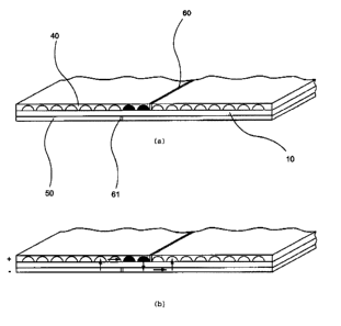
As another essential process step, two separation cuts 60 and 61 are made
along a
row of conductive elements as is shown in illustration (a) of Figure 3. Here,
a
separation cut 60 is made into the front contact layer 40 and a separation cut
61 is
made into the back contact layer, whereby said separation cuts lie on
different
CA 02540825 2006-03-30
WO 2005/034170
PCT/EP20041010781
13
sides of the row of conductive elements 20. The separation cuts can be made
using
methods such as cutting, scoring, thermal energy input such as, for example,
laser
cutting or else by means of photolithographic processes.
=
In an especially preferred embodiment of the invention, the separation cuts
thus
created are filled up with an insulating material in order to achieve the
flattest
possible surface of the solar cell connection. However, this step is optional
since
the requisite depth of the separation cuts 60; 61 is very small due to the
fact that
the thin front contact and back contact layers are in the um range.
Once the procedure has been completed and all deposition and separation steps
have been carried out, the resulting layers with the semiconductor elements
constitute a serial connection of solar cells that can be used in a
photovoltaic mod-
ule. Depending on the embodiment of the photovoltaic module, it can comprise
one or more serial connections, The resultant current course is indicated in
illustration (b) of Figure 3 by several arrows, in the embodiment shown, the
nega-
tive front contact is on the top whereas the positive back contact is on the
bottom.
The current flows via the semiconductor element 30 in the front contact into
the
conductive element 20 and from there into the back contact 50, since a
fiirther cur-
rent flow is prevented by the first separation cut 60. The current flow
through the
back contact 50 is prevented by the second separation cut 61.
In an especially preferred embodiment of the invention, such a serial
connection is
joined to at least one other corresponding serial connection so as to form a
larger
module. This is done, for example, in that the individual serial connections
are
configured so as to be strip-like with a width in the order of magnitude of 5
cm to
cm and the sub-modules thus formed are laid over each other at the edges like
shingles. This is shown in Figure 4. Hence, a back contact comes to lie on a
front
contact and the individual modules are, in turn, connected in series. The
contact-
30 ing between each front contact layer and back contact layer can be done
by means
of a conductive adhesive such as silver epoxide.
CA 02540825 2006-03-30
WO 2005/034170
PCT/EP2004/010781
14
List of reference numerals
support layer, film
conductive element, conductor element
5 21 separation line
semiconductor element, spherical or grain-shaped
front contact layer
back contact layer
60, 61 separation cuts