Note: Descriptions are shown in the official language in which they were submitted.
CA 02540941 2006-03-30
WO 2005/043624
PCT/US2003/031337
FABRICATION OF THERMAL DETECTING STRUCTURES
Background of the Invention
The present invention relates generally to the fabrication of thermal, e.g.,
infrared (IR), detecting structures. More particularly, the present invention
pertains to the fabrication of electrical connections associated with thermal
detecting structures.
A thermal detecting structure can be generally defined as a very sensitive
thermometer that is used in the detection and measurement of thermal
radiation.
For example, a thermal detecting structure may be used to detect IR radiation,
and therefore, operate as an IR sensor. Fabrication of a thermal detecting
structure generally includes providing a thermal detecting material.
The thermal detecting material desirably includes a measurable property
that varies with detected thermal radiation. For example, the resistance of
the
material may vary as a function of detected thermal radiation. A goal in the
design of thermal detecting structures is to maximize the sensitivity of the
thermal measurements. One factor in the sensitivity of resistance-based
thermal
detecting structures is a property of the thermal detecting material called
thermal
coefficient of resistance (TCR) (often expressed in % change in resistance per
C). For example, the thermal detecting material may be selected to provide the
highest TCR that is compatible with the other materials and processes used in
the fabrication of the thermal detecting structures.
One example of a thermal detecting structure is a two-level infrared
thermal detecting array as described in U.S. Patent No. Re. 36,136, entitled
"Thermal Sensor," issued to Higashi et al. on 9 March 1999. This thermal
detecting structure includes a detector structure with integrated circuitry on
a
silicon substrate beneath the detector structure. The use of the two-level
structure may, for example, provide the ability to form more detectors in a
particular area.
1
CA 02540941 2006-03-30
WO 2005/043624
PCT/US2003/031337
Another example of a previous theimal detecting structure is a two-level
infrared thermal detecting array as described in U.S. Patent No. 6,144,285,
entitled "Thermal Sensor and Method of Making Same," issued to Higashi on 7
November 2000. This thermal detecting structure includes an upper detector
section that includes a temperature responsive detector of a vanadium oxide
having a high TCR above a lower section that includes integrated circuits. The
upper detector section is supported above the lower section by leg portions of
the vanadium oxide. The leg portions may be electrically connected both to the
detector of the upper section and to the integrated circuits of the lower
section.
In other words, the vanadium oxide used to form the detector also provides
electrical connection therefrom to the integrated circuits of the lower
section
eliminating the need for using other interconnect materials to make such
connections. As described therein, a back sputtering process is used to reduce
the sheet resistance of the vanadium oxide that forms the interconnects.
A goal in the design of the electrical connections between the thermal
detector and integrated circuitry of the thermal detecting structures below
the
detector is to lower the electrical resistance of such connections.
Summary of the Invention
The methods described herein enhance the performance of thermal
detecting structures. For example, such processes reduce the resistance of one
or more electrical connections. Reducing the resistance of the electrical
interconnects provides a reduction in the electrical noise levels which
enhances
the performance of the thermal detecting structure. For example, lower
resistance reduces noise which improves the signal to noise ratio and
therefore
improves the sensitivity of the thermal detecting structure.
The present method exploits the use of a process to reduce the resistance
of thermal detecting material such that a low resistance contact may be formed
between the thermal detecting material and a conductive material. Thus, a
conductive material may be utilized to form a low-resistance connection
between the thermal detecting material and other conductive contacts.
2
CA 02540941 2006-03-30
WO 2005/043624
PCT/US2003/031337
The method of fabricating a thermal detecting structure according to the
present invention includes providing a substrate assembly including conductive
contacts, and founing a thermal detecting material on at least a portion of
the
substrate assembly. A contact region including an exposed surface of the
thermal detecting material is defined. The exposed surface of the thermal
detecting material is subjected to contact with inert gas ions to alter the
exposed
surface. Conductive material is provided in contact with at least the altered
exposed surface of the thermal detecting material for use in forming an
electrical connection to at least one conductive contact.
In one embodiment, the contact region is defined by forming at least one
insulating layer on a least a portion of the thermal detecting material. One
or
more portions of the at least one insulating layer may be removed for use in
defining the contact region including the exposed surface of the thermal
detecting material, and further, for use in exposing at least one conductive
contact of the substrate assembly.
In one embodiment of the method, subjecting at least the exposed
surface of the thermal detecting material includes back sputtering at least
the
exposed surface of thermal detecting material.
In another embodiment of the method, back sputtering at least the
exposed surface of the thermal detecting material includes providing a chamber
in which the substrate assembly having the thermal detecting material formed
thereon may be positioned and subjecting at least the exposed surface of
thermal
detecting material to contact with inert gas ions. For example, subjecting the
exposed surface to contact with inert gas ions may include biasing the
substrate
assembly.
In another embodiment of the method, the thermal detecting material
includes a metal component and a non-metal component. The non-metal
component of the thermal detecting material may be removed faster than the
metal component when subjected to contact with inert gas ions.
In yet another embodiment of the method, the thermal detecting material
includes vanadium oxide (V0x); x may be in the range of about 1.0 to about
2.5.
3
CA 02540941 2006-03-30
WO 2005/043624
PCT/US2003/031337
Yet further, according to another embodiment of the present method, the
thermal detecting structure may include a detector assembly spaced from a
portion of the substrate assembly by a gap.
In other embodiments of the present method, forming the electrical
connection to the at least one conductive contact may include providing a via
(e.g., the via may include providing a basket-shaped via or a post-shaped via)
and the conductive material used to make the electrical connection may include
at least one of nickel and chromium.
The above summary of the present invention is not intended to describe
each embodiment or every implementation of the present invention.
Advantages, together with a more complete understanding of the invention, will
become apparent and appreciated by referring to the following detailed
description and claims taken in conjunction with the accompanying drawings.
Brief Description of the Drawings
Figure 1 is a schematic diagram of one embodiment of a thermal
detecting structure fabricated using a fabrication process according to the
present invention.
Figure 2 is one embodiment of a general flow diagram of a fabrication
process according to the present invention.
Figure 3 is a perspective view of one embodiment of a thermal detecting
structure fabricated using a process such as that shown in Figure 6.
Figure 4 is a cross section of Figure 3 taken along Line 4-4, showing the
thermal detecting material including the contact regions.
Figure 5 is a cross section of Figure 3 taken along Line 5-5, showing a
portion of the electrical connection including a basket-shaped via.
Figure 6 is one embodiment of the general flow diagram of Figure 2
showing a fabrication process according to the present invention.
Figures 7A-7E illustrate cross-section views of a thermal detecting
structure (e.g., such as that shown in Figure 3) during a fabrication process
for
forming such a structure such as the fabrication process as shown in Figure 6.
4
CA 02540941 2006-03-30
WO 2005/043624
PCT/US2003/031337
Detailed Description of the Embodiments
The method of the present invention shall be described generally with
reference to Figures 1-2. Thereafter, various other embodiments of the present
invention shall be described with reference to Figures 3-7. The present
invention provides low resistance connections associated with thermal
detecting
structures. It should be apparent that the scaling in the figures does not
represent precise dimensions of the various elements illustrated therein.
In this application, substrate assembly refers to an assembly upon which
additional layers and structures may be fabricated. When reference is made to
a
substrate assembly in the following description, various process steps may
have
been previously utilized to form layers, vias, or other structures as known to
one
skilled in the art.
In this application, via refers to an opening to which conductive material
may be added to form a conductive path through the opening, such that the via
can be used to form an electrical connection.
Figure 1 illustrates one general embodiment of a thermal detecting
structure 100 that may be fabricated using a method according to the present
invention such as generally shown in the embodiment of Figure 2. The thermal
detecting structure 100 includes a detector assembly 102 and a substrate
assembly 116. The detector assembly 102 includes a thermal detecting material
104 that may be formed relative to the substrate assembly 116. The thermal
detecting material 104 includes a temperature responsive detector region 106
and contact regions 108, 110. The substrate assembly 116 includes conductive
contacts 118, 120.
Two electrical connections 111, 113 may be formed to electrically
connect the thermal detecting material 104 to the conductive contacts 118,
120.
Connection 111 may be formed to electrically connect contact region 108 to
conductive contact 118 and connection 113 may be formed to electrically
connect contact region 110 to conductive contact 120. The connections between
the temperature responsive detector region 106 (e.g., thermal detecting
material)
and conductive contacts 118, 120 may be provided using any number of
structures including, but clearly not limited to: portions of the temperature
CA 02540941 2006-03-30
WO 2005/043624
PCT/US2003/031337
responsive detector region 106; the contact region 108, 110; the conductive
material 112, 114; and the conductive contact 118, 120. Other structures that
may be used to form the electrical connection include, for example, structures
such as vias, basket-shaped vias (see Figure 3, 326, 328), post-shaped vias,
openings lined with conductive material, thermal detecting material, or
suspended conductive material. For example, structures described in U.S.
Patent No. Re. 36,136, Higashi et all. may be used (e.g., a two-level thermal
detecting structure in which the connections from the thermal detecting
material
to the conductive contacts are formed using conductive material).
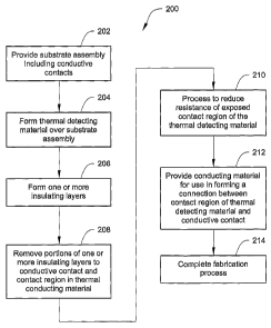
Figure 2 illustrates one general embodiment of a process flow 200 that
may be used to provide a thermal detecting structure such as that shown in
Figure 1. However, one skilled in the art will recognize that other thermal
detecting structures may be formed thereby. In one or more embodiments, the
process flow 200 may be used to fabricate a single thermal detecting
structure,
or the same process can be used to fabricate multiple thermal detecting
structures simultaneously (e.g., fabricate an array of thermal detecting
structures
on a wafer).
The process flow 200 shown in Figure 2 begins with provision of a
substrate assembly 116 (block 202). The fabrication of the substrate assembly
116 may be performed using various techniques known to those skilled in the
art. As described previously, a substrate assembly may include a substrate
upon
which various features and devices using, for example, various layers and
structures, may be fabricated. The substrate assembly 116 includes conductive
contacts 118, 120. The substrate assembly may include additional structures
and devices. For example, the devices and structures that may be formed
include, but are not limited to: bipolar transistors; field effect transistors
(FET);
diodes; pads; lines; planarization layers; sacrificial layers; reflective
layers,
insulating layers formed from various materials; conductive interconnects;
vias;
or any integrated circuit structures, any devices, or any other structures
known to
one skilled in the art. The substrate assembly may be formed from a variety of
materials. The substrate may be any structure that is a suitable underlying
structure for the method of the present invention. For example, a substrate
6
CA 02540941 2006-03-30
WO 2005/043624
PCT/US2003/031337
assembly of a thermal detecting structure is described in U.S. Patent No. Re.
36,136 to Higashi et al.
As further shown in Figure 2, a thermal detecting material 104 may be
formed over at least a portion of the substrate assembly 116 (block 204). For
example, the thermal detecting material may be deposited over the entire
surface
and then patterned to form the detector region 106. Formation of such material
may be accomplished with any process compatible with the selected thermal
detecting material.
The thermal detecting material may be any material that provides the
desired thermal characteristics and is compatible with the processes and other
materials used. For example, materials that may be used as thermal detecting
material include vanadium oxide (VOx), InSb (a semiconductor), FeO (a metal
oxide), or NbV0 (a metal oxide).
In one embodiment of the present invention, preferably VOx is used as
the thermal detecting material. VOx may be characterized by having a high
temperature coefficient of resistance (TCR) in the range of about 0.5 %/ C to
about 5 %/ C. U.S. Patent No. 6,322,670 entitled "Flexible High Performance
Microbolometer Detector Material Fabricated Via Controlled Ion Beam Sputter
Deposition Process," issued to Cole et al. on 27 November 2001, and U.S.
Patent No. 6,495,070, entitled "Flexible High Performance Microbolometer
Detector Material Fabricated Via Controlled Ion Beam. Sputter Deposition
Process," issued to Cole et al. On 17 December 2002, describe the use of VOx
material and a method for providing and using VOx material in a fabrication
process.
In one embodiment, various layers may be formed prior to forming the
thermal detecting layer 104. For example, as shown in Figures 7A and 7B, prior
to forming the thermal detecting material 304, a substrate assembly 316 may be
formed including an integrated circuit 338 including conductive contacts 318,
320. A planarization layer 340 may be formed over integrated circuit 338. A
sacrificial layer 348 may be formed over the planarization layer 340 and an
insulating layer 346 may be formed over the sacrificial layer 348. The thermal
detecting material 304 may be then formed over insulating layer 346.
7
CA 02540941 2006-03-30
WO 2005/043624
PCT/US2003/031337
Figure 2 further shows forming one or more insulating layers relative to
the thermal detecting material (block 206). Such insulating layers may be used
during the fabrication process (e.g., insulating layers 334, 336 such as
described
with respect to the process flow shown in Figures 7B to 7E), and may or may
not be present when the fabrication is complete, thus they are not shown in
Figure 1. These layers may be used during fabrication, for example, to provide
protection for underlying layers or to provide a mask layer for subsequent
process steps. In one embodiment of the present invention, there may be at
least
one insulating layer on the thennal detecting material to provide a mask for
use
in subsequent process steps. These insulating layers may be formed from a
variety of materials and the number of insulating layers may vary.
Various insulating layer materials may be selected for use in the method
of the present invention. Generally, such materials are compatible with other
process materials and processes used in the fabrication of the thermal
detecting
structures. For example, such materials may provide one or more of the
following functions: mechanical support; patternability; thermal isolation;
and
electrical isolation. For example, silicon dioxide, silicon oxynitride, or
silicon
nitride may be used to form insulating layers. These materials provide thermal
isolation, electrical isolation, and are generally patternable.
At least portions of the one or more insulating layers may be removed to
form openings to conductive contacts 118, 120 (block 208). In addition,
portions of the same insulating layers or different insulating layers may be
removed to form the contact regions 108, 110 of the thermal detecting material
104. In other words, the insulating layers may be patterned to provide
openings
for subsequent process steps.
For example, in one embodiment such as shown in Figures 7B and 7C,
one or more insulating layers 334, 336 may be patterned such that material may
be selectively removed (e.g., by etching) in subsequent steps. Figure 7C shows
openings 362, 364 created such that in a subsequent step, conductive material
may be formed to provide a connection to the conductive contacts 318, 320.
Openings 362, 364 may be created by removing insulating layer 336 from the
8
CA 02540941 2006-03-30
WO 2005/043624
PCT/US2003/031337
basket-shaped opening 342, 344 and further, removing a portion 384, 386 of the
planarization layer 340, thus exposing conductive contacts 318, 320.
Further, for example, Figure 7C shows openings 366, 368 created such
that in a subsequent step, conductive material may be formed to provide a
connection to the contact regions 308, 310 of the thermal conducting material
304. Openings 366, 368 may be created by removing one or more insulating
layers 334, 336 from the contact region 308, 310 of the thermal conducting
material 304 and an area immediately adjacent thereto, thus exposing contact
regions 308, 310.
The removal of portions of the one or more insulating layers may be
performed by any method known to those in the art. For example, this may be
performed by any known methods, such as wet etching (e.g., using a
composition that includes, for example, hydrofluoric acid or phosphoric acid)
or
dry etching (e.g., plasma etching, ion-beam milling, or reactive ion etching).
Following the removal of portions of one or more of the insulating layers, the
electrical contact regions 108, 110 of thermal detecting material 104 may be
exposed for later processing. In addition, the conductive contacts 118, 120
are
exposed for later processing.
Following the exposure of the contact regions 108, 110 (i.e., exposure of
a surface of the thermal detecting material 104), at least in one embodiment,
a
process that subjects the exposed contact regions 108, 110 of the thermal
detecting material 104 to contact with inert gas ions is performed (block
210).
For example, in one embodiment, subjecting the exposed contact regions 108,
110 alters the exposed contact regions 108, 110 such that when the exposed
contact regions 108, 110 are later contacted with conductive material to form
an
electrical connection, the electrical contact between the altered exposed
contact
region and the conductive material exhibits reduced contact resistance.
In one embodiment of the present invention, this operation may be
performed by back sputtering the exposed contact regions 108, 110 of the
thermal detecting material 104. Back sputtering may also be referred to as
sputter cleaning. Back sputtering may be used to alter, and in one embodiment
9
CA 02540941 2006-03-30
WO 2005/043624
PCT/US2003/031337
may remove material from, at least the exposed surface of the thermal
detecting
material 104.
Back sputtering includes, for example, contacting the exposed surface of
the thermal detecting material with inert gas ions thereby altering the
exposed
surface. In one embodiment, altering the exposed surface includes removing
material from the exposed surface. In addition, back sputtering may be
performed on a surface that includes a mask or insulating material that
provides
openings to the surface (i.e., openings that define the exposed surface).
Back sputtering, in one embodiment of the present invention, includes
providing a chamber in which the substrate assembly 116 having the thermal
detecting material 104 formed thereon may be positioned and contacting at
least
the exposed surface of the thermal detecting material with inert gas ions
(e.g.,
argon gas ions).
One factor in the selection of the thermal detecting material to be used is
TCR. Preferably, at least in one embodiment, a thermal detecting material with
a relatively high TCR is selected, where the TCR is in the range of about 0.5
c7o/ C to about 5 %/ C. Further, another property of the thermal detecting
material is that the material 104 includes both a metal component and a non-
metal component (e.g., a metal oxide). In at least one embodiment, the non-
metal component is removed faster than the metal component, i.e., the back
sputtering rate of the non-metal component is higher than the back sputtering
rate of the metal component. In other words, the back sputtering alters the
composition of the thermal detecting material.
In one embodiment of the present invention, the thermal detecting
material 104 may be vanadium oxide, which may be abbreviated as VOx. In
one embodiment, the parameter x is about 1.0 or greater. Further, preferably x
is about 2.5 or less. With x in the range of about 1.0 to about 2.5, a
corresponding range of TCR of about 0.5 %/ C to about 5 %/ C is provided.
Vanadium oxide with the range of x previously described provides the desired
properties including a relatively high TCR and the back sputtering property
described previously. A description of the VOx material and the related
deposition process may be found in U.S. Patent No. 6,495,070 to Cole et al.
CA 02540941 2006-03-30
WO 2005/043624
PCT/US2003/031337
In one embodiment of the present invention, the back sputtering of the
VOx material is performed. Such back sputtering alters the composition of the
VOx material by removing more oxygen than vanadium during the process.
The portions of the VOx material that are back sputtered (e.g., the exposed
contact regions 108, 110) may be later used to form electrical contacts that
exhibit reduced contact resistance.
With further reference to Figure 2, conductive material 112, 114 may be
provided for use in forming electrical connections 111,113 (block 212).
Conductive material 112 may be used to form a connection between the contact
region 108 of the thermal detecting material 104 and the conductive contact
118. Similarly, conducting material 114 may be used to form a connection
between the contact region 110 of the thermal detecting material 104 and the
conductive contact 120. Forming the conductive material 112, 114 may be
performed by any method known to those in the art, e.g., chemical vapor
deposition, sputtering, etc.
The conductive material 112, 114 selected for use in the method of the
present invention is generally compatible with the other materials and
processes
used in the fabrication of the thermal detecting structures and is a suitable
electrical conductor (e.g., a conductive material including at least one of
nickel
or chromium). Considerations that may be used in selecting the conductive
material include one or more of: the property of forming a suitable electrical
contact to the thermal detecting material; the property of forming suitable
step
coverage over large steps; and the property of forming minimum thickness
connections (and thereby reducing thermal conductance).
After the electrical connections 111,113 are formed, the remainder of the
fabrication process to provide the resultant thermal detecting structure may
be
performed as generally shown by block 214. Such processing may be
accomplished using any methods known to those in the art, and may include, for
example: forming additional insulating layers; forming vias; patterning
layers;
forming conductive structures; probing the wafer; and packaging the thermal
detecting structure.
-11
CA 02540941 2006-03-30
WO 2005/043624
PCT/US2003/031337
In at least one embodiment of a thermal detecting structure fabricated
using the method of the present invention, the thermal detecting structure
includes a detector assembly spaced from a portion of the substrate assembly
by
a gap. In other words, the gap may be between the detector assembly and the
substrate assembly, or the gap may be between the detector assembly including
some portion of the substrate assembly, and the remaining portion of the
substrate assembly (i.e., the gap may be between layers of the substrate
assembly). For example, as shown in Figures 4 and 5, the gap 370 is between
the detector assembly 302 including some portion of the substrate assembly
(i.e., nitride layer 346) and a remaining portion of the substrate assembly.
The gap provides thermal isolation between the detector assembly and a
portion of the substrate assembly. For example, the gap may be an air gap.
Vias may be used to provide at least a portion of the electrical connections
between the detector assembly and the portion of the substrate assembly (i.e.,
provide electrical connections across the gap), and may also provide
structural
support. In one embodiment, the vias may be fabricated as basket-shaped vias,
and in yet another embodiment of the present invention, the vias may be post-
shaped vias.
The method of the present invention may be beneficial in forming any
thermal detecting structure, however, for simplicity purposes the remainder of
the description below is provided with respect to forming thermal detection
structures using VOx material as the thermal detecting material. In addition,
the
present invention will primarily be described with reference to the formation
of
thermal detecting structures using VOx material as described with reference to
Figures 3-7 along with electrical connections formed to connect contact
regions
of the VOx material to conductive contacts of an underlying substrate assembly
(e.g., contacts to underlying circuitry).
Figure 3 is a perspective view of one embodiment of a thermal detecting
structure 300 fabricated using a method according to the present invention
such
as that described with reference to Figure 6. As can be seen, thermal
detecting
structure 300 is an example of a detector assembly 302 spaced from a portion
of
a substrate assembly 316 by a gap 370, as described above. Further, Figure 3
12
CA 02540941 2006-03-30
WO 2005/043624
PCT/US2003/031337
includes basket-shaped vias 326, 328, and leg structures 372, 374 that include
conductive legs 322, 324.
The detector assembly 302 of the thermal detecting structure 300
includes the thermal detecting material 304, which includes a temperature
responsive detector region 306 and contact regions 308, 310 shown more clearly
in Figure 4. Figure 3 also includes electrical connections 311, 313 from the
thermal detecting material 304 to the basket-shaped vias 326, 328. The
connection 311 includes the electrical contact region 308 of the thermal
detecting material 304 and conductive material 312 used to form a conductive
leg 322 and a basket-shaped via 326. Similarly, the connection 313 includes
the
electrical contact region 310 of the thermal detecting material 304 and
conductive material 314 used to form a conductive leg 324 and a basket-shaped
via 328. Although not visible in Figure 3, the thermal detecting material 304
may be covered with an insulating layer of SiO2. Also, although not visible in
Figure 3, the Si02 may be covered with an insulating layer of silicon nitride.
The SiO2 layer 334 and the silicon nitride layer 336 can be seen in the other
process diagrams (e.g., Figures 7B-7E).
Figure 4 is one embodiment of a cross section taken at line 4-4 of Figure
3. Figure 4 shows a partial cross section through the center of the thermal
detecting structure 300 and includes a view of the detector assembly 302 and a
portion of the substrate assembly 316, spaced apart by gap 370. Figure 4
illustrates the electrical contact formed between the exposed surface 376, 378
of
contact region 308, 310 and the conductive material 312, 314. The detector
assembly 302 includes a thermal detecting material 304, a first insulating
layer
334 formed over the thermal detecting material 304, a second insulating layer
336 formed over the first insulating layer 334, a third insulating layer 380
formed over the second insulating layer 336, and conductive material 312, 314
formed to contact the exposed surface of the contact region 308, 310 of the
thermal detecting material. The conductive material 312, 314 forms a step over
the various layers adjacent the contact region 308, 310, and forms the
electrical
contact by contacting the exposed surface 376, 378 of the contact region 308,
310 of thermal detecting material 304. The conductive material 312, 314
13
CA 02540941 2006-03-30
WO 2005/043624
PCT/US2003/031337
extends from the thermal detecting material to make contact with the substrate
electronics by way of, for example, the vias 326, 328 not shown in Figure 4.
Figure 4 includes first insulating layer 334, second insulating layer 336, and
third insulating layer 380 which are not shown in Figure 3.
Figure 5 is one embodiment of a cross section taken at line 5-5 of Figure
3. Figure 5 shows a cross section through a leg structure 372 and a basket-
shaped via 326, and includes a view of the detector assembly 302 and the
substrate assembly 316, spaced apart by gap 370.
Figure 5 illustrates the layering of both the leg structure 372 and the
basket-shaped via 326. The leg structure 372 includes the second insulating
layer 336 and the conductive leg 322 formed from conductive material 312.
The basket-shaped via 326 may be formed on the substrate assembly 316
such that the various layers conform to the walls of the basket-shaped opening
342 in the substrate assembly 316. The basket-shaped via 326 includes the
second insulating layer 336 and the conductive material 312, both formed to
the
basket-shaped opening. The conductive material 312 may be formed to fill the
opening 391 in the planarization layer 340 and to make contact with conductive
contact 318, thus forming a conductive path through the via 326 to the
conductive contact 318.
Thus, Figure 5 illustrates the conductive leg 322 and basket-shaped via
326 that may be used to form a connection between the thermal detecting
material 304 and conductive contact 318. Figure 5 includes third insulating
layer 380 that is not shown in Figure 3.
Figure 6 illustrates one embodiment of a process flow 400 of the present
invention that may be used to fabricate a single thermal detecting structure
using
VOx as the thermal detecting material. The process flow 400 may be used to
fabricate a single thermal detecting structure, however, the same process can
be
used to fabricate multiple thermal detecting structures simultaneously (e.g.,
fabricate an array of thermal detecting structures on a wafer). Figure 6 will
be
described with further reference to Figures 7A-7E that show cross sections of
the thermal detecting structure as the process flow 400 proceeds.
14
CA 02540941 2006-03-30
WO 2005/043624
PCT/US2003/031337
The cross sections shown in Figure 7 are representative of three distinct
regions of a thermal detecting structure such as the structure 300 shown in
Figure 3. For example, the three regions of each cross section of Figure 7 may
be found in Figure 3 (not to scale). In each cross section of Figure 7, the
three
regions represented (which are separated by break lines in Figure 7) are: a
basket-shaped via region 501, with an example shown as including the basket
shaped via 326 in Figure 3; a center cross section region 502 including the
thermal detecting material, with an example shown as including the thermal
detecting material 304 in Figure 3; and a basket-shaped via region 503, with
an
example shown as including the basket-shaped via 328 in Figure 3.
The process flow 400 as shown in Figure 6 begins with provision of a
substrate assembly 316 (block 402). The fabrication of the substrate assembly
may be performed using processes and material known to those in the art. One
embodiment of a substrate assembly is shown in Figure 7A.
The integrated circuit 338 of the substrate assembly 316 may include any
type of integrated circuitry (e.g., electronic circuitry). For example, the
integrated circuitry may include electronic circuitry for interfacing and
processing the information received from the temperature responsive detector
region 306 of the thermal detecting material 304. The integrated circuit 338
includes conductive contacts 318, 320 which may be used to form electrical
connections to the thermal detecting material 304 as described further herein.
In one embodiment, the planarization layer 340 may be formed on top of
the integrated circuit in order to provide a flat, planar surface for the
following
fabrication steps. The sacrificial layer 348 may be formed over the
planarization layer 340. The sacrificial layer 348 may be included in
substrate
assembly 316 and remains there during the fabrication process. However, in one
embodiment, when fabrication of the thermal detecting structure is
substantially
complete, the sacrificial layer 348 may be removed to create a gap between the
detector assembly 302 and a portion of the substrate assembly 316.
A bottom bridge insulating layer 346 may be formed over the sacrificial
layer 348 and provides structural support for all the layers to be formed over
it
during subsequent processing. Patterning of the insulating layer 346 is used
to
CA 02540941 2006-03-30
WO 2005/043624
PCT/US2003/031337
form the basket-shaped openings 342, 344 in which vias may be formed as
described herein.
In one embodiment of the invention, as further shown in Figure 6 (block
404), thermal detecting material, such as VOx material 304, may be formed over
at least a portion of the substrate assembly 316, as shown in Figure 7B.
Thereafter, a layer of insulating material, such as Si02 334 may be formed
over
the VOx material 304. The VOx material 304 and Si02 334 may be patterned
through the use of, for example, a lift-off process. For example, to perform
the
lift-off process, a photoresist layer may be formed and patterned to define
the
areas where the VOx material and Si02 may be present. Next, the VOx material
may be formed over the photoresist, and then the Si02 layer may be formed over
the VOx material. Then, the patterning may be performed by removal of the
photoresist which also removes the VOx material and Si02 on top of the
photoresist. The result of the patterning may be a region of VOx material 304
capped with Si02 334.
Although the lift-off process is described above, the formation of the
VOx material 304 and Si02 334 may be performed by any process known to one
skilled in the art. A process to deposit the VOx material 334 and the Si02 334
is provided in U.S. Patent No. 6,495,070 to Cole et al., which describes a
controlled ion beam sputter deposition process which can be used to form VOx
material including a range of the parameter x.
An insulating layer such as a silicon nitride layer 336 may be formed
over the Si02 334 (block 406). The silicon nitride layer 336 may be formed by
any process known to those skilled in the art, for example, chemical vapor
deposition.
With further reference to Figure 6, the silicon nitride layer 336 may be
patterned to create openings that expose regions of the VOx material 304
(block
408). For example, portions of the silicon nitride layer 336 may be removed to
provide openings 366, 368 adjacent to the contact regions 308, 310 of the VOx
material 304, as shown in Figure 7C. Further, portions of the silicon nitride
layer 336 and a portion of the planarization layer 384, 386 may be removed to
16
CA 02540941 2006-03-30
WO 2005/043624
PCT/US2003/031337
provide openings 362, 364 to the conductive contacts 318, 320, as shown in
Figures 7B and 7C.
The result of the above processing includes an opening 362, 364 above
each conductive contact 318, 320, and as a result, the conductive contacts
318,
320 are exposed for later processing. Suitable patterning and etching
techniques
known to one skilled in the art may be used to perform these operations. In
one
embodiment, this removal may be performed using plasma etching.
Further, the openings 366, 368 adjacent the VOx material may be
defined by removing the silicon nitride layer 336 from the contact regions
308,
310 of the VOx material 304. These openings 366, 368 provide exposed
surfaces 388, 390 of the VOx material 304 where electrical contacts may be
formed. As a result, the electrical contact regions 308, 310 of the VOx
material
304 may be exposed for later processing. The silicon nitride may be patterned
and etched using any process known to those in the art, for example, milling
or
reactive ion etching may be used. In another embodiment, this etching may be
done using plasma etching.
In this embodiment, back sputtering is performed on the exposed VOx
material (block 410). Figure 7D illustrates the back sputtering 354 of the
exposed contact regions 308, 310 of the VOx material 304. Back sputtering
may be performed to alter the exposed contact regions 308, 310 such that in
subsequent processing, electrical contacts may be formed with a conductive
material that exhibit reduced contact resistance.
In one embodiment, back sputtering may be performed by providing a
chamber in which the substrate assembly 316 having the VOx material 304
formed thereon may be positioned and then subjecting the exposed contact
regions 308, 310 of the VOx material 304 to contact with inert gas ions (e.g.,
argon gas ions).
The VOx material 304 includes a metal component, i.e., vanadium, and
a non-metal component, i.e., oxygen. Furthermore, preferably the VOx material
304 includes the property that when the VOx material 304 is back sputtered,
the
oxygen of the VOx material 304 is removed faster than the vanadium
component (i.e., the back sputtering rate of the oxygen is higher than the
back
17
CA 02540941 2006-03-30
WO 2005/043624
PCT/US2003/031337
sputtering rate of the vanadium). In other words, the back sputtering alters
the
composition of the exposed contact regions 308, 310 of the VOx material 304.
The exposed contact regions 308, 310 of the VOx material 304 that are back
sputtered may be subsequently used to form electrical contacts with a
conductive material that exhibit reduced contact resistance.
In one embodiment, the back sputtering may be performed using a
Perkin Elmer 2400 sputtering system at a power of 800 mWatts in 10mTorr of
argon for a time period of less than 5 minutes. One skilled in the art will
recognize that such parameters are exemplary only and not to be construed as
limiting on the present invention. Preferably, less than 20 monolayers of
thermal detecting material is removed. More preferably, less than 5 monolayers
of the thermal detecting material is removed.
Following the back sputtering, conductive material 312, 314 may be
used to form connections between the contact region 308, 310 of the thermal
detecting material 304 and the conductive contacts 318, 320 (block 412), as
shown in Figure 7E. Conductive material may be deposited over at least a
portion of the surface of the detector assembly 302, and may be patterned to
form the conductive material 312, 314 used to form the electrical connections.
In one embodiment, the conductive material 312, 314 may include nickel and
chromium. The nickel-chromium conductive material may be deposited over at
least a portion of the surface of the detector assembly 302. Following the
deposition, the nickel-chromium conductive material may be patterned to form
structures 312 and 314. An electrical connection 311 may be thereby formed
between the VOx material 304 and the conductive contact 318. The components
of this electrical path are: VOx material 304; the back sputtered contact
region
of the VOx material 308; the nickel-chromium conductive material 312
contacting the VOx material 308; the nickel-chromium conductive material 312
foiming a connection to basket-shaped via 326, the nickel-chromium conductive
material 312 forming a basket-shaped via 326; and the basket-shaped via 326
contacting the conductive contact 318. Similarly, an electrical connection 313
may be formed between the VOx material 304 and the conductive contact 320.
18
CA 02540941 2010-09-16
The deposition of the conductive material and the patterning of the
conductive material may be done by any process known to one skilled in the
art.
For example, deposition processes include chemical vapor or physical vapor
deposition processes.
In one embodiment, the method of the present invention forms structures
that provide low-resistance connections (e.g., connections 311, 313 in Figure
3).
The back sputtering of the contact regions 308, 310 of the VOx material 304
provides for low contact resistance between the VOx material 304 and the
conductive material 312, 314 (e.g., nickel-chromium conductive material).
Because the present invention provides for reduced contact resistance between
the VOx material 304 and the conductive material 312, 314, the present
invention can also provide for the remainder of the connection between the VOx
material 304 and the conductive contact 318, 320 to be formed using the
conductive material 312, 314 (which provides reduced resistance as compared
to the same connection formed using just the VOx material as described in U.S.
Patent 6,144,285).
Although various conductive materials may be used, such as, for
example, copper, aluminum, nickel, gold, and chromium, in one embodiment,
preferably nickel-chromium conductive material is used that includes a ratio
by
weight of about 80% nickel and 20% chromium. In addition, in one
embodiment, the preferred thickness of the nickel-chromium conductive
material is in the range of about 1000 angstroms.
Following the deposition and patterning of the conductive material, the
fabrication of the thermal detecting structure may be completed, as shown in
Figure 6 (block 414). The completion of the fabrication may include, but is
not
limited to, for example: forming additional insulating layers; forming vias;
patterning layers; forming conductive structures; wafer probing; and
packaging.
These completion operations may be performed using any methods known to
one skilled in the art.
This invention has been described with reference
to illustrative embodiments and is not meant to be construed in a limiting
sense.
19
CA 02540941 2006-03-30
WO 2005/043624
PCT/US2003/031337
Various modifications of the illustrative embodiments, as well as additional
embodiments of the invention, will be apparent to persons skilled in the art
upon
reference to this description.