Note: Descriptions are shown in the official language in which they were submitted.
CA 02541256 2006-02-22
1
SHIELDING CATHODE FOR SEGMENTED RADIATION DETECTOR
TECHNICAL FIELD
The present invention relates to the field of radiation detectors, and more
particularly to detector assemblies employed for X-Ray and Gamma ray imaging.
BACKGROUND OF THE INVENTION
High-resistivity semiconductor radiation detectors are widely used for
detecting ionizing radiation due to their ability to operate at room
temperature, their
small size and durability, and other features inherent in semiconductor
devices. Such
detectors are used in a wide variety of applications, including medical
diagnostic
imaging, nuclear waste monitoring, industrial process monitoring and
astronomy.
Ionizing radiation includes both particulate radiation, such as alpha or beta
particles,
and electromagnetic radiation, such as gamma or X-rays.
Conventional semiconductor radiation detectors can be configured in
several ways; for example as planar or monolithic detectors. The simplest form
is as a
planar detector, shown in Fig 1A. To use as an imaging device the anode
electrode
must be fabricated into segments such as pixels, as shown in Fig. 1 b. The
device in this
case is generally referred to as a conventional pixilated detector. In Fig 1
b, the
architecture of such a conventional pixilated detector 6 typically consists of
a slab of
semiconductor crystal 3 with metal covering two opposing surfaces of the slab
to form
two electrodes, a cathode 2 and an anode pixel 7. There are various
configurations to
apply a field across the electrodes including applying an external voltage
source (not
shown) to either pixilated anodes, or cathodes, or both. For example, a
pixilated anode
7 may be connected to external signal processing circuitry (not shown) and to
ground,
and the cathode 2 is connected to an external voltage source (not shown). The
bias
voltage across the electrodes 2, 7 results in an electric field distribution.
Electron and
hole "charge clouds" generated within the semiconductor crystal 3 by an
ionizing
CA 02541256 2006-02-22
2
radiation event A absorbed within the slab of semiconductor crystal 3, are
swept toward
the anode 7 and cathode 2 electrodes, respectively. These moving electron and
hole
clouds create charge-pulse signals in the external signal processing circuitry
(not
shown).
If all the electrons and holes generated by the ionizing radiation A reach
their respective electrodes (i.e., the electrons reach the anodes 7 and the
holes reach
the cathode 2), the output charge signal will exactly equal the charge from
the energy
deposited within the crystal 3. Because the deposited charge is directly
proportional to
the energy of the ionizing radiation A, the semiconductor radiation detector 6
provides a
means for measuring the energy of the ionizing radiation A. The ability to
measure this
energy is an important function of radiation detectors.
Conventional pixilated radiation detectors, however, suffer from a serious
drawback arising from the limited field confinement of known electrode
structures. Some
of the electrons and holes near the edge are generally lost by leaking to the
side
surface as they sweep toward their respective electrodes. The result of this
drawback is
poor charge collection efficiency for the outer pixels, and increased side
surface
leakage current. This effect is particularly acute in the so-called edge
(outer) pixels and
evident even in the first inner row of pixels. It is desired to have an array
of anode pixels
with near-identical high performance for improved imaging accuracy.
Limitations of current art
There are various techniques that have been used to improve detector
charge collection performance, herein called correction techniques.
Specifically, the
limitations of known designs for field focusing and electron steering
electrodes are
reviewed. The purpose of field focusing is primarily to reduce charge loss
and,
secondarily, to reduce surface leakage current.
CA 02541256 2006-02-22
3
For illustration, in Fig.1 a, a single channel planar detector is shown in
cross-section with modeled electric-field lines 5, assuming a bias potential
applied
across the two electrodes. The detector 1 includes semiconductor crystal 3,
cathode
electrode 2, anode electrode 4. The edge field lines are shown extending
substantially
into free space. An ionizing event at location A near the sides, results in
surface loss of
some generated electrons. Charged carriers generated near the edges drift to
the sides
of the detector along the bending field lines, resulting in some charge loss
as well as
higher surface leakage current along the edges. While shielded single channel
designs
have been used, an example being US patent publication No. 21035497,
manufacturing
of such arrays presents significant challenges, resulting in high cost,
reduced efficiency
and variability between channels. Monolithic detector designs using an
electrode array
are preferred for mass production.
Of more interest for high resolution imaging applications is the
conventional pixilated detector, shown in Fig. lb with no guard ring or side-
shielding.
The anode electrode is formed as a pixilated array with pixels 7. Again, when
a bias
potential is applied, the modeled outer field lines extend significantly into
free space and
some of the charges generated near the edges will not be collected by the edge
pixels
due to the edge field lines' density being similar to the detector in Fig 1a.
A common
problem associated with pixilated array detectors is the poor performance of
the edge
pixels and those adjacent to the edge pixels as compared to the other pixels
in the
detector. This performance problem occurs even with uniform, defect-free
semiconductor material and high quality device fabrication processing. Hence
various
known correction methods have been created to modify and correct for the edge
field
profile such as guard rings, steering electrodes and signal processing.
In Fig 1c, a pixilated detector is shown with a third electrode 9 around the
sides connected so as to be at equal potential with the anode pixels. There
are two
CA 02541256 2006-02-22
4
cases for this design. If the cathode 2 is negatively biased, the third
electrode is left
floating. If anode pixels are positively biased, the guard ring 9 is connected
in common
with the anode potential. More charge loss around the edge results in this
case despite
reduced side surface leakage current due to equipotential between the anode
and third
electrode. Variants include preferably an insulating layer between the guard
ring and
surface of the semiconductor. For example, copper tape has been used for many
years
with CZT detectors in technical articles, being wrapped around the edges of
the
monolithic semiconductor and spaced centrally such that shorting to either
electrode is
inhibited, thus leaving part of the side surface unshielded. The wrapping band
design as
used in Fig 1 c, regardless of floating or connecting to either cathode or
anode (same
bias), only serves to reduce surface leakage current via the equal-potential-
surfaces
effect but does not effectively focus the field lines at the edges of the
semiconductor.
A variation of Fig 1 c has the third electrode at equal potential with the
cathode electrode, as shown in Fig 1 d. Similarly, there are two cases for
this
configuration. If the cathode is negatively biased, the third electrode 11 is
wired to the
cathode. If the anode pixels are positively biased, then the third electrode
11 is floating
or grounded. This results in improved charge collection at the edge pixels but
still has
some inactive corner regions near the cathode side. Variants include the third
electrode
being applied with and without an insulating layer. For example, the following
patents to
Imarad, US patents 5905264, 6034373, and 6765213 disclose a third side
electrode
design for radiation detectors. The discrete third electrode in 5905264
demonstrates
FET-like behavior for charge-cloud steering and can be floating, and includes
an
insulating layer between the third electrode and semiconductor surface. In
continuation
6034373, the location of the third electrode is expanded to include the anode
pixel
plane, and in 6765213 the third electrodes are in a grid surrounding each
anode pixel
and the monolithic tile has an insulating conducting band around the device.
For the
versions with additional anode grids, the assembly and testing a large array
of such
devices is complex and expensive, resulting in greater variability in the
device and lower
CA 02541256 2006-02-22
yields of operable devices. Also, an additional bias circuit is required,
increasing the
cost and complexity of the overall detector system.
The objective of improving charge collection and modifying edge electric
5 field pattern in a monolithic pixilated detector does not require operating
a third
electrode in FET-like operation, such as shown in the Imarad patent.
Orthogonal
coplanar anode strip devices or pixilated devices with additional steering
grids or such
like all fall into this class of steering electrodes. Steering electrode
designs (i.e., having
more than 2 essential electrodes, in addition to cathode and anode), although
somewhat successful in shaping the field lines and consequently increasing the
charge
collection efficiency, have two key limitations. First, they increase surface
leakage
current excessively, limiting their use in high bias voltage applications and,
secondly,
are not practical for mass production. High costs arise because of the
difficulty
assembling the array modules and the associated electronics.
Single channel detectors were a historical precursor to pixilated detectors. A
single channel detector is easy to fabricate but is limited in size and cannot
be used in
large area imaging. An array of single channel detectors is not cost effective
for large
area imaging, and has lower detector efficiency. However, some single channel
development approaches towards improving charge collection demonstrate
solutions
which do enhance edge field distribution.
In Fig 2a, a cross-section of single-channel detector is shown, in a Frisch-
grid
configuration. Semiconductor 3 has cathode 13 and anode 15 on opposing
surfaces,
and side electrodes 14 are shown, biased to the cathode for steering the field
towards
the anode collector. The Frisch-grid electrodes are typically located near the
anode and
have been disclosed for single-channel designs.
The so-called SOCKS electrode design, as described in patent publication
21035497, has an air gap (no contact). To demonstrate the field effect, a
theoretical cap
with no insulator is shown in Fig. 2b, having excellent e-field focusing but
no small pixel
CA 02541256 2006-02-22
6
effect. The SOCKS, and the somewhat similar CAP, designs are virtual Frisch-
grid
devices and are currently used in single channel applications mainly with the
required
"bar-shape" for the discrete channel i.e., the detector-length must be longer
then the
detector width or, in case of extended claims (like US patent 6727503), only
in the form
of an array of "discrete" detectors and not a monolithic pixilated device.
A preferred encapsulant used for protecting the surfaces of radiation
detectors is
polymer based, such as the commercially available Humiseal (trade name).
Often, the
encapsulant is applied to at least the sides of the detector tile. The
relatively low
softening temperature of the polymer (as opposed to a deposited oxide coating)
has
additionally restricted coating an adherent gold layer onto the polymer
encapsulant on
the sides. This represents a fabrication challenge in creating an optimal side
electrode.
There are no known CZT devices with gold conductor portions deposited over
Humiseal
which have excellent adhesion.
The use of monolithic CZT in high voltage applications (for example, exceeding
1000V applied to a 5mm thick tile) is not known to have been demonstrated, due
to
shorting arising from the high leakage current.
To summarize the known art, research into edge pixel performance problems has
not resulted in an effective and straightforward practical solution suitable
for volume
production. While improvements have been demonstrated with some of the
aforementioned "correction" approaches, for example by using multi-terminal
devices
with steering electrodes, these methods have been limited and further not
suitable for
industrial manufacturing of imaging devices due to both technical difficulties
and high
costs associated with their process complexities. Additionally, high leakage
currents can
render devices unsuitable for applications where high applied voltage is
required (-
1500V and above), such as in X-ray CT. Assembly of large array pixilated
detectors has
had difficulties. Reported pixilated detector performance, especially in CZT
detectors,
shows a significant percentage of poorer performance pixels at the edges. This
has
been speculatively attributed to poor attachment/contact to the readout
electronics due
perhaps to defective bonding. Although this may contribute in specific
examples, the
CA 02541256 2006-02-22
7
core problem remains the incomplete charge collection from the pixels at the
detector
edges.
Thus, there is a need for an electrode shield design for monolithic
semiconductor
detectors with pixilated arrays which has a reduced number of components (two
electrodes and no additional bias circuitry), which provides enhanced electric
field
focusing impacting both edge and adjacent inner pixels, which has reduced
surface
leakage from the tile edges and which can also be fabricated in a repeatable
process for
reduced pixilated device variability with improved yields. There is also a
need for a
technique for fabricating a gold conductor side-shielding cathode over a
polymer
encapsulant with excellent adhesion. There is also a need for a monolithic CZT
detector
suitable for use with X-ray imaging at high bias voltages above 1 000V.
CA 02541256 2006-02-22
8
SUMMARY OF THE INVENTION
A radiation detector design and method are provided that solve the edge pixel
performance problem in pixilated radiation detectors without the use of multi-
electrode
or other presently known correction methods, thus avoiding the drawbacks
associated
with those correction techniques. Further, the designs are practical for
manufacturing.
The embodiments of detector and electrode design demonstrate that the
resulting
device leakage current, and the surface leakage current in particular, is not
increased to
an excessive level as often observed with multi-electrode designs. The leakage
current
of the embodiments minimize electronics noise and provide good detector energy
resolution, especially from the edge pixels. Additionally, in the case of CZT
pixilated
detectors, use for X-ray imaging is enabled. The low level leakage current
allows the
operation of the device at high bias voltages (>> 200V/mm or >> 1000V/5mm) - a
condition required in X-ray imaging applications, (especially medical
imaging), which is
not currently possible with existing technologies.
The present invention seeks to provide semiconductor detectors having reduced
leakage current adjacent to the side walls and other detector surfaces
thereof, thereby
improving the charge collection efficiency, the signal-to-noise ratio and the
energy
resolution of the detectors. There is thus provided in accordance with an
embodiment of
the present invention a semiconductor detector or an array of semiconductor
detectors,
each detector including a substrate formed of a semiconductor material and
defining
first and second opposite facing surfaces, cathode electrode formed on the
first and
pixilated anode electrodes on second opposite facing surfaces of the
substrate, an
electrical insulator formed on at least part of at least one of the sides
between the first
and second opposite facing surfaces of the substrate, and the cathode
electrode
extending around the side edges continuously and formed over at least part of
the
electrical insulator. The electrodes on the second surface of the substrate
may be in the
form of an array of mutually spaced pixilated anodes, and the electrode on the
first
opposite facing surface would then be its corresponding cathode. The extended
shielding design of the cathode ensures the field lines around the edge of the
detectors
are well focused into the edges pixels, resulting in significant reduction of
charge loss
CA 02541256 2006-02-22
9
and subsequently improved charge collection efficiency of the edge pixels. The
performance of the edge pixels and hence of the whole imaging detector is thus
significantly improved.
In accordance with another preferred embodiment of the present invention, the
insulator in the embodiments may also be formed on at least part of a side
wall of a
detector, and an insulated side portion of the cathode formed over at least
part of the
electrical insulator formed on at least part of the side wall. In an alternate
embodiment,
the cathode with side portion may be two or more conductor layers formed to
act as one
electrode.
In accordance with another preferred embodiment of the present invention, the
semiconductor tile is Cadmium Zinc Telluride and the electrode material is
gold, and the
cathode electrode extends around the tile sides approximately between forty to
sixty
percent of the side thickness. The detector leakage current density is less
than 6
nA/mm2 at a bias potential of substantially 1400V, suitable for X-ray imaging.
This
detector embodiment is responsive to gamma radiation such that the energy
resolution
(full-width-at-half-maximum) of more than 90% of the pixels is less than 6%.
Reliable and low cost methods of fabricating high performance pixilated CZT
detectors suitable for X-rays and gamma-rays radiation detection and imaging
are
provided.
In still another preferred embodiment of the present invention, a method for
fabricating a pixilated radiation detector is provided, each detector
including a substrate
formed of a semiconductor material and defining first and second opposite
facing
surfaces, cathode electrode formed on the first and pixilated anode electrodes
on
second opposite facing surfaces of the substrate, an electrical insulator
formed on at
least part of at least one of the sides between the first and second opposite
facing
surfaces of the substrate, and the cathode electrode extending around the side
edge
formed over at least part of the electrical insulator, the method comprising
the steps of
forming an electrical insulator on at least part of at least one of the side
facing surfaces
CA 02541256 2006-02-22
of the substrate, and forming an insulated cathode portion on at least part of
the
electrical insulator.
Additionally, there is provided in accordance with a preferred embodiment of
the
present invention a method of fabricating an improved radiation detector, the
steps in
5 the method being - forming cathode and anode electrodes on at least major
opposing
planar surfaces of a semiconductor crystal tile - etching a pixel array on the
anode
electrode - applying an insulator to at least the sides of the tile - masking
a portion of the
sides of the tile - forming a conductor layer over the unmasked side regions,
and -
overlapping the cathode electrode to provide a continuous cathode conductor.
10 As commonly used within the industry, encapsulant is understood to
equivalently
include dielectric and insulating materials of all forms, suitable to seal and
protect the
semiconductor surface from external damage, handling or unintended
modification of
surface properties deleterious to detector operation.
CA 02541256 2006-02-22
11
BRIEF DESCRIPTION OF THE DRAWINGS
FIGURE 1: ELECTRODES FOR RADIATION DETECTORS: This figure
shows cross-sections of prior art electrode structures illustrating electric
field lines at the
edges, including a) b) c) d). Fig 1 a: Planar CZT detector; Fig 1 b:
Conventional pixilated
detector; Fig 1 c: Pixilated detector with guard ring or third electrode
around the sides at
equal potential with the anode pixels; Fig 1d: Pixilated detector with guard
ring or third
electrode around the sides at equal potential with the cathode electrode.
FIGURE 2: ELECTRODES FOR SINGLE CHANNEL RADIATION
DETECTORS: This figure shows cross-sections of examples of prior art electrode
structures for single channel detectors and electric field lines at the edges,
including a)
and b).
FIGURE 3: DETECTOR WITH SIDE-SHIELDING CATHODE: This figure
shows a cross-section of a monolithic radiation detector with overhanging
cathode and
dielectric encapsulant, and improved electric field confinement.
FIGURE 4: DETECTOR WITH SIDE-SHIELDING CATHODE: This figure
illustrates a perspective cutaway of a monolithic detector with pixilated
anode array and
side-shielding cathode.
FIGURE 5: ELECTRICAL CHARACTERISTICS OF DETECTOR WITH
SIDE-SHIELDING CATHODE: This figure shows measured current-voltage curves for
a) side-shielded cathode and b) no shield.
FIGURE 6: UNSHIELDED DETECTOR PIXEL PERFORMANCE: This
figure shows the gamma radiation response for each pixel in an unshielded
detector
including c) adjacent inner row and b) outer corner pixels.
CA 02541256 2006-02-22
12
FIGURE 7: SIDE-SHIELDED DETECTOR PIXEL PERFORMANCE: This
figure shows the gamma radiation response for each pixel in an side-shielded
detector
including e) adjacent inner row and d) outer corner pixels.
FIGURE 8: DETECTOR WITH SIDE-SHIELDING CATHODE: This figure
shows a cross-section of a monolithic radiation detector with overhanging
cathode and
an oxide dielectric layer.
FIGURE 9: DETECTOR WITH TWO LAYER SIDE-SHIELDING
CATHODE: This figure shows a cross-section of a monolithic radiation detector
with
overhanging cathode formed of two conductor layers.
FIGURE 10: DETECTOR WITH TWO LAYER SIDE-SHIELDING
CATHODE: This figure shows a cross-section of a monolithic radiation detector
with
overhanging cathode formed of two conductor layers.
FIGURE 11: DETECTOR WITH TWO LAYER SIDE-SHIELDING
CATHODE: This figure shows a cross-section of a monolithic radiation detector
with
overhanging cathode formed of two conductor layers butted together.
FIGURE 12: DETECTOR WITH SIDE-SHIELDING CATHODE AND
MULTILAYER PIXELS: This figure shows a cross-section of a side-shielded
monolithic
radiation detector with two additional conductor layers on the anode pixel.
FIGURE 13: METHOD OF FABRICATING A SIDE-SHIELDED
DETECTOR: The figure illustrates a method of detector fabrication suitable for
forming
the side-shielding cathode.
CA 02541256 2006-02-22
13
FIGURE 14: SIDE-SHIELDED DETECTOR RELIABILITY
PERFORMANCE: This figure shows detector response data from 10 typical
radiation
detectors with and without the side-shielding cathode electrode.
CA 02541256 2006-02-22
14
DETAILED DESCRIPTION OF THE INVENTION
Radiation detection, in particular for gamma or X-ray radiation, typically
utilizes II-VI semiconductor single crystal, for example CdZnTe, CdTe, ZnTe,
ZnSe, and
the like. The detector electrode designs herein can be applied to any
semiconductor
detector material with suitable modifications to conductor and insulator
selection and
electrode processing, however the description will demonstrate the designs for
the
preferred case of CdZnTe.
The detector design has the cathode extending over the side of the
semiconductor tile. There are various implementations and fabrication methods
for
achieving the side-shielded cathode designs, as described herein.
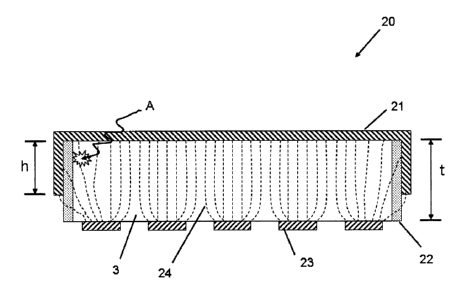
The basic example version of a pixilated radiation detector 20 is illustrated
in Fig.3 in cross-section. A single crystal tile 3 of CdZnTe is provided as a
rectangular
slab with major opposing surfaces as is common in the industry, and having
thickness t.
Typically the tile is substantially rectangular in shape. It may be square
with equal rows
and columns of pixels, but may also be any geometric shape required by the
imaging
application. An encapsulant or insulator 22 is applied on sides of the tile 3.
In the
preferred case the insulator is applied on the entire side for ease of
processing. An
anode pixilated array 23 is formed on the major surface positioned to be
opposite the
incident radiation, for the purpose of collecting generated charge and forming
a 2D
image from pixel responses. Pixels are defined as equivalent to anode segments
having
any geometric shape and, in the preferred case, pixels may be substantially
square. For
illustrative purposes, the side-shielding cathode electrode 21 is shown as a
continuous
single conductor. In fabrication as will be described later, this may in
effect be applied in
two portions, the first directly on the tile surface opposing the pixilated
anode array 23,
and the second side portion extending over the tile sides and partially
covering the
insulator 22. Preferably the insulator encapsulates the full surface of the
sides without
contamination. However, in alternate embodiments it may also be separated in
two
CA 02541256 2006-02-22
insulating portions. The side portion of the side-shielding cathode 21 extends
a height h
as shown from the cathode plane (major surface) of the tile towards the anode
plane of
the tile. The height can be maximized to provide shielding and field shaping
but is
preferably adequately limited to reduce shorting between anode and cathode
when a
5 bias voltage is applied between them. For the case of Cadmium Zinc Telluride
semiconductor and gold conductor, the preferred height is within the range of
approximately 40-60% of tile thickness. It was observed that at a height at
70% of
thickness the surface leakage current significantly increased. The effect of
side
electrode height is shown in Table 1. In the case of a typical 5mm thick
detector, the
10 preferred side shield portion extends - 2.5-3mm.
Electric field lines are shown as dashed lines, and were derived using
standard techniques similar to the prior art illustrations in the background.
The field lines
demonstrate improved field confinement over unshielded, guard ring and third
electrode
15 designs. During operation as a radiation detector, generated charge near
the edges of
the tile from an incident radiation wave is partially collected at the closest
anode with
higher efficiency than alternative detector corrective designs. In the
preferred example
for CZT semiconductor, the electrodes are gold and the insulator is polymer
encapsulant such as Humiseal. Alternatively, the insulator may be an oxide or
similar,
formed by physical deposition. The gold electrodes may be formed by an
electroless
process additionally.
The side-shielding cathode design ensures the resulting device leakage
current, and the surface leakage current in particular, does not increase to
an excessive
level as often observed with multi-electrode designs. The fabrication method
of the
invention does increase leakage current but at a much reduced rate relative to
known
fabrication methods if surface stoichiometry is maintained. This minimizes
electronic
noise and gives good detector energy resolution, especially from the edge
pixels. More
importantly, the low surface leakage current characteristic implies low
surface
CA 02541256 2006-02-22
16
conductivity which in turn means reduced electric field line bending in the
side shielded
cathode detector. The field is therefore more confined within the bulk
semiconductor.
Additionally, the extended shielding design of the cathode further ensures the
field lines
around the edge of the detector are well focused into the edge pixels,
resulting in a
significant reduction of charge loss and subsequently improved charge
collection
efficiency of the edge pixels.
Fig.4 illustrates a perspective cutaway of a monolithic detector 35 of an
embodiment of the invention. Pixilated anode array 36 covers the upper major
surface
and the side portion 21 of side-shielding cathode is shown. Insulator 22 not
covered by
the side portion protects the side surface and isolates an electrical path
from anode
pixels to side cathode. In an alternate embodiment, the anode pixels extend
right to the
edge of the anode surface of detector 35. The dimensions of the imaging array
are
determined by application requirements. In general, the pixel array may be m
by n
pixels. Common array dimensions for Gamma and X-ray detectors are 8 x 8, 11 x
11
and 16 x 16. Typical tile sizes for CZT detectors are 20 x 20 mm or 40 x 40mm.
The
side-shielding cathode can be implemented in any tile size or array
dimensions. With
common configurations, the percentage of edge and adjacent-to-edge pixels is
substantial, and edge performance improvement results in a dramatic overall
imaging
performance by the detector.
The performance of the side-shielded cathode detector varies with the
height of the side portion of the cathode as described earlier. For the
preferred case of a
CZT semiconductor tile and gold electrodes, the side cathode depth was varied
to
determine the optimum range, with a summary of results indicated in Table 1
below.
The tile example has an anode array of eight by eight pixels for a total of
sixty four.
Typical performance metrics include energy resolution and total surface
leakage as
commonly measured by standard techniques in the radiation detection industry.
As
expected, the surface leakage current increases with the area of the cathode
conductor,
CA 02541256 2006-02-22
17
and a tradeoff is sought between an acceptably small increase in surface
leakage
current for relatively large improvement in the number of pixels with energy
resolution
less than 6% FWHM. The ER parameters reached an optimum at 3mm side cathode
depth with a high yield of 63 out of 64 pixels demonstrating FWHM < 6%. At the
optimum depth, bias voltage was successfully increased to 2000V without
tunneling or
shorting of the electrodes. At increased depth, the surface leakage current
increased
dramatically to unusable levels. For the preferred height of 3 mm, the surface
leakage
current per pixel is low, approximately 210/64 = 3.3nA/pixel.
Table 1 ER and SLC as a function of side cathode depth
Cathode Side Shield on 5mm # of pixels with ER Total Surface Leakage
thick CZT tile FWHM < 6% Current (64 pixels)
@ 1500V bias
Side shield depth (mm) (nA)
0 (none) 0 27 80
1.5 8 34 150
2 22 57 165
2.5 27 61 180
3 28 63 210
3.5 26 61 900
Much higher charge collection at the edge pixels occurs in the side-
shielding cathode design, and the corner regions near the cathode side are
fully active
(in terms of charge collected from events near the corner regions). Note,
there are no
additional electrodes required beside the cathode and anode, as the cathode is
configured in a novel manner. However, due to the insulating layer on the side
surfaces
of the detector underneath the side shielding portion of the cathode, new
fabrication
CA 02541256 2006-02-22
18
techniques were required. Reliable and economical methods of fabricating the
device
and insulating layer are provided (for example in Fig.13).
Preferably the cathode side portion is continuous, encircling all sides of
the tile. However, for esoteric detector configurations the side portion may
be
discontinuous for portions where the pixels are spaced inwards or there are no
pixels
proximal to the tile edge, for example in a non-rectangularly-shaped tile. For
all
embodiments, the side portion of the cathode is insulated from the
semiconductor.
It is illustrative to show the effect of the side-shielding cathode on leakage
current as conventional understanding would expect a significant increase in
leakage
current as the total area of the cathode is increased by a substantial amount.
The
leakage current is a broad measure of the electrode performance, and
demonstrated in
the detector I-V plot of Fig.5 under bias potential for both a shielded and a
conventional
cathode design. The side-shielding cathode current is slightly higher than for
the
unshielded but the increase is minimal and acceptable because of the greatly
improved
charge collection efficiency.
Specific improvements of the electrode design performance are
demonstrated on a pixel by pixel response basis under gamma radiation testing
to
compare the side-shielded embodiment to a conventional detector. In Fig. 6,
gamma
radiation response is shown for each pixel in an unshielded detector similar
to the
embodiment in Fig.1 b(no side shielding). The radiation source was Co-57;
(Main
measured photopeak at 122 keV), bias voltage 500V. The irradiation is nearly
uniform
across the whole cathode surface of the pixilated detector. The test samples
were
configured as 8x8 pixels on a 20x20x5mm detector. Radiation performance data
is
shown for each pixel as measured by energy resolution (ER) and peak count
(PC), as
commonly defined in the radiation industry. The graphs show sharp and high
energy
peaks in the center pixels, but reduced peak count and increased peak width in
the
CA 02541256 2006-02-22
19
edge and adjacent-to-edge pixels. The most dramatic performance degradation is
evident in the corner pixels as expected due to the field line bending and
reduced
charge collection efficiency.
For this conventional design baseline example, as shown at pixel B, the
corner pixel (worst case) is measured to have;
ER = 11.7%
PC = 150
For comparison, as shown at pixel C, an inner corner pixel is measured to
have performance better than the corner pixel but still degraded relative to
the inner
central pixel performance;
ER=7.6%
PC = 310
Exemplary Embodiment Performance:
The previous unshielded results are compared to a radiation detector with
the modification of side-shielded cathode embodiment of Fig. 9, with test
results as
shown in Fig. 7. The CZT detector configuration corresponded to the
conventional
baseline example for array and tile dimensions. Tile thickness was 5 mm, the
anode
array was 8 x 8 pixels, and the electrodes were gold, the side insulator was
Humiseal
polymer and the side portion extends 2.5-3mm. The radiation source was Co-57;
radiation energy 122 keV and bias voltage 500V. In general, a dramatic
improvement in
the FWHM energy spike on the outer pixels is demonstrated, and improved peak
counts. Both of these measures improve signal-to-noise and the quality of the
derived
signal. Improvements in charge collection efficiency result in improvements in
both
CA 02541256 2006-02-22
energy resolution and peak counting efficiency, as shown. The side-shielding
cathode
detector improves both outer corner pixels (typically affected the most by
shielding) and
also adjacent-to-outer row pixels. Correcting the total surface leakage
current for pixel
dimensions, the detector leakage current density was typically less than 6
nA/mm2, as
5 measured at a bias potential of 1400V.
For example as shown at pixel D, the improvement in the corner pixel is
measured as;
ER = 5.2%
10 PC = 308
For example, as shown at pixel E, the improvement in the inner corner
pixel is measured as;
15 ER=6.5%
PC = 354
Therefore the side-shielding cathode detector is demonstrated to
significantly improve the metrics of energy resolution and peak count.
Specifically, the
20 energy resolution is reduced by a factor 2 for the example corner pixel,
showing
increased charge collection efficiency for improved correlation to ionizing
radiation
energy. The corner pixel peak count is also approximately doubled, improving
signal-to-
noise and enabling lower thresholds of ionizing radiation energy to be
detected. As the
corner pixel is expected to gain the most, it is instructive to compare an
inner corner
pixel E. The inner corner pixel shows a reduced impact of about 20%
improvement but
demonstrates the improvement extends to the next row of pixels. Non-corner
edge
pixels additionally are improved as shown. The improvements are typical of
relative
enhancements observed in repeated experiments using CZT semiconductor of
various
grades.
CA 02541256 2006-02-22
21
The improved performance is consistently observed across multiple
samples and edge pixels, for the preferred CZT detector design. The
repeatability and
reliability of performance was tested over 10 typical samples, with and
without the side-
shielding cathode and the test data is shown in Fig. 14, for peak count and
energy
resolution. There was variability sample to sample depending on bulk CZT
selected,
and fabrication process, however in the majority of samples the relative
enhancement
was dramatic, particularly for the outer pixel performance. A good energy
resolution is
less than 6% for the energy peak tested, and the average improvement in the
number of
pixels reaching that target was over 400% for the outside pixels. In terms of
overall
pixels, still a dramatic 200% improvement was recorded. Segmented detectors
with the
side-shielding cathode therefore can produce energy resolution (full-width-at-
half-
maximum) for more than 90% of the pixels under 6%, in response to gamma
radiation.
Average peak count improvement of the edge pixels was about 20%. This enhanced
detector response results in significant yield improvement of commercially
usable
devices.
In the preferred embodiment, the side insulating layer is a polymer
encapsulant such as Humiseal. However in an alternate embodiment an oxide may
be
used which can withstand higher temperatures. This may be advantageous when
energetic deposition methods are used for all or portions of the cathode
electrode, such
as sputtering. Radiation detector 40 is illustrated in Fig. 8 with an oxide
insulator. Single
crystal CdZnTe 3 is coated with the oxide layer 41 on the sides, which may be
physically deposited by e-beam or thermal evaporation, then a mask is applied
and the
oxide layer 41 covered partially by side-shielding cathode layer 21. The
effect is not
very sensitive to the thickness of the insulating layer, however it must have
a minimum
thickness to be properly insulating as is well known in the semiconductor art.
This
embodiment permits the side-shielding cathode to be fabricated as one integral
continuous layer.
CA 02541256 2006-02-22
22
Fabrication of CZT detectors with high performance is complex as is
evident by the large body of research published. Surface effects resulting
from
fabrication and materials selection have been shown to have a critical impact
on device
performance. The challenges of fabricating the side-shielding electrode in CZT
with gold
electrodes have been solved by novel fabrication methods and using multiple
depositions to form a unitary cathode with side portions, suitable for high
performance.
Figures 9-12 show various embodiments for the side-shielding CZT detector,
which can
also be applied or extended to other radiation semiconductor materials.
In an alternate embodiment the side-shielding cathode can be formed as
two conductor layers, as detector 50 shown in cross-section in Fig. 9. Single
crystal tile
3 has pixilated anodes 23 formed on one major surface. Insulator 22 is formed
on the
tile sides. First conductor layer 51 covers the major surface opposing the
anode pixels.
A second conductor layer 52 coats the first conductor layer and extends over
the tile
sides as shown. This design is advantageous when the optimum process for
surface
coupling of conductor 51 to the semiconductor surface is deficient in terms of
providing
an adherent uniform layer on the side surface. For example, providing an
adherent gold
layer by electroless process on Humiseal insulator coating is challenging due
to the
acidic properties of the process solutions. Hence two different deposition
processes
may be used for each cathode portion, as will be discussed in the method
description.
Preferably the two cathode conductor layers are identical i.e. both gold, but
may
alternatively be different conductors reasonably matched for similar
electrical properties.
Fig. 10 shows an alternate embodiment of the side-shielding cathode
formed from two conductor segments, for detector 60 shown in cross-section.
First
cathode conductor layer 61 covers all of the major tile surface. A second
conductor
layer 62 is formed to butt against layer 61 for excellent conduction, and to
extend over
the peripheral surface around the central portion, as well as over the tile
sides and
CA 02541256 2006-02-22
23
insulator 22. For example, the first conductor layer 61 could be fabricated by
electroless
gold deposition and the second conductor layer 62 could be deposited by
sputtering
gold, with appropriate masking of tile portions.
A further embodiment of the two portion side-shielding cathode detector is
shown in Fig. 11. A cross-section of a monolithic radiation detector 70 has an
overhanging cathode formed of conductor layers butted together to form a
single side-
shielding cathode. First cathode conductor layer 71 covers a central portion
of the tile
surface. A second conductor layer 72 is formed to butt against layer 71 with a
low
resistance interface, and to extend over the peripheral surface around the
central
portion, as well as over the tile sides and insulator 22. For example, the
first conductor
layer 71 could be fabricated by electroless gold deposition and the second
conductor
layer 72 could be deposited by sputtering gold, with appropriate masking of
portions of
the semiconductor tile.
For use in a radiation detector subassembly, the radiation detector must
be electrically connected to signal processing circuit boards, without
modifying the
electrode properties substantially. An intermediary conductor layer(s) may be
formed on
the anode pixels to reduce deleterious electrical contact effects and thermal
damage to
the anode pixel. As is illustrated in Fig. 12, a radiation detector 80 with
side shielding
cathode 21 is shown with a tri-layer contact on top of the anode pixels, for
suitable
contacting detector boards to detector pixels by thermal contacting.
Preferably the
contact layer is smaller than the anode area. The trilayer contact is expanded
in view
G, showing a platinum layer 81, a nickel layer 82 and a sputtered gold layer
83.
Alternatively titanium or other conductors may be used, or fewer or more than
three
layers.
Fabrication Processes
CA 02541256 2006-02-22
24
There are several acceptable processes for fabricating a CZT radiation
detector with side-shielding cathode, with varying process complexity and
device
reliability. These are described for the preferred materials demonstrated in
the
experimental results, but can be extended substituting known processes for
substitute
materials. It was found that contamination of the encapsulant/insulator
applied to the
semiconductor tile sides, was critical to control for reduced surface leakage
and
preferred I-V characteristics of the detector under bias voltage. A sub-method
is
provided that controls contamination in the side insulators, partly enabling
the excellent
low surface leakage current reported. In general, a polymer encapsulant is
preferred
due to ease of processing, but requires adjustment of the other steps of the
fabrication
process.
Method I is used to fabricate a cathode in one primary cathode deposition
step. The steps in method I are i) preparing a tile with anode pixels on one
major
surface and polymer encapsulant on all sides, ii) applying a mask shielding at
least 30%
of the Humiseal on the sides extending from the anode surface, iii) depositing
a unitary
gold layer over the opposing major surface and unmasked Humiseal to form an
integral
cathode with side-shielding portion. This method requires overcoming the
challenge of
optimizing the gold deposition process to have suitable cathode adhesion to
both the
CZT and the polymer encapsulant, and not melting the Humiseal. An alternate
version
of this method has step i) modified to physically deposit a high temperature
oxide on the
tile sides as the encapsulant, then in step iii) the deposition process can be
electroless
gold. Yet another embodiment can use a high temperature polymer encapsulant
(not
Humiseal) that will provide suitable gold adhesion following the electroless
gold
deposition process.
Method II applies an electroless gold process to deposit a first thick
cathode layer on the tile major surface and then energetic deposition of a
second thin
side cathode layer on at least the side portions, the two layers coupled to
form the side-
CA 02541256 2006-02-22
shielding cathode. The steps of Method II are shown in Fig 13. As a starting
condition a
bulk semiconductor tile (for example CZT) is cut and polished on all sides. In
step 100,
thick electrodes are deposited on at least the front and back of the
semiconductor
crystal tile. This may be done by physical deposition or electroless
deposition provided
5 suitable adhesion to the device surface is achieved. A process for
electroless deposition
of gold onto CZT with excellent adhesion is described in co-pending patent
application
"Radiation detector device with high performance and high interpixel
resistance
fabricated using electroless gold deposition", incorporated herein by
reference. Then in
step 110, masking and etching a pixel array on one electrode surface forms an
anode
10 array. Again, with reference to the co-pending application, a bromine
solution etching
method with low interpixel resistance is preferred, although alternate known
etching
processes may be substituted. In step 120, a dielectric encapsulant is applied
to at
least the sides of the tile. The preferred insulator is the encapsulant
Humiseal, well used
within the industry. This polymer-based solution is applied by either dipping
(preferred)
15 or brushing/coating the solution to cover the sides of the tile. The coated
tile dries for
several hours in a clean environment to maintain low contamination levels. In
step 130,
a portion of the sides of the tile is masked, the mask extending from the
anode plane
out a fraction of the tile thickness. For the example of a 5mm thick CZT tile,
2.5 mm
copper tape with adhesive can be uniformly wrapped from the beginning of the
anode
20 plane to approximately midway up the tile sides. Then in step 140, a second
conductor
layer is deposited onto the unmasked side portions and on at least a portion
of the
cathode to form a side-shielding cathode (as configured in one of the
embodiments
shown in Fig 9,10 & 11). The preferred second deposition process is sputtering
a gold
layer, as the electroless gold solution of the co-pending application will
dissolve the
25 Humiseal polymer encapsulant , and thermal evaporation of gold has poor
adhesion to
the polymer encapsulant. The sputtered gold layer may be on the order of 50-
100nm or
thicker, and may cover parts or the entire major cathode layer from step 100
(per
configurations in Figs 9-11). Optionally, prior to step 140, the surface
leakage current of
the device can be tested and if not adequate due to surface effects or
fabrication
CA 02541256 2006-02-22
26
variation, additional side polishing of the tile and repeating of earlier
steps may be
carried out to ensure a low intrinsic surface leakage current before the final
coating
step.
Alternatively, the insulator in Method II may be a high temperature oxide
deposited by conventional physical deposition. In this embodiment, the
deposition
process in step 140 allows physical deposition methods to replace the
sputtering
process, if desired. For example, an oxide layer of about 100nm is suitable.
Similarly,
the second conductor layer may not be matched to the primary cathode
conductor, but
be suitably matched in conductivity, thermal expansion etc.
Method III proceeds through steps 100-130 of Method II, and then
substitutes a physically-secured conductor tape which is electrically soldered
to the
primary cathode layer of step 100. In this method step 130 is replaced by
taping an
adhesive conductive tape (copper preferred) in the prescribed desired location
of the
side cathode shield extending from the cathode major surface plane down
approximately halfway in the tile thickness. The adhesive layer can be used as
a
suitable insulator. Step 140 is replaced by soldering the copper tape to the
thick primary
cathode layer to form an electrically common side-shielding cathode. This
process is
convenient but challenged by the conductor mismatch, micro-variation in tape
contact
and maintaining insulator adhesive thickness near the solder connection at the
edge of
the tile.
The detector tile arrays described herein may further be assembled side-
by-side in a close-packing arrangement as the cathodes of all the tiles in a
large
assembly of arrays of pixels are all at the same bias potential.
CA 02541256 2006-02-22
27
The reader will appreciate that the foregoing description is only intended
to be illustrative of the present invention and is, therefore, not to be
construed as a
limitation or restriction thereon, the invention being delineated in the
following claims.