Note: Descriptions are shown in the official language in which they were submitted.
CA 02542093 2006-04-06
OPTICAL MICRORESONATOR COUPLING SYSTEM AND ASSOCIATED METHOD
Field of the Invention
The present invention relates to the field of
optical resonators, and more particularly, to optical
microresonators that exhibit whispering gallery modes.
Background of the Invention
Telecommunications systems incorporate extensive
optical fiber networks using frequency
multiplexing/demultiplexing techniques for optical
communications signals. These types of optical communications
systems require add/drop filters for selecting a single
wavelength from complex optical signals that are typically
frequency multiplexed together. Also, optical sensors are
used at narrow band frequencies and wavelengths and may
require add/drop or other functionality. These sensors are
required for accelerometers, chemical and biological sensors,
and similar applications.
Prior art devices for these add/drop filters and
optical sensors include Fabry-Perot structures, waveguide ring
resonators, and spherical resonators. Fabry-Perot structures
have been widely used for many applications, but have
difficult extensions to the multipole. Waveguide ring
resonators are planar structures that can be fabricated with
little complexity and incorporate a simple extension to the
multipole. One drawback is their high losses. Spherical
resonators are small in size and have low loss, making them
efficient for limited applications. They are not efficient,
however, for some applications requiring an extension to
multipole filters. Other microcavity geometries incorporate
whispering gallery modes and photonic crystals.
FIG. 1 shows a prior art microsphere 20 positioned
adjacent an optical fiber 22. A 980 nm SMF and 980 nm optical
-1-
CA 02542093 2006-04-06
pump are used as an input and the output is a 1550 nm SMF and
1550 nm laser. The optical fiber 22 is tapered and can be
brought in contact with the microsphere 20 and the evanescence
light from the optical fiber 22 enters the microsphere 20.
Air guided region 24 and vestigial cores 26 are shown. The
TEill mode of propagation occurs along the "equator" or center
portion of the microsphere. This is a well known practice
operative in a whispering gallery mode.
Other examples of prior art microspheres operative
in a whispering gallery modes have been designed. For example,
U.S. Patent Nos. 6,389,197; 6,487,233; and 6,490,039 assigned
to California Institute of Technology, disclose the use of
microspheres based on whispering gallery mode microresonators
or cavities. An optical probe can be evanescently coupled
into at least one whispering gallery mode of the resonator.
Optical energy can also be coupled in a waveguide mode, into
the resonator that operates in the whispering gallery mode.
For example, a fiber in its waveguide mode would couple
information to the resonator, e.g., the microsphere. The
fiber can be cleaved at an angle to cause total internal
reflection within the fiber. The energy in the fiber forms an
evanescent field and the microsphere is placed in the area of
the evanescent field. If the microsphere resonance is
resonant with energy in the fiber, information in the fiber is
effectively transferred to the microsphere. Surface gratings
can also be placed on the microsphere. This is advantageous
because microsphere resonators can have high quality ("Q")
factors and small dimensions. They can be a building block
for larger fiber optic systems. It is also possible to have a
fiber-coupled laser based on a whispering gallery mode
resonator formed of a laser gain medium and an angle-polished
fiber coupler as disclosed in the '233 patent. The optical
fiber can be configured to guide light at both the pump
wavelength and a laser wavelength,, including an angle-polished
-2-
CA 02542093 2006-04-06
facet that forms an angle with respect to the fiber such that
the angle-polished facet is positioned with respect to the
other resonator to couple evanescently pump light at the pump
wavelength in the optical fiber into a whispering gallery mode
at the pump wavelength, and also evanescently couple light in
a whispering gallery mode at the laser wavelength into the
optical fiber.
One prior art improvement over the use of
microspheres are toroid microcavities. These microcavities
can have ultra-high "Q" factors of about 100 million and a
surface-tension induced microscale cavity. Examples include
droplets, silica microspheres, and microtoroids.
Toroid microcavities have been formed by
photolithography and etching techniques on an oxidized silicon
wafer to create silica disks. A gas XeF2 etch undercuts the
silica disks with an induced reflow of the silica using COz to
cause a smooth toroidal periphery. Toroid microcavities
support whispering gallery type modes on a silicon platform
and can reduce the mode spectrum compared to spherical
microcavities. Microtoroids can also exhibit reduced mode
volume compared to microspheres. Two mode-volume compression
regimes can include slow compression and fast modal
compression.
In a tapered fiber coupling, the fiber tapers in a
transition from conventional core guiding regions to air-
guiding regions with a vestigial core on either end as shown
in FIG. 1. It can include coupling both to-and-from a
microtoroid on a chip.
These ultra-high "Q" factor and small mode volume
results in high circulating intensities because of the cavity
build-up factor. Optical fibers that are tapered result in an
ultra-low loss and optimum coupling of the microcavities. The
cavity build-up factor and non-linear threshold level can be
exceeded as indicated from the equation below:
-3-
CA 02542093 2006-04-06
Qex
P,.n = ~c2nR . Q 2
1 + Qo
Pin = 1 mW Pcirc ~ 110 W
V~, '650 /1m3 Icirc "'2.5 GW~Cmz
There have also been some experiments on stimulated
Raman scattering in microspheres. The stimulated Raman
scattering causes red shift of a pump (100 nm shift in a
telecommunications band). Threshold levels can be typically
100 microwatts for UHQ microtoroids and high quantum
efficiencies result because of an ideal coupling junction.
Similar results can occur with toroid microcavities. The
stimulated Raman scattering for toroid emission is typically
single mode.
A prediction of threshold using bulk Raman gain
constant (doubly resonant process) can be:
_ ~ZnZ~ell P
thresh ~,P~Rfg~~r ~ ~ ~ex t a 2
A minimum threshold undercoupled could be:
~~in = 2Q0~~ T~ ll%~
The Raman threshold can also affect the mode volume
as follows:
Veff - thresh ~ ~o ~P~R~gyr ~ 4
~ n 27
-4-
CA 02542093 2006-04-06
P: Raman threshold
pump and Raman emission wavelength
g: Raman gain coefficient
C(r ): intermode coupling parameter
Q: Quality factor of pump and Raman mode
Stimulated Raman threshold can be used to infer the
mode volume Veff .
- pmin ~ 2 ~P~Rfg~(r )
efj thresh ~o ~2 n 2
Although spherical resonators, waveguide ring
resonators, Fabry-Perot structures and toroid microcavities
have been advantageously used as indicated above, these
devices still have limitations when optical fibers are
coupled, even though these devices often are easily
fabricated.
Published patent application no. US 2002/0041730,
published April 11, 2002, discloses a method for fabricating
an optical resonator on an optical fiber by generating a
differential of a physical property, for example, the
diameter, density, refractive index, or chemical composition
of a transverse segment of the resonator fiber. This could
include some type of grooves forming the resonators. The
resonator fiber segment can substantially confine a
circumferential optical mode propagating around the resonator
fiber segment circumference at least partially within the
resonator fiber segment. This enables substantial confinement
of a substantially resonant circumferential optical mode near
a surface of the fiber. As a result, evanescent optical
-5-
CA 02542093 2006-04-06
coupling can occur between circumferential optical modes and
an optical mode supported by the second optical element.
Different techniques for spatially, selectively generating the
differential could include masking/etching,
masking/deposition, laser machining, laser patterning and
combinations of the different processes. It is also possible
to include a plurality of resonators in the same fiber
sufficiently close together to enable optical coupling between
them to provide a frequency filter function for optically
coupling multiple optical elements, including optical fibers.
Although the optical resonator can provide some coupling, it
is limited in its use and may not provide adequate coupling
for input/output functions. Its manufacturing requires non-
rotating upper and lower capillary tubes to hold a spinning
optical fiber, which may not ensure accuracy and have excess
tolerance. Some limited teaching for using a single, tapered
optical fiber near the microcylinder is also proposed. It
also does not address polarization issues, slower waveguide
structures, multiple node contacts, and the use of coatings
for imparting waveguide resonance or similar issues.
Summary of the Invention
In view of the foregoing background, it is therefore
an object of the present invention to provide an optical
microresonator coupling system that can be operative with
optical source waveguides and optical exit waveguides and form
an input/output device such as a filter.
This and other objects, features, and advantages in
accordance with the present invention are provided by an
optical microresonator coupling system that includes an
optical source waveguide through which light travels. A
microcylinder is positioned adjacent the optical source guide
and has a resonant waveguide formed from spaced resonant
elements, such as circumferential ridges, and a diffractive
-6-
CA 02542093 2006-04-06
coating thereon, which optically couples light from the
optical source guide onto the microcylinder. An optical exit
waveguide is positioned adjacent to the microcylinder and
spaced from the optical source waveguide and couples light
from the microcylinder into the optical exit waveguide.
In one aspect of the invention, the microcylinder is
tapered along the resonant waveguide such that the
microcylinder can be moved axially relative to the optical
source and exit waveguides for tuning at a selected frequency.
The optical exit waveguide can also be positioned adjacent the
microcylinder opposite the optical source waveguide. Both the
optical source and exit waveguides can be formed as optical
fibers that could be aligned axially or substantially
transverse to the microcylinder. The optical fibers are
preferably single-mode optical fibers.
In another aspect of the invention, the resonant
waveguide can be formed as a plurality of spaced ridges that
are formed parallel or in a spiral. The microcylinder can be
tapered such that the ridges provide tuning.
In another aspect of the invention, the optical
source waveguide and the optical exit waveguide can be
operative as a four-port optical microresonator coupling
system. Coupling elements can be formed on the resonant
waveguide and operative therewith for optically coupling light
from the optical source waveguide and changing light direction
on the microcylinder. These coupling elements can be angled
for changing light direction a predetermined amount. The
optical source waveguide and optical exit waveguide can both
be transitioned to a core.
Brief Description of the Drawings
Other objects, features and advantages of the
present invention will become apparent from the detailed
CA 02542093 2006-04-06
description of the invention which follows, when considered in
light of the accompanying drawings in which:
FIG. 1 is a fragmentary drawing of a prior art
microsphere positioned adjacent an optical fiber to provide
coupling between the optical fiber and microsphere.
FIG. 2 is a graph showing a tap field strength
weight distribution with delay of an impulse response for a
Gaussian filter and showing the filter response relative to
the frequency offset.
FIG. 3 is a graph showing the impulse response of a
10 GHz bandpass Gaussian filter and showing the field coupling
weight relative to the delay in millimeters of glass.
FIG. 4 is a graph showing the band shape for
Gaussian and Butterworth filters.
FIG. 5 is a fragmentary elevation view of a single
mode, four-port optical microresonator coupling system in
accordance with one example of the present invention.
FIG. 6 is a fragmentary side elevation view showing
an optical microresonator having a resonant waveguide formed
on a microcylinder, and formed from coupled resonators as
circumferential ridges in accordance with one non-limiting
example of the present invention.
FIG. 7 is a high level flowchart illustrating a
method of forming the resonant waveguide as coupled resonators
on the microcylinder, for example, as shown in FIG. 6, in
accordance with one example of the present invention.
FIG. 8 is a fragmentary, partial isometric view of
an apparatus used for forming the resonant waveguide on a
microcylinder, in accordance with one example of the present
invention.
FIG. 9 is a graph showing a modeled whispering
gallery mode on a microcylinder and showing the field strength
relative to the distance from the surface in microns in
accordance with one example of the present invention.
_g_
CA 02542093 2006-04-06
FIG. 10 is a graph showing a modeled ridge-guided
wave on a microcylinder of the present invention and showing
an axial distance in microns relative to a radial distance in
microns.
FIG. 11 is a fragmentary side elevation view of a an
optical microresonator coupling system used as a filter and
showing a microcylinder having a resonant waveguide formed on
a microcylinder in accordance with one example of the present
invention.
FIG. 12 is a graph showing steady state field
patterns in accordance with one example of the present
invention and showing the field strength relative to the
distance from the waveguide axis in microns.
FIG. 13 is a graph showing transient field patterns
in a source waveguide and the distance from the waveguide axis
and time in picoseconds in accordance with one example of the
optical microresonator of the present invention.
FIG. 14 is a graph showing transient field patterns
in an optical microresonator have a resonator waveguide in
accordance with one example of the present invention and
showing distance from the waveguide axis in microns relative
to the time in picoseconds.
FIG. 15 is a fragmentary side elevation view of an
optical microresonator coupling system and showing optical
source and exit waveguides located close to the optical
microresonator.
FIG. 16 is a fragmentary side elevation view of a
plurality of optical microresonators coupled together and
forming a coupled waveguide, microresonator structure in
accordance with one example the present invention.
FIG. 17 is a fragmentary isometric view showing an
optical microresonator that includes a resonant waveguide and
coupling element of the present invention.
-9-
CA 02542093 2006-04-06
FIG. 18 is another fragmentary, isometric view
showing an optical microresonator that has a wide contact,
unguided resonator waveguide and coupling element of the
present invention.
FIG. 19 is a fragmentary side elevation view of two
microcylinders each having a spiral resonant waveguide and
forming a slow-wave optical microresonator of the present
invention.
FIG. 20 is a graph showing an EMP model frequency
response for a 10 micron silica microcylinder showing the
resonant waveguide transfer function on the vertical axis and
the wavelength in nanometers on the horizontal axis in
accordance with one example of the present invention.
FIG. 21 is a graph similar to FIG. 20, but showing
an EMP model frequency response of a 30 micron silica
microcylinder and showing in greater detail the axial and
radial pole modes remaining separated for all diameters in
accordance with the present invention.
FIG. 22 is a fragmentary elevation view of a coated
microcylinder of about 9.5 micron with a 0.4 micron polymer
coating to form an optical microresonator in accordance with
one example of the present invention.
FIG. 23 is a graph showing an EMP model frequency
response for a 9.5 micron silica microcylinder coated with a
0.4 micron polymer having a 1.55 index to form an optical
microresonator in accordance with one example the present
invention.
FIG. 24 is a graph showing a Finite Difference Time
Domain (FDTD) model and showing the insertion loss of an
optical microresonator similar to that shown in FIG. 22 and
used as a drop filter in accordance with one example of the
present invention.
-10-
CA 02542093 2006-04-06
FIG. 25A is a diagram showing two coated, uncoupled
optical microresonators used as a drop filter in accordance
with one example of the present invention.
FIG. 25B is a graph showing a finite difference time
domain model with the insertion loss for the two uncoupled
optical microresonators used as a drop filter in accordance
with one example of the present invention.
FIG. 26 is a graph showing the response of an
optical microresonator formed from a microcylinder having a
300 nanometer thickness film with an index of 1.55 and showing
the optical source waveguide throughput and optical exit
waveguide output, and a filter transfer function (FTF) in
decibels as a function of wavelength in nanometers.
FIG. 27 is a graph similar to the graph of FIG. 26,
but showing the optical source waveguide throughput and
optical exit waveguide output for the 400 nanometer thickness
sample.
FIG. 28 is a graph similar to FIGS. 26 and 27 for
optical source and exit waveguides, but showing a 500
nanometer thickness.
FIGS. 29-31 are graphs similar to FIGS. 26-28, but
with microcylinders having with a film index of 1.50 instead
of the film index of 1.55, as in graphs shown in FIGS. 26-28.
Detailed Description of the Preferred Embodiments
The present invention will now be described more
fully hereinafter with reference to the accompanying drawings,
in which preferred embodiments of the invention are shown.
This invention may, however, be embodied in many different
forms and should not be construed as limited to the
embodiments set forth herein. Rather, these embodiments are
provided so that this disclosure will be thorough and
complete, and will fully convey the scope of the invention to
those skilled in the art. Like numbers refer to like elements
-11-
CA 02542093 2006-04-06
throughout, and prime notation is used to indicate similar
elements in alternative embodiments.
The present invention is advantageous over prior art
spherical resonators, waveguide ring resonators and Fabry-
Perot structures, including toroid microcavities, and simple
cylindrical resonators as described in the incorporated by
reference '730 published patent application. The present
invention is directed to an optical microresonator that
includes a resonant waveguide formed on a microcylinder, for
example, spaced resonant elements, such as circumferential
ridges, forming a resonant waveguide on the microcylinder for
coupling to and from optical input and exit waveguides. These
resonant elements could include ridges, some types of grooves,
etched surface configurations, dielectric lines or other
dielectric placements, or coatings. Whispering gallery modes
on a microcylinder can use a one-dimensional beam propagation
coating and an effective index profile to account for a
cylindrical geometry, for example, with a 120 micron
microcylinder, n=1.498, Gaussian mode with 8.3 micron mode
field diameter, on right microcylinder and immersed in water,
n=1.33. For purposes of explanation, basic functions of a
resonant waveguide on a microcylinder in accordance with one
non-limiting example of the present invention are explained.
A waveguide on a microcylinder can form a homogenous
waveguide structure and can be extended to complex, coupled
structures. Although prior art microsphere technology is a
simple, natural geometry and readily available because of its
wide application in biochemistry and as a filler with
concomitant ease of fabrication, microspheres are difficult
structures for use in compound/multipole structures.
Microcylinder resonant waveguides of the invention can be
formed by ultraviolet laser writing on a rotating
microcylinder, for example, by cutting ridges or exposing to
-12-
CA 02542093 2006-04-06
light a photoresist-coated microcylinder, as will be explained
in greater detail below.
In the present invention, light impinges on the
microcylinder having the resonant waveguide and can be
considered to be guided around the curved surface forming the
microcylinder without lateral guidance. In one example of the
present invention, however, lateral spreading is prevented by
using the resonant waveguide on the microcylinder and
confining the energy and preventing the energy from moving
axially down the microcylinder and then spreading. In some
aspects of the present invention, depending on the
configuration, it is possible to place spaced, circumferential
ridges on the microcylinder, forming resonant elements, e.g.,
resonators, and thus forming a resonant waveguide. It is also
possible to place a layer of glass on top of the microcylinder
to form a resonant waveguide. Circumferential spaced ridges
as resonators can also be placed on the glass. In other
aspects of the present invention, it is possible that light
can move around the microcylinder against its surface and
ridges or an extra layer is not required.
In some cases, it is desirable to etch the
circumferential ridge for the resonant waveguide around the
microcylinder. In one non-limiting example, a collar of
photoresist could be placed on the fiber, which is chemically
etched at a fraction of a micron, enough to form a resonant
waveguide. The photoresist could be exposed to light from a
laser, for example. When the photoresist is stripped off,
that fiber area that has not been etched is untouched glass
and forms a resonant waveguide. It is also possible to couple
two microcylinders together using precise lithographic
techniques. It is also possible to control the height of any
ridges and control the coupling between resonators forming the
resonant waveguide of the optical microresonator. Two coupled
resonators or ridges could be formed on the same
-13-
CA 02542093 2006-04-06
a
microcylinder, for example, an optical fiber, by writing two
lines or ridges and etching the devices, as compared to
difficulties in the prior art that occur when two spheres are
positioned adjacent each other. A spiral resonant waveguide
could be formed, in accordance with the present invention, to
act as a slow wave structure, such that the speed of light
propagating along the microcylinder is slowed. This is
similar to a traveling wave tube. Instead of electromagnetic
waves, however, the optical microresonator of the present
invention is used with light. A helical structure could be
formed on the microcylinder as a spiral or other configuration
to form a slow wave optical microresonator.
The spiral turn spacing can be configured such that
when the next spiral turn occurs, the resultant fields do not
couple to the first spiral turn. It is also possible to make
a slower optical microresonator using spiral turns with a
wider wrap. Also, two spiral turns could couple to each other
making a slow wave optical microresonator.
The optical microresonator of the present invention
is advantageous and also allows coupling of source and exit
optical waveguides along the axis of the microcylinder. There
are different ways to couple these waveguides to the optical
microresonator, in accordance with the present invention.
These techniques include configuring a source or exit optical
waveguide, for example, an optical fiber, perpendicular or
transverse to the axis of the microcylinder. When correctly
positioned, any light received within the optical source
waveguide couples to the microcylinder and travels around the
microcylinder. It is also possible to add coupling elements,
for example diffraction gratings, as one non-limiting example,
at different angles to the resonant waveguide, for example, 90
degrees, such that the light propagates and turns or switches
direction. It is also possible to place a perturbation as a
coupling element, for example, a 45 degree cut, ridge,
-14-
CA 02542093 2006-04-06
diffraction grating or other perturbation, between two ridges
such that light initially travels one direction and then
travels another direction. The light could travel in one
direction, and the 45 degree cut or perturbation could cause
the light to travel the other direction. There could be a
sequence of these perturbations or cuts that can be formed by
etching. They could be formed on the surface of different
resonant elements forming the resonant waveguide. They can
also be fabricated as a notch.
It should be understood that if the optical
microresonator is wide enough, a light wave will not spread
because of its width, and the 45 degree (or other degree)
perturbations, or other coupling element can start the light
moving around the microcylinder. It is possible to have a
wide resonator. The 45 degree lines could be etched or laser
formed bumps or grooves on the microcylinder.
The cylindrical optical microresonators of the
present invention can be formed by writing a pattern on an
optical fiber as it rotates. This optical fiber can be dip
coated in photoresist and pulled out while an ultraviolet
laser exposes the photoresist. During laser writing, the
optical fiber can be rotated and moved axially in a
predetermined manner and any pattern written on it by a fixed
position laser, similar to a lathe. Etching could occur to
remove the resist in selected areas. Of course, the laser
could also be movable, but this would require a complicated
control mechanism.
Because it is necessary to have write accuracy to a
micron in this type of process, a fiber ferrule can be used
for exact placement. The ferrule is similar to an optical
fiber connector and includes a very precise fiber guide in its
center. The fiber ferrule can be formed as a precision
ceramic through which the fiber passes. In the present
invention, first and second spaced ferrules can receive
-15-
CA 02542093 2006-04-06
optical fiber and allow it to be fed. Clamps engage and hold
the optical fiber within a first ferrule. A chuck can be used
for rotating the ferrule and fiber. The process would still
be advantageous even if there is some inaccuracy in the chuck
positioning because the optical fiber is constrained by the
precisely designed ferrules. Thus, the axis of rotation and
the axis of symmetry are very close using these ferrules.
Although two ferrules are illustrated to control axial
movement, more could be used. Also, depending on design, only
one need be used.
The fiber can be drawn down to a diameter of about 8
to about 10 microns for use as a microcylinder, and that thin
a fiber would still be useful as a microcylinder. Although a
range of fiber thickness can be provided for a microcylinder,
an upper limit even as high as about 150 microns is possible,
and a smaller diameter of 8 microns is possible with the
present invention. The fiber could also be drawn through a
photoresist such that the surface tension causes the
photoresist to spread evenly along the fiber. The pressure
generated by the surface tension increases as the fiber radius
decreases. In this application, the pressure is about equal
to the surface tension of the fluid divided by the radius of
curvature. Thus, a smaller fiber would generate a larger
amount of pressure. A laser could expose the photoresist for
etching or other processing.
It is well known that light has two possible
polarization states that may not resonate at the same
frequency on a cylindrical optical microresonator of the
present invention. It is more desirable, of course, to have
light polarized in a single state at a single frequency, such
that the resonances operative with the cylindrical optical
microresonator have the same frequency for both polarizations.
In the present invention, it is possible to bring
the two polarization states into degenerancy at the same
-16-
CA 02542093 2006-04-06
resonant frequency. This can be accomplished in one non-
limiting example by placing another layer or coating over the
microcylinder. This coating would have the proper thickness
and proper refractive index, according to end use
requirements. The polarization can be tuned and have the same
polarization in both states. For example, with a 10 micron
diameter fiber, the polarization resonances are distinct and
separate from each other.
In one computer-modeled example, a layer of coating
material with a refractive index of about 1.5 can be placed at
about half a micron on the resonator, although about 0.2 to
about 1.0 micron thick coating can be an acceptable range and
be operable depending on end use and microcylinder design.
The polarization states degenerate. This would bring the two
polarizations into the same frequency. In this example, it is
possible that some polymer material could be formed on the
fiber as a coating surface to have a higher index and can be
formed as a permanent part of the structure. For example,
polystyrene or other plastic materials could be used and
positioned over the microcylinder and have a thickness for
proper polarization.
For purposes of understanding of the present
invention, further technical background and a brief
explanation concerning fiber wavelength division multiplexed
channels is discussed relative to coupled arrays of resonant
waveguide forming by resonators or ridges on the
microcylinder.
The fiber communications industry has settled on a
telecommunications grid of absolute frequencies where fiber
wavelength division multiplexed channels are located. The
communications grid is located on lines separated by integral
multiples of 100 GHz (0.8 mm) from an absolute frequency of
193.1 THz (1552.52 nm). It is possible to use subdivisions of
this grid, such as lines at 50 GHz spacing, or clusters of
-17-
CA 02542093 2006-04-06
closely spaced wavelengths clustered around a 100 GHz line.
As a result, filters and other components are required for
building the networks and communication systems based on this
V~IDM channel structure .
For example, a 10 GHz wide (-3 dB double sided, 10
gigabit bit rate) channel, near 1552 nm, is a basic WDM unit
that can be added or dropped without significant degradation
to the channel performance. It is often necessary to achieve
at least 30 dB isolation from adjacent channels that are
spaced 50 GHz away. As a non-limiting example of the present
invention, the optical microresonator coupling system of the
present invention is described and assumed in one non-limiting
example such as shown in FIG. 6 to be a single mode "in", and
a single mode "out" coupling system. It may not be possible
to achieve the goal of channel dropping by selectively
absorbing or scattering a single channel and not collecting
the lost energy. This assumption is important in this non-
limiting example because it implies reciprocity between the
"in" and "out" single modes.
Typically, the physical size of an optical
microresonator is a constraint, but no physical size limit is
assumed in this non-limiting example. At the present level,
the fundamental limits on size can be determined by the device
physics and sometimes by application requirements.
Linear system theory, closely related mode coupling
theory, and electromagnetic theory are applicable in any
design configuration used for the present invention. The
filter impulse response and frequency response can be chosen
to model a problem because these responses represent a
general, highly developed theory and provide direct physical
insight into various configurations that might be used to
implement the optical microresonators of the present
invention. In particular, the impulse response is readily
visualized as a sequence of taps along a fiber delay line. To
-18-
CA 02542093 2006-04-06
simplify this example and enable quick evaluations of these
approaches, it is convenient to use a low coupling
approximation, for example, as a negligible depletion of an
input beam. Devices that perform the proper filtering
function in the low coupling approximation can be redesigned
to achieve the proper weighting with high coupling conditions.
Typically, signals are expressed in a complex,
translated-to-baseband representation, and the carrier
frequency is not shown. "Impulses" can be defined as short
bursts of a few cycles of carrier signal at, for example, 1500
nm wavelength. Thus, tap delay can provide a correct baseband
phase and provide a correct carrier phase with orders of
magnitude more stringent and difficult than the baseband
requirement. A difficulty in fabricating actual optical
microresonators, for example, as filters, is maintaining the
carrier phase through the structure of a filter that is
physically large. The tap structure may be recursive, as in a
circulating loop, or it may be an extended structure with a
tap weight distribution representing a desired impulse
response.
Responses can be limited in the time domain because
of size and construction complexity, and in the frequency
domain because of crosstalk and channel isolation. Gaussian
models could be used for weighting time and frequency when a
nominal weighting model is required. A Gaussian weighting is
known to yield compact signals in both domains simultaneously
and represents performance close enough to most reasonable
weighting profiles for an analysis.
One example of a desired bandpass function for a
Gaussian 10 GHz channel filter that is applicable to the
present invention is illustrated in FIG. 2. This filter
isolates channels at 50 GHz or more spacing. The tap field
strength weight distribution with delay as an impulse response
for this Gaussian filter is shown in FIG. 3.
-19-
CA 02542093 2006-04-06
Filters such as Butterworth, Chebychev, and similar
filters have different trade-offs of skirt depth, in-band
ripple and/or other performance measures. The frequency
response of 10 GHz bandwidth filters of three sample types is
shown in FIG. 4. The single pole Butterworth is the band
shape of a filter based on a single coupled resonator. This
response is marginal for DWDM channels (10 Mb/sec channels on
50 GHz centers). A filter formed of two coupled resonators
could produce a second order Butterworth response when the
resonator parameters are chosen appropriately.
Referring again to FIG. 3, this graph shows a better
evaluation of potential filters operative with the present
invention. To approach a filter performance as shown in FIG.
2, a filter could have delay values comparable to those
illustrated in FIG. 3. In this example, there could be a path
delay difference equivalent to approximately 30 millimeters of
glass between a first coupling point and a last coupling
point.
As an example, a filter could be chosen similar in
function as a planar waveguide having a grating coupler
overlay. The frequency of the grating in this example weakly
couples the guided wave to a free space wave propagating at
thirty degrees to the plane of the waveauide. The relative
delay over the length of the grating could be expressed as
Ld=Lg-Lg*cos(30)/n. Approximately 90 mm of waveguide may be
required to implement this filter. This example represents a
configuration that may not be as advantageous for an add-drop
filter because it couples to the wavelength bands
simultaneously. Different wavelength bands couple at
different angles less than the 30 degrees in which a chosen
wavelength couples. A filter of this free space coupling
configuration is more applicable as a wavelength
multiplexer/demultiplexer as compared to an add-drop filter.
-20-
CA 02542093 2006-04-06
In order to function as an add-drop filter, a filter
should interact only with the wavelength of the channel that
is switched, and leave all other channels unperturbed. This
makes it impractical to construct an add-drop filter based on
coupling from many modes or to many modes. To be practical
as a single channel, add-drop device, the device should couple
single mode to single mode. The example given above could
violate this criterion because the free space output is in
effect a continuum of modes. The channel being switched
couples effectively to one range of the modes, but the other
wavelengths are perturbed because they couple to another range
of output modes (angles). A similar situation occurs with a
multimode waveguide coupler. The operating wavelength couples
one particular mode to another particular mode, but coupling
to other mode sets will occur on other wavelength channels.
In the present invention, the resonant structures
such as parallel circumferential ridges, spiral ridges, or a
coating, or a combination of one, two or all three that form a
resonant waveguide of the present invention, can be used to
achieve more compact filter structures which achieve delays by
reusing the same path many times through recirculation. Such
structures have an impulse response that consists of an
exponentially decaying sequence of pulses spaced by a time
equal to the transit time around the recirculating structure.
This sequence of equally spaced pulses represents a filter
with multiple passbands occurring periodically in the
frequency domain with a frequency spacing or free spectral
range equal to the reciprocal of the pulse spacing. Resonant
structures forming the resonant waveguide for an optical
microresonator can achieve the required long delays in compact
structures.
A single mode, four-port optical microresonator 30
in one non-limiting example of the present invention is
illustrated in FIG. 5. This optical microresonator 30 forms
-21-
CA 02542093 2006-04-06
an optical microresonator coupling assembly because of the
optical source waveguide 32, and optical exit waveguide 34.
Light is received in the optical source waveguide 32, for
example, an optical fiber. The light is received on the
microresonator 30 and exits out the waveguide optical exit 34.
The resonant structures in some devices, however, commonly
take the form of whispering gallery modes in spheres or planar
waveguide rings, but in the present invention, are associated
with the microcylinders. A drawback of microspheres has been
their use as optical couplers necessary for efficient sphere
model excitation.
In contrast to microspheres, whispering gallery
modes in microcylinders typically lack the confinement of the
fields in the lateral direction. In accordance with one non-
limiting example of the present invention, however,
confinement can be provided by circumferential ridges forming
a resonant waveguide on the surface of the microcylinder. The
microcylinder could also have a coating. In another aspect of
the present invention, a resonant waveguide formed from ridges
or a spiral of ridges of the same or different material as the
microcylinder is advantageous. Different resonant waveguides
could be formed on a microcylinder and be coupled or uncoupled
to each other. For example, spaced groupings of ridges could
provide different resonant waveguides.
Following the conventional practice of waveguides
formed on planar surfaces, a waveguide can be formed on a
microcylinder by forming a ridge of transparent material
deposited on the surface of the microcylinder. If this design
is continued for approximately 1.5 micron wavelengths, the
ridge can typically be a few microns wide, a micron or two
thick, and have a refractive index slightly larger than that
of the microcylinder.
An example of a microcylinder structure is shown in
the incorporated by reference '730 application, but an
-22-
CA 02542093 2006-04-06
improved structure is shown in FIG. 6. As a non-limiting
example, two resonators as ridges 40,41 are formed on the
microcylinder 42 and form a resonant waveguide. Only two
ridges are illustrated for purposes of description, but many
could typically be formed. A typical input/output coupling
system is formed by using two coupled waveguides 48,50, formed
as optical fibers, in this non-limiting example. The circles
positioned adjacent the ridges indicate cross sections of the
optical source waveguide, i.e., input port and optical exit
waveguide, i.e., output port, and operative as couplers. The
resonators or ridges 41, 40 may be directly coupled together
by field overlap due to the spatial proximity of the two
resonators or ridges. The waveguide can also be formed by a
selected, transparent material with an index higher than that
of the microcylinder body and applied as a coating 40a, 41a
over the ridges, or in some instances a coating is applied
only over the microcylinder. The coating could be formed from
polyethylene, polyamide, or glass over the ridges 41, 40 or on
the fused silica microcylinder. Other materials could be
used. This coating alone could operate as the resonant
waveguide, or ridges developed into the coating. Tuning can
sometimes be provided by moving the microcylinder and its
resonant waveguide relative to the source optical waveguide.
The dashed lines 45 indicate a possible taper (shown
exaggerated) that can indicate a taper formed in the
microcylinder. It can be microns only but enough to provide
tuning. Also, it should be understood that the height,
spacing and angle of the ridges could impact tuning and
polarization properties.
Many resonators or ridges can be fabricated on a
single microcylinder with a high degree of control and
flexibility in the coupling between them. For example,
complex, multiple filters can be constructed by cascading many
resonators to form a number of different resonant waveguides
-23-
CA 02542093 2006-04-06
on a single microcylinder with controlled coupling along the
microcylinder. Tuning could be achieved by tapering the
microcylinder such that adjacent resonators or ridges on
separate resonant waveguides have different frequencies. For
example, tuning could also be achieved by mechanically sliding
a microcylinder along its axis to change which series of
ridges or resonators are operable with optical source or exit
waveguides, and thus which optical microresonator is operative
with an optical source waveguide. A slow wave structure could
be formed by arranging a long string of resonators or ridges
with the proper coupling between them. Also, placing a
helical, i.e., spiral resonant waveguide structure on the
microcylinder would form an optical slow wave optical
microresonator. The coupling between the spiral turns can be
controlled by choosing the proper pitch and waveguide width.
Many prior art optical waveguides have been
fabricated on planar structures using conventional planar
lithography, photoresist masking, plating and etching
techniques. Forming resonant waveguides and similar waveguide
structures on microcylinders, such as shown in FIG. 6,
requires different manufacturing processes. In one aspect of
the present invention, it is possible to fabricate the
resonant waveguides using direct writing with a focused laser
beam.
FIG. 7 is a high level flow chart illustrating basic
steps as one non-limiting example used for fabricating the
resonant waveguide on a microcylinder in accordance with the
present invention. The initial microcylinder could be
provided from silicon, optical fiber material. It would
include an outer cladding and inner core, and could be about 8
to about 150 microns or larger in diameter. In one non-
limiting step it is coated with photoresist to a desired
thickness (block 60) and placed in a precision rotating
apparatus or chuck, similar to a lathe chuck. The chuck
-24-
CA 02542093 2006-04-06
assembly is translated to a small circle of approximately 1 to
microns at the surface of the microcylinder. The chuck
assembly can be moved longitudinally in a direction of the
microcylinder axis as it rotates (block 62). The translation
5 mechanism could be a precision motion stage under computer
control. A laser beam is modulated to expose the photoresist,
while rotating and moving the microcylinder to produce complex
and useful patterns (block 64). Etching and possibly plating
can be used on the photoresist masks (block 66) to produce a
10 finished product having formed ridges as resonators to form an
optical microresonator with a resonant waveguide.
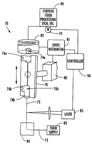
FIG. 8 illustrates one non-limiting example of an
apparatus 70 that can be used for forming an optical
microresonator having microcylinder resonators or ridges of
the present invention forming a resonant waveguide. The
apparatus 70 can use a laser "lathe" fabrication technique
with or without photoresist and etching steps. As
illustrated, an optical fiber 72 that is to form a
microcylinder is fed through first and second spaced ferrules
74a, 74b, which are supported by an upper and lower clamp 76a,
76b on a support member 78. The ferrules 74a, 74b include
precision fiber guides through which optical fiber passes,
such as drawn by a drive mechanism 79, which includes an
appropriate drive motor. The ferrules are typically formed
from ceramic, similar to optical fiber connector ferrules.
The upper clamp 76a can be designed to allow the ferrule 74a
holding the fiber 76 to rotate with the fiber inside. The
lower clamp 76b can be operative such that the fiber rotates
within the ferrule, but the ferrule 74b does not rotate. The
support member 78 is positioned on an x, y, z stage 80. A
drive mechanism 81 engages and drives the x, y, z stage 80 and
is controlled by a controller 90. The stage 80 allows
longitudinal movement along the axial fiber direction. A
chuck and drive mechanism 82 connects to the upper ferrule
-25-
CA 02542093 2006-04-06
74a. The clamps and ferrule can be designed such that the
fiber can be positioned and rotated by the chuck and
translated longitudinally by the stage. Fiber can be drawn
from a fiber supply 83 through a photoresist 84, where the
fiber is coated. The laser 85 provides appropriate light
exposure of the coated fiber for further processing, such as
etching, in one non-limiting example, at a processing station
86. The fiber can be fixed to the upper ferrule 74a to allow
rotation and longitudinal translation in an accurate and
precise manner driving the laser writing step. Thus, fiber
can be drawn from supply 83, its movement stopped, then
precisely controlled while laser writing occurs to make a
pattern. It should be understood that the laser can be
operative for machining any ridges or grooves directly on the
fiber.
A non-limiting example of the type of fiber that can
be used as a microcylinder in the present invention is SMF28
or similar single-mode fiber coated in photoresist. A non-
limiting example of a laser source that can be used in the
present invention is a 364 nm laser.
Light can be analyzed that propagates in cylindrical
guiding structures, i.e., the resonators or ridges, as
described above, or in similarly designed microcylinder
resonators operative to form a resonant waveguide. An example
could be an infinite microcylinder of radius, r, and
refractive index, n1. The microcylinder can be immersed in a
medium of refractive index, n2. The coordinate system can be
chosen with a z-axis parallel to the microcylinder axis and a
y origin at the center of the microcylinder. A whispering
gallery type guided wave would be assumed to propagate just
inside the microcylinder boundary. This wave is undergoing a
continuous reflection from the index discontinuity at the
boundary. A simplifying approximation can be used to replace
the circular microcylinder geometry with an equivalent planar
-26-
CA 02542093 2006-04-06
c
geometry. Because the fields are confined to propagate along
the circular boundary, the components at a larger radius would
propagate proportionately farther. This is approximately
equivalent to a planar system with a refractive index that
varies linearly with the distance from the now planar
boundary. This technique can be used to analyze bends in
optical waveguides. The effective index for the planar
equivalent guide is:
n = nly/r, in the region just inside the
microcylinder (y<0); and
n = n2y/r, in the region just inside the
microcylinder (y>0).
A one dimensional beam propagation coating model
could be constructed to represent this effective index
profile. FIG. 9 shows the modeled results obtained for a
surrounding index of 1.0 (air) and 1.33 (water) outside a
120-micron diameter microcylinder with body index, n1, of
1.498. This E field structure exhibits several modes when the
surrounding index is 1Ø At a 1.33 index, the fields are
almost single mode and at a 1.40 index there is a clean single
mode. The mode for the 1.4 index, however, has some radiation
loss as evidenced by the pedestal out to 20 microns on the
field pattern outside the microcylinder. A surrounding index
of 1.35 to 1.4 is desirable for a 120-micron diameter fused
silica rod. The fields are confined to within approximately 3
microns of the surface inside the microcylinder and penetrate
less than 1 micron outside the surface. The fields in all
cases began as a Gaussian profile with an 8.3-micron mode
field diameter. In this model, they are propagated 2 mm or
about five times around the microcylinder.
An index transformation can be used to analyze the
microcylinder propagation and create resonant waveguides on
the cylindrical surface. Because the effective index is
directly proportional to the distance from the axis, r, a
-27-
CA 02542093 2006-04-06
higher effective index region is created by increasing r. A
resonator, i.e., ridge, formed on the microcylinder can become
a resonant waveguide even though the actual refractive index
of the material in the ridge is identical or substantially
similar to that of the microcylinder itself. This is in
contrast to a ridge on a planar structure where no low loss
guiding is produced unless the index of the ridge exceeds the
index of the underlying plane.
A parameter that is used to characterize the guiding
power of an optical waveguide is D=(nl-n2)/nl. For the ridge-
on-a-microcylinder guide, D=(rl-rz)/rl=h/r, where h is the ridge
height and r is the microcylinder radius. A typical value for
D is 0.01. This corresponds to a 0.6 micron high ridge on a
microcylinder with a 60 micron radius.
Ridge guiding with homogeneous material enables the
manufacture of high quality resonant waveguides. For example,
only a photoresist mask could be applied where a waveguide is
desired. The surrounding material could be etched to a depth
required for the desired index step. A laser could be used to
expose pertinent sections of the photoresist. No deposition,
etching or modification would be required at the waveguide.
This fabrication technique leaves the critical waveguiding
region protected by the photoresist and unmarred by any
processing. Furthermore, the precision (radius, circularity,
etc.) of the original microcylinder is preserved in this type
of process. As previously mentioned, many complex and
intricate patterns can be created using this laser "lathe"
process for writing on the photoresist.
The index transformation described above provides
the parameters of a transformed step index in the planar
waveguide created by a microcylinder wall. Planar waveguide
analysis techniques and the effective index method could be
applied to solve for a wave field distribution in the axial
(z) direction. A single mode operation for a slab waveguide
-28-
CA 02542093 2006-04-06
could follow the function D=~2/8h2n1z. In this case, h is the
width of the planar guide, which is the width of the ridge on
the microcylinder in one example of the present invention. If
a reasonable value of 5 microns is chosen for a ridge width,
the D value is D<0.0055 for a single mode operation. This
corresponds to a 0.33 micron ridge height on a 60 micron
diameter microcylinder.
This geometry could be a good compromise between
lateral confinement under a ridge and controllable ridge
height. This level of detail will depend, of course, on
actual device fabrication techniques and end-use design. A
computed result for a modeled ridge-guided wave on a
microcylinder is shown in FIG. 10 for a 120 micron diameter
microcylinder, immersed in water, with a 0.33 micron ridge of
width 5 microns.
In the present invention input-output coupling is
possible such as by using an optical source waveguide, e.g.
optical fiber, and optical exit waveguide, e.g., another
optical fiber, for example as shown in FIG. 5. This system is
an improvement over prior art coupling techniques using
microspheres, or one tapered optical fiber near a
microcylinder. The present invention provides an improved
optical microresonator coupling system having a resonant
waveguide on the microcylinder in which energy can be coupled
into and out of the microcylinder. Coupling occurs when the
fields from an optical source waveguide overlap the fields
from a microcylinder resonator forming the resonant waveguide.
This requires proximity between the guiding core of the
optical source waveguide and the guiding core of the
microresonator. The interaction length, or propagation
distance in both the source and microresonator waveguide over
which this proximity must be maintained, is an important
parameter in the coupling relationship. The amount of
-29-
CA 02542093 2006-04-06
i
coupling generally varies as the square of the interaction
length.
Coupler design and implementation can also use a
gradual transition from an unperturbed optical source
waveguide into the coupling region and back out again through
the optical exit waveguide. For example, FIG. 11 shows a
filter 90 using a microcylinder 91 of about 125 microns with a
Free Spectral Range (FSR) of about 4.2 nm. An optical fiber
92 is operative as the optical source waveguide and has a
transition 92a down to the core, which is placed close to the
microcylinder and its resonant waveguide. The filter
throughput at the optical fiber 93 operative as the optical
exit waveguide is shown at the lower portion and occurs at
another transition 93a down to its core. Light enters the
fiber transition 92a and is coupled onto the microresonator
and is output form the microcylinder through the transition
93a.
In one example of the present invention, a resonant
waveguide could be considered to be a single mode waveguide
with a field E2. The source could be considered to be a single
mode waveguide with field E1. The symmetric power coupling
between the two waveguides is c. The value of c can be
computed from the field patterns and the coupling perturbation
by the equation:
ke-'~ZZ -
1) ~_ _ N r0(E1,EZ)e-Kcal-a2>Z'dz'dxdy
Where N is a normalizing constant
2 ) N = f ( E, ~ E z )dxdy.
~ is bn/n for the perturbing index variation.
-30-
CA 02542093 2006-04-06
The effects of mode mismatch on microresonator
performance can also be analyzed, in accordance with the
present invention. For example, a microresonator guide (E2,
width 5 microns, D=0.005) can be considered as a perturbation
in the field of a ridge waveguide (E1). A beam propagation
analysis can be used with the kernel of equation 1 above as a
concentrated source in a single plane parallel to the z-axis.
No microresonator losses are introduced in this example. The
model mismatch loss between the microresonator mode and the
optical source mode can be considered the dominant loss. A
mode-to-mode overlap of 0.7 causes half the coupled power to
go back into the optical source guide and half to be lost in
radiation or non-propagation modes. A model calculation for
this arrangement was performed and the steady state field
patterns for the incident mode, transitioned field, and
resonator field are shown in FIG. 12.
The graph in FIG. 12 shows steady state field
patterns. The graph line indicative for the transmitted field
is plotted as absolute value, such that the negative central
field is positive. Although the transmitted field is large,
the content of the propagating mode is more than 20 dB below
the incident field. The correlation coefficient between the
input source mode and the normalized microresonator field mode
is 0.71. The formation of the field pattern in the source
guide is seen in the transient field pattern shown in FIG. 13.
The corresponding field build-up in the microresonator is
shown in the transient field pattern of FIG. 14.
These model results are a 50/50 split of the light
between scattered modes and the propagating mode. It does not
represent a 50% loss in the microresonator, but a 50/50 split
between losses and coupling. A 50/50 split can be a target
for a loss to coupling ratio.
When using the microcylinders as described above,
the microcylinders may exhibit multiple passbands separated by
-31-
CA 02542093 2006-04-06
a
the free spectral range, a frequency interval equal to the
reciprocal of the transit time around the microcylinder.
Achieving a large free spectral range (FSR) may require a
small microcylinder.
As shown in FIG. 15, the zone of contact between the
microcylinder 95 (of about 10 microns) and the optical source
waveguide 96 and optical exit waveguide 97 are very short for
a small microcylinder 95. A 50 micron diameter microcylinder,
for example, could provide a contact length of less than 20
microns. Because the power coupling coefficient varies as the
square of the coupling length, this short coupling could limit
the use of the microresonator in some applications. The
multiple passband, FSR and the passband shape of a filter
based on a single microresonator could affect performance. A
single microresonator has a Lorentzian band shape, which falls
off as the first power of the frequency offset from the band
center. This is a slow drop for most applications.
Coupling and FSR can raise other issues. FIG. 16
illustrates coupled optical microresonators as microcylinders,
each having a resonant waveguide. Multiple microresonators
are coupled to an optical source waveguide and each other.
This is extendable to many microresonators. In FIG. 16, five
microcylinders 100a-a form a coupled waveguide microresonator
structure 101. In one non-limiting example, the structure 101
is a pyramid configuration. Three contacts 102a, 102b, 102c
are positioned at the optical exit waveguide 104. Two
contacts 102d, 102e are positioned at an optical source
waveguide 106. Because the microresonators are mutually
coupled, the coupled fields add coherently. Therefore, the
three contacts provide a nine-fold increase in coupled power.
This complex structure, however, does not always maintain the
proper phase relationship between all the coupling points
(seven in this example).
-32-
CA 02542093 2006-04-06
In accordance with the present invention, a coaxial
microcylinder to optical source waveguide coupling can be
established. Some of the phasing and contact spacing problems
of the structure in FIG. 16 can be alleviated by placing
coupled microcylinders concentrically on the same
microcylinder. But contact with multiple microresonators
requires that the microcylinder axis lie parallel to the
optical source waveguide axis. Coupling from an optical
source waveguide into a microresonator requires a coupling
element that changes the direction of propagation by 90
degrees (or any angle required to direct the light from the
source guide to the resonator guide when the axes are not
parallel) .
A coupling element, for example, a diffraction
grating or similar structure, for example, a dielectric line
structure as shown in FIG. 17, is one structure possible for
achieving this coupling. The coupling elements can couple
between waveguide modes and couple from optical waveguides to
resonators or ridges forming the resonant waveguide.
FIG. 17 shows an optical source waveguide 110
contacting the top of a series of ridges 112 forming a
resonator waveguide on a microcylinder 114. The angled series
of lines, forming the coupling element, for example a
diffraction grating 116, dielectric line, etched bump, notch,
groove or other structure is operative with the resonant
waveguide. In some aspects it is directly formed on the ridge
and spaced an integral number of wavelengths apart in contact
with the optical source guide. The coupling element could be
directly on or between the ridges. The resonators or ridges
forming the resonant waveguide may be mutually coupled by
proximity or by coupling structures overlaid on them. The
coupling length of this structure is not limited by the
microcylinder geometry and coupling lengths are limited only
by the precision required to maintain precise spacing and
-33-
CA 02542093 2006-04-06
phase relationships over the structure. If the waveguide
resonators or ridges are spaced sufficiently far apart, there
will be no mutual coupling and each acts independently. The
power coupled from the optical source waveguide varies in
direct proportion to the number of resonant waveguides in
contact with the optical source waveguide. If there is strong
coupling, the coupled power varies as the square of the number
of resonant waveguides in contact.
It is possible that a ridge forming a resonant
waveguide would not have to be used. If the grating contact
zone is long enough, a broad wavefront, e.9., a one
dimensional plane wave, propagates around the microcylinder.
Such a wide structure can be designed to have low diffraction
losses and no waveguiding is needed. The wide contact,
unguided resonator structure shown in FIG. 18 is an example.
For this geometry, the coupling is frequency
selective because the direction of the coupled wave steers
with wavelength. The frequency selectivity of this mechanism
is determined by the axial length of the coupling region in
wavelengths. The free spectral range is determined by the
circumference of the microresonator in wavelengths. When the
coupling length is large,~the circumference of the
microcylinder and the resolution of the coupling is sufficient
to select a single passband from the micro resonator and
reject the undesired spectral bands that are one or more free
spectral ranges away. This structure solves the problem of
achieving sufficient coupling length for good strength of
coupling and simultaneously solves the problem of multiple
passbands in the microresonators.
Another variation on the basic optical
microresonator as described is the array shown in FIG. 19.
The resonant waveguides are a continuous spiral, instead of
parallel bands or ridges. The turns of the spiral may be
coupled or uncoupled. This coupling can be controlled by the
-34-
CA 02542093 2006-04-06
1
choice of width and spacing of the turns or by other coupling
structures. In this example, the optical source waveguide 200
couples to a resonant spiral waveguide 202, and that guide
couples to a second spiral 204, both formed on respective
microcylinders 202a, 204a. A coupling element 206, for
example a diffraction grating, together with a chosen spiral
turn spacing, can be chosen to meet the desired phase matching
conditions between the optical source guide and the spiral
slow wave structure. The coupling element could be a
diffraction grating, etched bump, notches, dielectric lines,
or other structure.
The present invention improves upon the prior art
optical microresonators such as the published '730 patent
application. The present invention can include a resonant
waveguide having its ridges forming grooves such that ridges
are aligned in a predetermined manner to impart a desired
polarization, which can also be accomplished through
application of a coating in another aspect of the present
invention. The coating can also be advantageous for waveguide
slowing and polarization effects. The coupling of ridges with
a predetermined groove depth (height), spacing and angle
relative to the microcylinder can form a slow wave structure
and affect the waveguide coupled resonator and the coupling
mode with another optical source guide. The present invention
of course allows a multiple contact coupled structure as in
the example of FIG. 16 such that filters can be coupled
together.
It is possible that resonant waveguides as ridges
(and accompanying grooves) do not have to be formed on a
microcylinder to form a resonant waveguide and optical
microcylinder and, in the present invention, a "stripe" of
optical energy can possibly be placed around the microcylinder
such that the width of the strip of light going around the
microcylinder is not spread and is instead columnated as long
-35-
CA 02542093 2006-04-06
as it is not small relative to the order of the wavelength.
It is possible to obtain zero birefringence. FIG. 9, for
example, shows a modeled whispering gallery mode on a
microcylinder. Thus, it is possible that a resonant waveguide
using ridges may not be necessary on a microcylinder if a wide
stripe of light passes around the optical fiber without
spreading. It would be a function of the width of what is
being coupled into and the distance around the waveguide
relative to an angular spread of optical energy. For example,
a large diameter microcylinder with a narrow excitation would
not be advantageous because the optical energy would defract
as it goes around. It is not dominated by diffraction losses.
The present invention allows a microcylinder resonator and a
stripe that is wide enough to achieve low enough defraction
losses. This is a function of the engineering parameters of
the design. A coating would be even more advantageous.
There are advantageous positioning issues because it
is not necessary to position the optical source waveguide
within two microns of a five micron wide resonant waveguide
formed on the microcylinder. Thus, it is not critical where
the mode or touching is because it will be operable.
It is also possible to have a tapered optical fiber
that may or may not include a resonant waveguide as a ridge
and it can be slid back and forth relative to an optical
source waveguide for frequency tuning and selection. It
should be understood that some of these systems and devices as
described are polarization dependent and it is desired in some
cases to have polarization independence. In accordance with
the present invention, a coating or layer can be applied to
the microcylinder to produce a birefringence and bring two
polarizations in tune and alignment such that both
polarizations are the same within a given wavelength range.
The coating could be applied over ridges or other resonators
forming the resonant waveguide.
-36-
CA 02542093 2006-04-06
s
It should be understood that when using an optical
fiber, a user generally does not have control over the
polarization. It is possible that the ridges or other
resonator structure forming a resonant waveguide on the
microcylinder as described before, could be made of the right
index material and have the right thickness, and thus contain
a polarization independent property. As a result, there are a
set of parameters operable with the resonators, e.g. ridges,
that have the right thickness and right refractive index
material, and as a result the polarization independence is
established.
In some examples, a ridge by itself with a
refractive index the same as the underlying microcylinder
material would form a desired resonant waveguide. It is
possible to form a resonant waveguide out of higher index
material with the proper thickness to set a desired waveguide
property. For example, a coating could cause some polarized
lights to propagate faster and establish a birefringence. In
some instances, a coating alone over the microcylinder not
only could produce the desired resonator structure, but also
produce the polarization effect and bring polarization states
into degenerancy.
FIGS. 20 and 21 show the EMP model frequency
response of a respective 10 micron silica microcylinder and a
30 micron silica microcylinder with the axial and radial pole
modes shown and remaining separated for all diameters.
FIG. 22 shows a non-limiting model for a 9.5 micron
cylinder 200 with a 0.4 micron polymer coating 202 and the
optical source guide 204 adjacent within a testing chamber
206.
FIG. 23 shows the EMP model frequency response of
the 9.5 micron silica cylinder coated with a 0.4 micron
polymer shown in FIG. 22 and having an index of 1.55 and
-37-
CA 02542093 2006-04-06
showing the axial polarization and radial polarization and
showing a good matching of nodes.
FIG. 24 shows a finite difference time domain model
with the insertion loss of one optical microresonator as a
drop filter and shown next to and adjacent the optical source
guide as an optical fiber with the optical source waveguide
(in) and optical exit waveguide (out).
FIG. 25A shows two uncoupled micro resonators 220,
222 as a drop filter 224 and the In and Out positions of the
optical source guide 226. FIG. 25B shows the finite different
time domain model using the structure shown in FIG. 25A.
FIGS. 26, 27 and 28 show the response and the filter
transform function as a function of the wavelength for
respective 300, 400 and 500 nanometer thickness layers with a
film index of 1.55 and showing the source throughport and
waveguide output.
FIGS. 29, 30 and 31 show a response for respective
300, 400 and 500 nanometer coatings of a 1.50 film index and
showing the source throughport and waveguide output.
The coating as used in the present invention could
be accomplished by dip coating in a solvent until the solvent
dries, leaving the coating over the microcylinder. This is
similar to spraying on a varnish, where the solvent evaporates
and is left over as the coating after drying. This can be
accomplished in a controlled manner in the apparatus of FIG.
8. It could also be accomplished before or subsequent to any
ultraviolet step in the laser. The circumferential coating
could be formed from a polymer, such as a plastic as described
before, or a glass. The coating could range in one non-
limiting example from about 0.2 to about 1.0 micron thickness
on a microcylinder about 8.0 to about 150 microns diameter.
The film index could range in one non-limiting example from
about 1.4 to about 1.6.
-38-