Note: Descriptions are shown in the official language in which they were submitted.
CA 02542819 2006-03-15
_I_
DESCRIPTION
METALLIC THIN FILM CHIP PRODUCING METHOD AND
METALLIC THIN FILM CHIP PRODUCING APPARATUS
TECHNICAL FIELD
The present invention relates to a metallic thin film chip
producing method and a metallic thin film chip producing
apparatus.
BACKGROUND ART
In a conventionally adopted surface plasmon resonance
(SPR), mutual interaction of ligand and analite that are fixed on
a gold thin film of a gold thin film chip is optically observed. In
the SPR, how the mutual interaction of ligand forrczed on the
gold thin film and analite coupled to Iigand varies is optically
observed. It is general that the gold thin film on the gold thin
film chip is formed by vapor deposition.
Note that, SPC Electronics Corporation mentions a high
frequency induction heater, which heats metal, on its website
column alntroduction of High Frequency Induction Heater'°
([online], [searched on May I6, 2005], Internet URL:
http: / /www. spc. jp/ heating/tec.002.htm).
CA 02542819 2006-03-15
-2-
l;'urther, Japanese Unexamined Patent Publication No.
254904/2003 (Tokukai 2003-254904){Publication date:
September 10, 2003), Japanese Unexamined Patent Publication
No. 161694/2003 (Tokukai 2003-1.61694){Publication date:
June 6, 2003), Japanese Unexamined Patent Publication No.
75447/2003 (Tokukai 2003-75447)(Publication date: March 12,
2003), Japanese Unexamined Patent Publication No.
257720/2002 (Tokukai 2002-257720)(Publication date:
September 11, 2002), Japanese Unexamined Patent Publication
No. 6834/1999 (Tokukaihei 11-6834)(Publication date: January
12, 1999), or Japanese Unexamined Patent Publication No.
267$34/ 1998 (Tolaikaihei 10-267834)(Publication date: October
9, 1998) discloses a production method of a surface plasmon
resonance sensor chip.
However, a gold thin film formed by vapor deposition has
an excessively uneven surface. Particularly, in the SPR, even
when ligand is fixed in accordance with unevenness of the gold
thin film surface on which the ligand is to be fixed, it may be
impossible to obtain highly reproducible data, so that this
hinders the study on this held.
~rther, in order to form a gold thin film having a flatter
surface, the deposition method itself is improved (e.g.,
sputtering or a similar method is adopted). However, it takes
cost to improve the vapor deposition method. This results in
such a problem that the price of each gold thin film becomes far
from a practical price.
DISCLOSURE OF INVENTION
The present invention was made in view of the foregoing
problems, and an object of the present invention is to provide a
metallic thin film chip producing apparatus and a metallic thin
film chip producing method whereby it is possible to flatten an
CA 02542819 2006-03-15
excessively uneven surface of a metallic thin film at lower cost.
In order to solve the foregoing problems, a metallic thin
film producing apparatus according to the present invention
flattens a surface of a metallic thin filnn formed on a first
insulating substrate, and the metallic thin film chip producing
apparatus includes: a placement table on which a metallic thin
film chip is placed; pressing means for causing a second
insulating substrate to sandwich and press the metallic thin
filxn of the metallic thin film chip, placed on the placement table,
in a vertical direction with respect to the surface of the metallic
thin film; and heating means for heating the metallic thin film
of the metallic thin film chip placed on the placement table.
Further, it is preferable to arrange the metallic thin film
chip producing apparatus so that the heating means includes
magnetic flux generation means for generating a magnetic flux
penetrating the metallic thin film of the metallic thin film chip
placed on the placement table, and the magnetic flux causes the
metallic thin film to be heated.
Further, it is preferable to arrange the metallic thin film
chip producing apparatus so that the heating means is a high
frequency induction heater which includes a coil serving as the
magnetic flux generation means.
According to the foregoing arrangement, the metallic thin
film of the metallic thin film chip placed on the placement table
and pressed is heated by the heating means. The heating means
generates the magnetic flux. In case where the heating means is
the high frequency induction heater which includes the coil, the
coil of the high frequency induction heater generates a magnetic
flux upon applying an alternating current. In the metallic thin
film chip producing apparatus according to the present
invention, the magnetic flux generated by the magnetic flux
generation means penetrates the metallic thin film of the
CA 02542819 2006-03-15
-4-
metallic thin film chip placed on the placement table. When the
magnetic flux penetrates the metallic thin film in this manner,
an eddy current is induced in the metallic thin film due to
electromagnetic induction. The metallic thin film is heated to its
fusing point or the vicinity of the fusing point by the eddy
current.
The surface of the metallic thin film heated to the fusing
point or the vicinity of the fusing point as described above
becomes soft. The metallic thin film is sandwiched and pressed
by the first insulating substrate and the second insulating
substrate, so that a surface profle of the second insulating
substrate {the surface is in contact with the metallic thin film)
is transcribed onto the surface of the metallic thin film.
As described above, it is possible to transcribe the surface
profile of the second insulating substrate onto the metallic thin
film of the metallic thin film chip. By using the second
insulating substrate which has a surface being in contact with
the metallic thin film so that roughness of the surface (surface
unevenness) is lower than the surface roughness of the metallic
thin film, it is possible to improve the surface roughness of the
metallic thin film.
Thus, the metallic thin film chip flattened by the metallic
thin film chip producing apparatus according to the present
invention can be more easily produced than a metallic thin film
chip produced by high level vapor deposition, and it takes less
cost to produce the metallic thin film chip according to the
present invention than the metallic thin film chip produced by
high level vapor deposition.
Further, in the metallic thin film chip producing
apparatus according to the present invention, it is possible to
heat the metallic thin film of the metallic thin film chip rapidly,
so that it is possible to realize the metallic thin film chip
CA 02542819 2006-03-15
-5-
producing apparatus which can be easily automated.
Further, it is preferable to arrange the metallic thin film
chip producing apparatus according to the present invention so
that the heating means heats the metallic thin film of the
metallic thin film chip by irradiation of a microwave.
Furthermore, it is preferable to arrange the metallic thin flm
chip producing apparatus according to the present invention so
that the heating means is a dielectric heater which includes
microwave generation means for generating the microwave
irradiated to the metallic thin film of the metallic thin film chip.
According to the foregoing arrangement, the microwave
generation means irradiates the microwave to the metallic thin
film of the metallic thin film chip. Thus, oscillation of free
electrons becomes active in the vicinity of the surface of the
metallic thin film. The metallic thin film is heated to its fusing
point or the vicinity of the fusing point, so that the metallic thin
film is likely to be semi-liquid. Further, the pressing means
presses the metallic thin film, so that it is possible to improve
the surface roughness of the metallic thin fzlm.
1t is preferable to arrange the metallic thin film chip
producing apparatus according to the present invention so that
each of the placement table and the pressing means is made of
a material whose dielectric loss is small.
On this account, even when the magnetic flux penetrates
the placement table or the pressing means, the eddy current is
not induced, so that neither the placement table nor the
pressing means is heated. Thus, in the metallic thin film chip
producing apparatus, it is possible to heat only the metallic thin
film, so that it is possible to prevent the placement table and
the pressing means from being heated, thereby preventing
deformation of the placement table and the pressing means.
Further, the heating means gives the following effect: in
CA 02542819 2006-03-15
-6-
case of heating the metallic thin film of the metallic thin film
chip by irradiating the microwave, each of the placement table
and the pressing means made of a material whose dielectric loss
is smell allows a larger quantity of the microwave to pass
therethrough, so that the placement table and the pressing
means are not heated by the microwave irradiation, and heat
conduction does not heat the first insulating substrate and the
second insulating substrate for transcription.
It is preferable to arrange the metallic thin film chip
producing apparatus according to the present invention so as to
include a chamber for sealing up the metallic thin film chip
placed on the placement table in vacuum ox in an inert gas
atmosphere.
On this account, it is possible to prevent oxidization of the
metallic thin film of the metallic thin film chip, so that it is
possible to prevent the surface quality of the metallic thin film
from being deteriorated.
It is preferable to arrange the metallic thin film chip
producing apparatus according to the present invention so as to
include a chamber for shutting the metallic thin film chip
placed on the placement table in a same atmosphere as a room
air.
According to the foregoing arrangement, it is possible to
prevent the oxidization of the surface of the metallic thin film
since the microwave has a reducing property. Thus, according
to the foregoing arrangement, it is possible to obtain such an
effect that a trouble such as deaeration or inert gas exchange
carried out in a room can be avoided unlike a case where there
is provided a chamber for sealing up the metallic thin film chip
in vacuum or an inert gas atmosphere.
Further, it is preferable to arrange the metallic thin film
chip producing apparatus according to the present invention so
CA 02542819 2006-03-15
-7-
as to include fixation means for fixing the metallic thin film of
the metallic thin film chip with the metallic thin film
sandwiched by the second insulating substrate.
On this account, it is possible to prevent the metallic thin
film chip axed the second insulating substrate from deviating
from each other.
It is preferable to arrange the metallic thin film chip
producing apparatus according to the present invention so that
each of the placement table and the pressing means has a
property which allows the microwave to pass therethrough.
According to the foregoing arrangement, each of the
placement table and the pressing means has a property which
allows the microwave to pass therethrough, so that a large
quantity of the microwave generated by the microwave
generation means passes through the placement table and the
pressing means and reaches the metallic thin film. As a result,
the heating efficiency of the metallic thin film is improved.
Further, it is preferable to arrange the metallic thin film
chip producing apparatus so that the metallic thin film is made
of gold.
On this account, in case where the metallic thin film chip
producing apparatus according to the present invention is used
to flatten the gold deposited film surface of the gold deposited
chip used to carry out detection in SPR, it is possible to provide
the gold deposited chip whose surface is favorably flattened at
low cost.
Further, it is preferable to arrange the metallic thin film
chip producing apparatus according to the present invention so
that the second insulating substrate has a surface which is in
contact with the metallic thin film so that roughness of the
surface is 1 nm or less.
On this account, it is possible to transcribe the second
CA 02542819 2006-03-15
_$_
insulating substrate's surface roughness profile of 1 nzn or less
onto the metallic thin film of the metallic thin film chip. When
the surface roughness of the metallic thin film is set to 1 nm or
less, it is possible to carry out reproducible measurement also
in SPR.
In order to solve the foregoing problems, a metallic thin
film chip producing method according to the present invention
is a method for flattening a surface of a metallic thin film
formed on a first insulating substrate, and the method includes
the steps of: (i) causing a second insulating substrate to
sandwich and press the metallic thin film in a vertical direction
with respect to the surface of the metallic thin film; and (ii)
heating the metallic thin film.
Further, it is preferable to arrange the metallic thin film
chip producing method according to the present invention so
that magnetic flux generation means generates a magnetic flux
penetrating the metallic thin film so as to heat the metallic thin
film in the step (ii).
In the steps (i) and (ii), the metallic thin film is heated to
its fusing point or the vicinity of the fusing point and the heated
metallic thin film is pressed, so that it is possible to transcribe
the surface profile of the second insulating substrate onto the
surface of the metallic thin film. By selecting the second
insulating substrate whose surface roughness is low, it is
possible to flatten the surface of the metallic thin film.
Further, it is preferable to arrange the metallic thin film
chip producing method according to the present invention so
that microwave generation means irradiates a microwave to the
metallic thin film so as to heat the metallic thin film in the step
(ii).
It is preferable to arrange the metallic thin film chip
producing method according to the present invention so that
CA 02542819 2006-03-15
-9-
the steps (i) and (ii) are carried out in vacuum or an inert gas
atmosphere ar in a same atmosphere as a room air.
On this account, it is possible to prevent oxidization of the
metallic thin film of the metallic thin film chip, so that it is
possible to prevent the surface of the metallic thin film from
being deteriorated.
Further, it is preferable to arrange the metallic thin film
chip producing method according to the present invention so
that the metallic thin film is formed by vapor deposition.
For a fuller understanding of the nature and advantages
of the invention, reference should be made to the ensuing
detailed description taken in conjunction with the
accompanying drawings.
BRIEF DESCRIPTION OF DRAWINGS
Fig. 1(a) is a cross sectional view schematically
illustrating a structure of a metallic thin film chip producing
apparatus according to the present invention. Fig. 1 (b) is a
cress sectional view schematically illustrating a structure of the
metallic thin film chip according to the present invention.
Fig. 2 is a surface roughness profile obtained by observing
a predetermined straight line of a surface of a gold deposited
film through AFM.
Fig. 3 is a surface roughness profile obtained by observing
a predetermined straight line of a flattening glass substrate's
surface, which is in contact with a surface of the metallic thin
film, through AFM.
Fig. 4 is a surface roughness profile obtained by observing
a predetermined straight line of a gold deposited film, which has
been flattened by the metallic thin film chip producing
apparatus according to the present invention, through AFM.
Fig. 5 is a surface roughness profile obtained by observing
CA 02542819 2006-03-15
- x0 -
a predetermined straight line of a gold deposited film, which has
not been flattened by the metallic thin film chip producing
apparatus according to the present invention, through AFM.
Fig. 6(a) is a surface roughness profile obtained by
observing a predetermined straight line of a gold deposited film,
which has been kept at 500°C for 10 hours, through AFM. Fig.
5{b) is a surface roughness profile obtained by obserrring a
predetermined straight line of a gold deposited film, which has
been kept at 500°C for 30 hours, through AFM.
Fig. 7 is a surface roughness profile obtained by observing
a surface of a gold deposited film, which has been experimented
at a frequency of 2.45 GHz, an oscillation output of 950 W, a
compressive Ioad of 39.2 N (compressive stress of 0.30 MPa), for
a microwave oscillation time of 5 minutes, through AFM.
Fig. 8 is a surface roughness profile obtained by observing
a surface of a gold deposited film, which has been experimented
at a frequency of 2.45 GHz, an oscillation output of 950 W, a
compressive load of 39.2 N (compressive stress of 0.30 MPa), for
a microwave oscillation time of 3 minutes, through AFM.
BEST MODE FOR CARRYING OUT THE INVENTION
The following will explain one embodiment of a nrzetallic
thin film chip producing apparatus according to the present
invention with reference to Figs. 1 through 6. Note that, the
present invention is not limited to this.
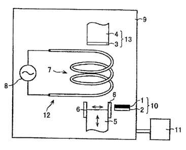
Figs. 1 (a) and 1 (b) are cross sectional views each of which
schematically illustrates the metallic thin film chip producing
apparatus according to the present invention. As illustrated in
Fig. 1(a), the metallic thin film chip producing apparatus
according to the present invention includes, in a vessel
(chamber} 9, pressing means 13 having an insulating substrate
3 and a pressing member 4, a chip placement table 5, and a
CA 02542819 2006-03-15
-I1-
heater (heating means) 12 having a coil 7 and a power source 8
for supplying an alternating current to the coil (magnetic flux
generation means) 7. On the vessel 9, a vacuum pump (air
exhaustion means) 11 for exhausting air from the vessel 9 is
provided.
In the metallic thin film chip producing apparatus, a
metallic thin film chip 10 obtained by forming a metallic thin
film 1 on an insulating substrate 2 (first insulating substrate) is
placed on the chip placement table 5. As illustrated in Fig. 1 (b),
the meta.J.lic thin film chip 10 placed on the chip placement
table 5 is sandwiched and pressed by the chip placement table
and the pressing means 13. At this time, the metallic thin film
1 of the metallic thin film chip 10 faces (is in contact with) the
insulating substrate 3 of the pressing means I3. Note that, the
metallic thin film 1 is sandwiched and pressed by the insulating
substrate 2 and the insulating substrate 3.
Further, the thus pressed metallic thin film 1 of the
metallic thin film chip 10 which is placed on the chip placement
table 5 is heated by the heater 12. The heater 12 is described as
follows. When an alternating current is supplied from the power
source 8, the coil 7 of the heater 12 generates a magnetic flux.
In the metallic thin film chip producing apparatus, the magnetic
flux generated by the coil 7 penetrates the metallic thin film I of
the metallic thin film chip 10 placed on the chip placement
table 5. When the magnetic flux penetrates the metallic thin
film 1 in this manner, an eddy current is induced in the
metallic thin film 1 due to magnetic induction. The metallic thin
film 1 is heated until the metallic thin film 1 reaches its fusing
point due to the eddy current.
A surface of the metallic thin film 1 heated to the fusing
point becomes soft. Further, the metallic thin film 1 is
sandwiched and pressed by the insulating substrate 2 anti the
CA 02542819 2006-03-15
_12_
insulating substrate 3, so that a surface profile of the insulating
substrate 3 which is in contact with the metailic thin filrrz 1 is
transcribed onto the surface of the metallic thin film I.
As described above, it is possible to transcribe the surface
profile of the insulating substrate 3 onto the metallic thin fi-iirr-1- w - ---
- w - w --- - w-- ---
of the metallic thin film chip 1Q. As the insulating substrate 3,
a substrate whose surface roughness (surface unevenness)
which is in contact with the metallic thin film 1 is lower than
surface roughness of the metallic thin film x, thereby improving
the surface roughness of the metallic thin film 1. In case where
the metallic thin film 1 is formed by vapor deposition, its
surface roughness is 5 nm, and the surface roughness of the
insulating substrate 3 may be arbitrarily set as long as it is
possible to improve the surface roughness of the metallic thin
film 1. For example, the surface roughness of the insulating
substrate 3 preferably ranges from 2 nm to 1 nm, more
preferably is 1 nm or lower. if it is possible to set the surface
roughness of the metallic thin film I to 1 nm or lower, it is
possible to realize reproducible measurement also in the SPR.
Further, it is possible to directly observe ligand, fixed on the
surface, through AFM (atom force microscope) and the like.
Note that, each of the insulating substrate 2 and the
insulating substrate 3 is made of insulating material. Thus,
even if the magnetic flux penetrates them, no eddy current is
induced, so that they are not heated. Therefore, in the metallic
thin film chip producing apparatus, it is possible to heat only
the metallic thin film 1, so that it is possible to prevent
deformation caused by heat of the insulating substrate 2 and
the insulating substrate 3.
Further, the vessel 9 is internally vacuumed by the
vacuum pump 11, thereby preventing the metallic thin film 1 of
the metallic thin film chip 10 from being deteriorated by
CA 02542819 2006-03-15
-13-
oxidization or the like. Also, an inert gas exchanging device for
infusing inert gas into the vessel 9 may be provided instead of
the vacuum pump 11. This can prevent the metallic thin film 1
of the metallic thin film chip 10 from being deteriorated.
Farther, a fixing member may be provided so that the
metallic thin film chip 10 and the insulating substrate 3 are not
deviated from each other. In the present embodiment, an.
example of the fixing member is a tape made of insulating
material or a similar member, but the fixing member is not
limited as long as the member is made of insulating material.
Further, the pressing member 13 is constituted of the pressing
member 4 and the insulating substrate 3 in the foregoing
description, but it may be so arranged that the insulating
substrate 3 is separately provided. In this case, the insulafiing
substrate 3 is placed on the chip placement table 5 while being
in closely contact with the metallic thin film chip 10 in advance,
and is pressed by the pressing member 4.
The respective members are described as follows.
The metallic thin film chip 10 is not particularly limited as
long as the chip is obtained by forming the metallic thin film 1,
produced by a conventional thin film production method, on the
insulating substrate 2. An example of the chip is an inexpensive
chip obtained by forming the metallic thin film 1 on the
insulating substrate 2 by vapor deposition or sputtering.
A material of each of the insulating substrate 2 and the
insulating substrate 3 is not particularly limited as long as the
material is an insulating material, but it is preferable to use a
material which is hardly softened by heat generated when the
coil 7 heats the metallic thin film 1. On this account, the
insulating substrate 2 and the insulating substrate 3 are not
deformed in pressing and heating the metallic thin film 1. Thus,
in flattening the surface of the metallic thin film l, it is possible
CA 02542819 2006-03-15
-14-
to exactly transcribe the surface unevenness of the insulating
substrate 2 or the insulating substrate 3 onto the surface of the
metallic thin film 1 of the metallic thin film chip 10, so that it is
possible to provide the metallic thin film chip producing
apparatus which can more evenly flatten the surface of the
metallic thin film.
Furthermore, in case of flattening the gold deposited film
used in the SPR, it is preferable to use a glass material as the
material of the insulating substrate 2 or the insulating
substrate 3.
A material of the pressing member 4 and the chip
placement table 5 is not particularly limited as long as each
material is an insulating material, but it is preferable to use
quartz glass or ceramic. This is based on the following reason.
The material is in contact with the insulating substrate 2 or the
insulating substrate 3, so that heat of the coil 7 raises
temperature of the insulating substrate 2 or the insulating
substrate 3, which may result in deformation of the insulating
substrate 2 or the insulating substrate 3 upon being pressed.
Particularly, as the material of the pressing member 4 and the
chip placement table 5, it is preferable to use a material whose
dielectric Ioss is small.
In the present embodiment, the metallic thin film 1 of the
metallic thin film chip 10 is heated to its fusing point of the
metallic thin flxn 1, but the arrangement of the present
invention is not limited to this. The metallic thin film 1 may be
heated at temperature which allows the metallic thin film 1 to
be softened. The temperature at which the metallic thin film 1 is
heated is influenced by a frequency of the alternating current
supplied from the power source 8 to the coil 7. As the frequency
of the alternating current is higher, the magnetic flux generated
by the coil 7 has higher density. The high density magnetic flux
CA 02542819 2006-03-15
-15-
penetrates the metallic thin film 1 of the metallic thin film chip
10, so that a high density eddy current occurs in the metallic
thin film 1. As a result, it is possible to heat the metallic thin
film 1 of the metallic thin film chip 10 to its fusing point or the
vicinity of the fusing point in a shorter time. The heating time
varies in relation to the temperature rise of the insulating
substrate 2 and the insulating substrate 3. As the heating time
is longer, the temperature further rises. Thus, it is preferable
that the heating time is shorter in consideration for deformation
of the insulating substrate 2 and the insulating substrate 3.
Therefore, it is preferable to set the frequency of the alternating
current to several KHz to several MHz in heating the metallic
thin film 1 in a short time. The heat generated in the metallic
thin flm 1 due to the eddy current vanes depending on
resistivity and permeability of the material of the metallic thin
film 1, so that it is possible to suitably set the frequency of the
alternating current in accordance with the material of the
metallic thin film 1 of the metallic thin film chip 10.
The heating time of the metallic thin film 1 of the metallic
thin film chip i 0, that is, the time in which the alternating
current is supplied to the coil 7 is influenced by the heating
temperature, so that it is possible to suitably set the heating
time in accordance with the material of the metallic thin film 1
of the metallic thin film chip 10.
As to a pressure load exerted by the pressing member 4
and the placement table 5, in case where the metallic thin film
1 is heated to its fusing point, it is possible to transcribe the
surface unevenness of the insulating substrate 3 onto the
metallic thin film 1 at about 0.1 to I0 MPa. Thus, the pressure
load ranging from 0.1 to 10 MPa is preferable. Note that, the
pressure load is not particularly limited as long as the pressure
Load does not damage the insulating substrate 2 and the
CA 02542819 2006-03-15
- 16-
insulating substrate 3. Under this condition, the pressure load
can be suitably set in accordance with the heating time and the
heating temperature of the metallic thin film Z, a metal type of
the metallic thin film 1, and an area size of the metallic thin
film surface of the metallic thin film chip 10.
Further, in the metallic thin film chip producing
apparatus illustrated in Fig. 1, the metallic thin film 1 of the
metallic thin film chip 10 placed on the pIacemcnt table 5 is
sandwiched and pressed in a vertical direction by the insulating
substrate 3, but the arrangement may be varied as long as the
metallic thin film 1 is sandwiched in a vertical direction with
respect to the surface of the metallic thin film 1. For example,
the metallic thin hlm chip producing apparatus may be
arranged so that: a direction in which the pressing member 4
exerts a pressure load is regarded as an upward direction, and
the metallic thin film is sandwiched in a horizontal direction (a
direction vertical to the upward direction).
Next, the following will explain an example of a production
method of the metallic thin film chip produced by the metallic
thin film chip producing apparatus according to the present
invention.
First, the metallic thin film chip 10 is prepared by forming
the metallic thin film 1 on the insulating substrate 2. Next, the
metallic thin film 1 of the metallic thin film chip 10 is
sandwiched and pressed by the insulating substrate 3 of the
pressing means from a vertically upward direction of the
metallic thin film 1 (step (l)).
Further, the coil 7 of the heating means causes the
magnetic flux to penetrate the metallic thin film 1 so as to heat
the metallic thin film 1 (step (ii)). At this time, the vessel 9 may
be internally vacuumed or an inert gas atmosphere is
introduced into the vessel 9. It is possible to generate the
CA 02542819 2006-03-15
-17-
magnetic flux by supplying the alternating current from the
power source 8 to the coil 7.
In the steps {l) and {ii), the metallic thin film 1 is heated to
its fusing point or the vicinity of the fusing point and the heated
metallic thin film 1 is pressed, thereby transcribing the surface
profile of the insulating substrate 3 onto the surface of the
metallic thin fihn 1. By selecting the insulating substrate 3
whose surface roughness is small, it is possible to flatten the
surface of the metallic thin film 1.
As described above, in the metallic thin film chip
producing apparatus according to the present invention and the
method according to the present invention for producing the
metallic thin film chip, the metallic thin film of the metallic thin
film chip obtained through simple and inexpensive vapor
deposition is heated by the coil in a short time while_baing___ _. ___ ____
___
pressed by the pressing means, so that it cost much less to
carry out these steps than the case where high level vapor
deposition is adopted. Moreover, it is possible to rapidly heat
the metallic thin film of the metallic thin film chip, so that it is
easy to autpmate the steps.
Fn case where the metallic thin film chip producing
apparatus according to the present invention and the method
according to the present invention for producing the metallic
thin film chip are applied particularly to the gold deposited chip
used in the SPR, it is possible to promptly obtain gold deposited
chips, each having a flat gold deposited fzlm surface, in large
quantity. Thus, it is possible to realize the low cost which allows
daily use of the gold deposited chip in the SPR, so that it is
possible to obtain reproducible data.
In the present invention, the heating means is not
particularly limited as long as it is possible to heat the metallic
thin film of the metallic thin film chip placed on the placement
CA 02542819 2006-03-15
- 18-
table. For example, the heating means may include microwave
generation means for generating a microwave. The heating
means heats the metallic thin film by irradiating the microwave
to the metallic thin film of the metallic thin film chip.
In case where the microwave is irradiated to a metallic
thin film whose thickness is relatively large (ranges from several
um to several mm), free electrons are more actively oscillated in
the vicinity of the surface of the metallic thin film, so that the
metallic thin film is heated. However, with the activation of the
free electron oscillation, a subsequent microwave cannot enter
the metaliic thin film, so that the microwave is likely to be
reflected by the surface of the metallic thin f lm (shielding effect).
Furthermore, when the oscillation of free electrons in the
vicinity of the surface is excessively active, some free electrons
fly out or jump to another substance (so-called electrical
discharge). Thus, the microwave irradiation has rarely been
used as a method for heating metal.
However, in east of a metallic thin film whose thickness is
extremely thin (nm order), such as the gold deposited chip,
which can be applied to the metallic thin film chip producing
apparatus of the present invention, the whole metallic thin film
can be regarded as the vicinity of the surface. Therefore, by
suitably adjusting a quantity of the supplied microwave to be
irradiated, it is possible to heat the metallic thin film to its
fusing point or the vicinity of the fusing point or until the
metallic thin film becomes semi-liquid.
Further, also in case of the metallic thin film whose
thickness is extremely thin, when the oscillation of free
electrons in the vicinity of the surface is excessively active,
some free electrons fly out or jump to another substance
(so-called electrical discharge). However, in the metallic thin
film chip producing apparatus of the present invention, the
CA 02542819 2006-03-15
9 _
pressing means causes the metallic thin film of the metallic thin
film chip placed on the placement table to be sandwiched and
pressed by the second insulating substrate in a direction
vertical to the surface of the metallic thin film. Thus, the
metallic thin film is closely sandwiched between the placement
table and the second insulating substrate. Therefore, free
electrons hardly fly out, so that it is possible to suppress the
electric discharge.
l~rther, it is preferable that each of the pressing means
and the replacement table is made of material whose dielectric
loss is small. In case where the dielectric loss is large, less
microwave passes through the material. In addition, irradiation
of the microwave heats the first insulating substrate and the
second insulating substrate for transcription due to heat
conduction. Thus, it is not preferable to use the material whose
dielectric loss is large. In case of using the material whose
dielectric lass is small, the pressing means and the placement
table are hardly heated by the microwave. Further, it is
preferable that the pressing means and the placement table
allow the microwave to pass therethrough. On this account, a
large part of the microwave generated by the microwave
generation means passes through the replacement table and the
pressing means, and then reaches the metallic thin film.
Therefore, it is possible to obtain such an effect that a heating
efficiency of the metallic thin film is improved.
An example of the material which allows the microwave to
pass therethrough includes a polymer material such as Pyrex
(registered trademark) glass, quartz glass, silicon resin,
polystyrene, polypropyrene, and fluorine. In case of using the
polymer material such as silicon resin, polystyrene,
polypropyrene, and fluorine, particularly in case of arranging
the metallic thin film chip producing apparatus so that the
CA 02542819 2006-03-15
-20-
metallic thin film is sandwiched from a horizontal direction (a
direction vertical to the upward direction), the material can be
favorably used.
Among them, it is preferable to use the pyrex (registered
trademark) glass since the pyrex (registered trademark) glass
allows a Iarge part of the microwave to pass therethrough and
its dielectric loss is small. The microwave is partially absorbed.
However, the dielectric loss of the pyrex (registered trademark)
glass is large, so that the irradiation of the microwave does not
raise the temperature. Therefore, a large part of the irradiated
microwave penetrates the pressing means and the placement
table each of which is made of pyrex (registered trademark)
glass, and reaches the surface of the metallic thin film. Note
that, the pyrex (registered trademark) glass is used as a vessel
used in a home electronic oven.
The dielectric loss of the quartz glass is smaller than that
of the pyrex (registered trademark) glass, and it is possible to
greatly suppress heat generation of the pressing means and the
placement table. Thus, it is more preferable to use the quartz
glass.
Further,, it is preferable to arrange the metallic thin film
chip producing apparatus according to the present invention so
as to include a chamber for shutting the metallic thin film chip
placed on the placement table in the same atmosphere as a
room air in case of heating the metallic thin film chip by
microwave irradiation.
In case of heating with the high frequency induction
heater, when the atmosphere has oxygen, the surface of the
metallic thin f lm is likely to be oxidized. Therefore, in case of
heating with the high frequency induction heater, it is
preferable to heat the metallic thin film in vacuum or an inert
gas. However, in case of heating through the microwave
CA 02542819 2006-03-15
_21_
irradiation, the microwave has a reducing property, so that it is
possible to heat in an atmosphere having oxygen. Therefore,
unlike the case where there is provided the chamber for
shutting the metallic thin film chip in vacuum or in an inert gas
atmosphere, it is possible to obtain such an effect that a trouble
such as deaeration or inert gas exchange carried out in a room
can be avoided. In this case, it is necessary to provide a
chamber for blocking the microwave so that the microwave does
not leak to the outside.
Further, in the microwave generation means, an
oscillation frequency, an oscillation output, or an oscillation
time of the microwave, or a pressure load exerted by the
pressing means can be suitably set in accordance with a size of
the metallic thin film, a type of the insulating material, a
placement point of the metallic thin film chip, or a spatial
structure of the chamber, etc. Qualitatively, in case of
increasing the oscillation frequency and the oscillation output
of the microwave, the oscillation time may be short.
For example, in case where the gold deposited chip is
applied as the metallic thin film chip, it is preferable to set the
oscillation frequency of the microwave to 2.45 to 100 GHz, and
it is preferable to set the oscillation output to 0.1 to 2 kW, and
it is preferable to set the oscillation time to 0.1 to LO minutes.
The oscillation frequency of 2.45 GHz is a frequency
whose maximum acceptable radiation value is free from any
limit as an ISM frequency band, and is open so as to be applied
to various industrial, scientific, medical, or home tools or
devices. Currently, an industrial oscillator whose frequency is
higher than that frequency is being developed. This oscillator is
referred to as agyrotron". An example of the oscillator is an
oscillator whose oscillation frequency is 28 GHz or an oscillator
whose oscillation frequency is 100 GHz. However, the oscillator
CA 02542819 2006-03-15
-22-
having such a high oscillation frequency is expensive, and it is
practical to adopt an oscillation frequency of 5.8 GHz or lower.
Thus, it is particularly preferable that the frequency of the
microwave applicable to the present invention ranges from 2.45
to 5.8 GHz.
Further, as will be described in Examples, when the
metallic thin film was heated at an oscillation output of 950 W,
the metallic thin film became semi-liquid by 5-minute
microwave irradiation. While, when 3-minute microwave
irradiation was carried out, the heating temperature was low.
When the oscillation output was decreased so as to be less than
950 W, it took some time (several ten minutes) for the metallic
thin film to be semi-liquid. Therefore, the microwave oscillation
output can be suitably set in accordance with a size of the
metallic thin film, a type of the insulating material, a placement
point of the metallic thin film chip, a spatial structure of the
chamber, etc., but it is preferable that the oscillation output
ranges from 0.1 to 2 kW. Note that, the oscillation output is an
oscillation output for a single metallic thin film chip. In case of
simultaneously heating several metallic thin film chips, it is
necessary to use an oscillation output obtained by multiplying
the foregoing oscillation output by the number of the metallic
thin film chips. Sortie industrial large scale oscillators can
realize 90 kW.
Further, the oscillation time can be suitably set in
accordance with the oscillation frequency or the oscillation
output of the microwave or other various conditions, but it is
preferable to set the oscillation time to 0.1 to 10 minutes.
In addition, the compressive load exerted by the pressing
means can be suitably set in accordance with the strength of
the metallic thin film. In case where the metallic thin film is so
soft that the metallic thin film is likely to be deformed, the
CA 02542819 2006-03-15
-23-
compressive load may be decreased. Further, in case where the
temperature is so low that the metallic thin film is hard to
deform, it is necessary to exert a higher compressive load. As
will be described in Examples, in case of heating through the
microwave irradiation, the metallic thin film was heated to the
vicinity of its fusing paint, so that the metallic thin film became
semi-liquid. Thus, by exerting the compressive load of 0.30 MPa,
the surface profile of the second insulating substrate was
transcribed. Therefore, in case where the metallic thin film is
completely fused as liquid, the compressive Load may be low.
However, in case of exerting the low compressive load after
changing the metallic thin film into liquid, the metal may leak
out. Further, in case of exerting a higher compressive load (in
case where the compressive load is higher than 10 MPa), the
second insulating substrate may be damaged. Therefore, it is
preferable that the compressive load exerted by the pressing
means ranges from 0.1 to 10 MPa.
More specifically, the microwave oscillation frequency is
set to 2.45 GHz, the oscillation output is set to 950 W, the
oscillation time is set to 5 minutes, and the compressive load
exerted by the pressing means is set to 0.30 MPa, thereby
flattening the gold deposited film of the gold deposited chip.
As described above, the metallic thin film is heated with
the microwave so as to keep a condition under which the
metallic thin film is likely to be deformed like a semi-liquid
condition, so that the pressing means can deform the surface of
the metallic thin film with a less compressive load (compressive
stress). Therefore, it is possible to more easily transcribe the
surface profile of the second insulating substrate onto the
surface of the metallic thin film.
Further, a circumstance in which the metallic thin film is
pressed and heated through the microwave irradiation heating
CA 02542819 2006-03-15
-24-
is not particularly limited. The microwave irradiation heating
may be carried out in a room air, an inert gas, or vacuum.
As described above, a metallic thin film chip producing
apparatus according to the present invention includes: a
placement table on which a metallic thin film chip is placed;
pressing means for causing a second insulating substrate to
sandwich aad press the metallic thin film of the metallic thin
film chip, placed on the placement table, in a vertical direction
with respect to the surface of the metallic thin film; and heating
means for heating the metallic thin film of the metallic thin film
chip placed on the placement table, wherein the heating means
includes magnetic flux generation means for generating a
magnetic flux penetrating the metallic thin film of the metallic
thin film chip placed on the placement table, and the magnetic
flux causes the metallic thin film to be heated, or the heating
means heats the metallic thin film of the metallic thin film chip
by irradiation of a microwave.
On this account, it is possible to heat the metallic thin
film to its fusing point or to the vicinity of the fusing point, so
that it is possible to easily transcribe the surface profile of the
second insulating substrate, being in contact with the metallic
thin film, onto the surface of the metallic thin film. Therefore,
the pressure exerted by the pressing means to the metallic thin
film allows improvement of the surface roughness of the
metallic thin film, thereby easily flattening the metallic thin film
chip.
The following Examples will detail preferable modes of the
present invention, but these Examples are mere references to
explain the present invention, so that the present invention is
riot limited to them. Person with ordinary skill in the art can
change, modify, and vary these Examples so as not to depart
from the scope of the present invention.
CA 02542819 2006-03-15
-25-
The following Example is given by illustrating a gold
deposited chip, obtained by depositing gold on a glass substrate
(corresponding to the insulating substrate 2) by vapor
deposition or sputtering, as a metallic thin film chip 10. The
gold deposited film corresponds to the metallic thin film 1.
[Example 1: Measurement of the thickness of the gold deposited
film]
In the present Example, the thickness of the gold
deposited film of the gold deposited chip was measured.
A surface of the gold deposited film of the gold deposited
chip was scratched with tweezers so that the glass substrate
was exposed, and the surface of the gold deposited film was
observed by an atom force microscope (AFM). Fig. 2 illustrates a
surface roughness profile obtained by observing a
predetermined straight line of the surface of the gold deposited
film by AFM. A point C on the surface of the gold deposited film
indicates a surface shape which had not been scratched by the
tweezers. Further, a point D indicates a surface shape in which
the insulating substrate 2 was exposed by scratching the
surface with the tweezers. Note that, in Fig. 2, x indicates a
direction of the predetermined straight line of the surface of the-
gold deposited film, and y indicates a vertical direction under
such condition that the surface of the gold deposited film in the
straight line was flat.
As indicated by the surface profile of Fig. 2, a distinct
difference between the point C and the point D of the surface of
the gold deposited film is found. A vertical distance between the
point C and the point D was measured. As a result of the
measurement, the vertical distance was about 50 nm. The point
D was the position in which the glass substrate was exposed, so
that the thickness of the gold deposited film was SO nm.
[Example 2: Measurement of surface roughness of a flattening
CA 02542819 2006-03-15
-2b-
glass substrate]
In the metallic thin film producing apparatus according to
the present invention, a flattening glass substrate used as the
insulating substrate 3 had a surface which was in contact with
the surface of the metallic thin film of the metallic thin film chip.
The surface roughness was measured.
In the flattening glass substrate, the surface which was in
contact with the surface of the metallic thin film 1 of the
metallic thin film chip 10 was observed by AFM. Fig. 3
illustrates a surface roughness profile obtained by observing a
predetermined straight line of the surface of the flattening glass
substrate which surface was in contact with the surface of the
metallic thin film 1. Note that, in Fig. 3, x indicates a direction
of the predetermined straight line of the flattening glass
substrate's surface which is in contact with the surface of the
metallic thin film 1, and z indicates a vertical direction under
such condition that the surface of the flattening glass substrate
was flat.
The surface roughness of Fig. 3 shows that a surface
roughness value of the flattening glass substrate is 1 nm. Note
that, the surface roughness value corresponds to a height
difference between a peak and a trough adjacent to each other
in the surface roughness profile. Thus, as the surface
roughness value is larger, the surface is more uneven.
[Example 3: Flattening of the gold deposited film by the metallic
thin film chip producing apparatus according to the present
invention]
The gold deposited film was flattened by using the metallic
thin film chip producing apparatus. As illustrated in Example 1,
the thickness of the gold deposited film was 50 nm. Further, an
area size of the gold deposited film was 3 mm x 5 mm = 15 mm2.
Note that, the flattening glass substrate used in Example 2 was
CA 02542819 2006-03-15
-27-
used as the insulating substrate 3.
First, a surface of the gold deposited film was observed
through AFM. Fig. 5 illustrates a surface roughness profile
obtained by observing a predetermined straight line of the
surface of the gold deposited film by AFM. Note that, in Fig. 5, x
indicates a direction of the predetermined straight line of a
surface on which gold was deposited, and z indicates a vertical
direction under such condition that the surface of the gold
deposited film in the straight line was flat. The surface
roughness profile of Fig. 5 shows that a surface roughness
value of the gold deposited film was 5 nm.
Further, in the present example, quartz glass materials
were used as the pressing member 4 and the chip placement
table 5 so as to flatten the gold deposited film. Note that, a
compressive load exerted by the pressing member 4 to the gold
deposited film was set to be a compressive stress of 1 MPa. The
inside of the vessel 9 was made vacuum, and an alternating
current of 1.7 KHz was supplied to the coil 7, and the gold
deposited film was heated for 30 seconds. Further, in the
present example, the gold deposited chip and the flattening
glass substrate were fixed with a scotch tape as a fixing member
so as not to be deviated from each other.
After heating, no change was found in the scotch tape,
and it was found that the scotch tape was not heated. Further,
the glass substrate of the gold deposited chip allowed direct
touch with hands. This means that only the gold deposited film
was heated by the coil 7. Also, this means that an eddy current
generated in the coil 7 resulted in a smaller total heat value of
the gold deposited film.
The surface of the gold deposited film subjected to the
foregoing treatment was observed by AFM. Each of Figs. 4{a)
and 4(b) illustrates a surface roughness profile obtained by
CA 02542819 2006-03-15
-28-
observing a predetermined straight line of the surface of the
gold deposited film by AFM. Note that, in Figs. 4(a) and 4(b), x
indicates a direction of a predetermined straight line of the
surface of the gold deposited film, and z indicates a vertical
direction under such condition that the gold deposited film was
flat.
As illustrated in Fig. 4(a), a surface roughness value of the
gold deposited film treated by the metallic thin film chip .
producing apparatus according to the present invention was 1
nm. The surface roughness value is equal to the surface
roughness value of the glass substrate used in Example 2. This
shows that the glass surface profile of the glass substrate was
transcribed onto the surface of the gold deposited film. Thus, it
was found that the surface profile of the gold deposited film was
transformed into a flat surface.
As illustrated in Fig. 4(b), an excessively uneven portion
was found in the surface of the gold deposited film. The surface
roughness value of the portion was 2 nm. This may be based on
the following reason: The compressive load exerted to the
surface of the gold deposited film of the gold deposited chip at
the time of the transcription was insufficient, so that the
surface of the flattening glass substrate was not sufficiently
filled with gold. Thus, the surface roughness can be improved
by increasing the compressive load.
[Comparative Example f J
The inventors of the present invention studied also a
method in which a gold deposited insulating substrate was
heated without being pressed and aggregation of gold deposited
particles on the insulating substrate was promoted so as to
flatten the uneven surface of the gold deposited film. When the
insulating substrate was heated at a temperature exceeding a
recrystallization temperature of gold (in. the vicinity of 200°C),
CA 02542819 2006-03-15
9_
the gold deposited particles grew through aggregation by
utilizing surface energy as a driving force, so that the gold
deposited film became flat. Ho~cvever, when the heating
temperature is high, the insulating substrate becomes soft. This
does not allow the gold deposited film to be flattened. Thus, it is
necessary to set the heating temperature to a temperature lower
than 500°C (softening paint of glass). Thus, the inventors
carried out a method in which the gold deposited film was
grown through aggregation in setting the heating temperature to
500°C.
In vacuum, the gold deposited chip was heated to 500°C
at a rate of 100°C/h. Further, after heating the gold deposited
chip, the gold deposited chip was kept at 500°C for 10 hours or
30 hours, and then the gold deposited chip was cooled to a
room temperature at a rate of 100°C/h.
A surface of the cold deposited film was observed by AFM.
Each of Figs. 6(a) and 6(b) illustrates a surface roughness
profile obtained by observing a predetermined straight line of
the surface of the gold deposited film through AFM. Note that,
in Figs. 5(a) and 6(b), x indicates a direction of the
predetermined straight line of the surface of the gold deposited
film, and z indicates a vertical direction under such condition
that the surface of the gold deposited film was flat. Fig. 6(a)
illustrates a surface roughness profile of the gold deposited film
kept at 500°C for 10 hours, and Fig. 6(b) illustrates a surface
roughness profile of the gold deposited film kept at 500°C for 30
minutes.
As illustrated in Figs. b(a) and 6(b), a surface roughness
value of an aggregated portion (a surface area of F in Fig. 6(a)
and a surface region of H in Fig. 6(b)) was 2 nm. While, a
surface roughness value of a portion which had not been
aggregated (a surface region of E in Fig. 5(a) and a surface
CA 02542819 2006-03-15
-30-
region of G in Fig. 6(b)) was 5 nm. As a result, it was found that
the gold deposited particles were aggregated when the gold
deposited film grew through aggregation by setting the heating
temperature to 500°C. In case where the gold deposited film was
kept for 30 hours, aggregation of the gold deposited particles
was further promoted than a case where the gold deposited film
was kept for 10 hours. However, also in the case where the gold
deposited film was kept for 30 hours, the aggregation locally
occurred, and some portions were not aggregated. It is expected
that the surface roughness of the gold deposited film will be
entirely even {the surface roughness value will be 2 nm) in case
where the gold deposited film is kept for longer time. However,
only the surface energy was used as a driving force to flatten
the uneven surface of the gold deposited film, so that a rate at
which the gold deposited particles were aggregated was low,
which resulted in higher cost.
[Example 4]
The metallic thin film chip producing apparatus of the
present invention was used to flatten the gold deposited film. An
area size of the gold deposited film was 13 mm x 10 mm ~ 130
~2.
The gold deposited filrrx was sandwiched by a flattening
glass substrate (second insulating substrate) whose surface
roughness was I nm or less, and a compressive load was
vertically exerted to the gold deposited film. Note that, as a
compressive-load poise {pressing means), a pyrex (registered
trademark) glass plate was used. Further, adjustment for
increasingJdecreasing the compressive load was carried out by
changing the number of pyrex {registered trademark] glass
plates.
In a room air, a microwave is irradiated to the gold
deposited film, thereby flattening the gold deposited film. The
CA 02542819 2006-03-15
-31-
microwave generation means had a frequency of 2.45 GHz and
an oscillation output of 950 W (commercial microwave oven).
Further, temperature adjustment for flattening the gold
deposited film was carried out by changing a microwave
oscillation time.
After flattening the gold deposited film, the surface of the
gold deposited film was observed by AFM.
In the present example, an experiment was carried out
under such condition that the compressive load was 39.2 N
(compressive stress was 0.30 MPa) and the microwave
oscillation time was 5 minutes. Under this condition, the
surface of the gold deposited film was observed by AFM. A
surface profile obtained by observing the surface of the gold
deposited film is illustrated in Fig. 7. As illustrated in Fig. 7,
the surface roughness of the gold deposited film was about 1
nm. It was found that the surface unevenness of the flattening
glass substrate was transcribed.
[Comparative Example 2j
The same operation as in Example 5 was carried out
except that the microwave oscillation time was 3 minutes, and
the surface of the gold deposited film was observed by AFM. As
a result, aggregation of the gold deposited particles was
recognized. This means that the gold deposited film was heated
to high temperature. A surface profile obtained by observing the
surface of the gold deposited film is illustrated in Fig. 8. As
illustrated in Fig. 8, the surface roughness of the gold deposited
film was greater than that of the gold deposited film which had
not been subjected to the microwave oscillation. Therefore, with
the microwave oscillation time of 3 minutes, the deposited
particles were aggregated, but an yield stress thereof was still
high, so that the gold deposited film was not sufficiently
deformed by the compressive stress of 0.30 Pa. This might
CA 02542819 2006-03-15
-32-
result in insufficient transcription of the surface unevenness of
the flattening glass substrate. Note that, the microwave
oscillation time was set to 20 minutes, but electric discharge
did not occur.
Based on Example 4 and Comparative Example 2, optimal
conditions of the heating and the compressive load in the
microwave heating are considered as follows.
Whether or not the surface unevenness of the flattening
glass substrate can be transcribed onto the surface of the gold
deposited film greatly depends on the yield stress of the gold
deposited film and the compressive stress which acts via the
flattening glass substrate. In case where the yield stress is low,
the surface unevenness of the flattening glass substrate can be
transcribed onto the surface of the gold deposited film even if
the compressive stress is low. However, in case where the yield
stress is high, the surface unevenness of the flattening glass
substrate cannot be transcribed onto the surface of the gold
deposited film unless the compressive stress is made
considerably high. Further, as the temperature of the gold
deposited filzrx is higher, the yield stress is lower. Particularly,
in case where the gold deposited film becomes semi-liquid, the
yield stress is extremely low.
In Example 4, the microwave was oscillated with an
output of 950 W for 5 minutes so as to flatten the gold
deposited film. The surface profile of the gold deposited flm is
illustrated in Fig. 7. In Example 4, the surface unevenness of
the flattening glass substrate was transcribed onto the gold
deposited film merely with the compressive stress of 0.30 Pa.
Thus, it is considered that the gold deposited film became
semi-liquid by heating with the microwave. While, in case where
the microwave was oscillated for 3 minutes as in Comparative
Example 2, as illustrated in Fig. 8, the surface unevenness of
CA 02542819 2006-03-15
-33-
the flattening glass substrate was not sufficiently transcribed
onto the gold deposited film with the compressive stress of 0.30
Pa. This may be based on the following reason: The temperature
of the gold deposited film was slightly Low, and the yield stress
was still high as described above. Thus, by raising the
compressive stress over the yield stress, it is possible to
improve the surface roughness of the gold deposited film.
While, in case where the oscillation output of the
microwave is raised, the gold deposited film may be semi-liquid
in short time. It is more preferable that the oscillation output is
higher in terms of a shorter processing time and mass
production of the gold deposited chips. Note that, as a
microwave oscillator for business use, there are various
commercial machines whose oscillation output is 1.5 kW or
further higher.
As described above, in order to transcribe the surface
unevenness of the flattening glass substrate onto the surface of
the gold deposited film, it is important to suitably set an
amount of supplied microwave (oscillation output and
oscillation time) and a compressive load (compressive stress).
The invention being thus described, it will be obvious that
the same may be varied in many ways. Such variations are not
to be regarded as a departure from the spirit and scope of the
invention, and all such modifications as would be obvious to
one skilled in the art are intended to be included within the
scope of the following claims.
INDUSTRIAL APPLICABILITY
The method according to the present invention for
producing the metallic thin f"ilm chip, the metallic thin film chip
producing apparatus according to the present invention, and
the metallic thin film according to the present invention are
CA 02542819 2006-03-15
-34-
applicable not only to a measuring device etc., using a chip
having a metallic thin film, which is based on SPR requiring the
flatness, but also to flattening pf the metallic thin film used as a
laser reflector.