Note: Descriptions are shown in the official language in which they were submitted.
CA 02542902 2006-04-19
WO 2005/039692 PCT/IB2004/003485
Method for generating an electrically contactable area on a doped
polymer and formed body produced by this method
Background of the Invention
The invention relates to a method for generating at least one electrically
contactable area on a polymer which is doped with a conductive substance,
wherein a contact material is applied onto the polymer, said contact material
having a lower specific resistance at 23°C than the polymer. The
invention
further concerns a formed body made of a polymer which is doped with a
conductive substance, which has at least one contactable area, within which a
contact material is applied onto the polymer, wherein said contact material
has
a lower specific resistance at 23°C than the polymer.
Electroconductive polymers are known and enjoy increasing popularity, in
particular also as material for producing electrodes for generating electric
fields
in various applications.
For example, an assembly for electrical arrangements is known from EP 0 307
007 B1, which comprises conductive components having different specific
resistances. A resistor made of a conductive polymer, i.e. a mixture of an
organic polymer and a conductive filler, which has a relatively high specific
resistance at 23 °C of 1 - 500.000 ohm x cm, is here provided with a
contact
layer consisting of a conductive material which has a specific resistance that
is
lower than the specific resistance of the resistor, i.e. a specific resistance
between 2,5 x 10⁻⁵ and 1 x 10⁻³ ohm x cm. The contact layer also consists of a
conductive polymer which is doped with a metal, e.g. silver, or a carbon-based
material, e.g. graphite. The contact layer is disposed onto the resistor in
the
form of band-like electrodes which interlock like fingers. Conductor rails are
provided as contacting elements, which consist of a stretched net made of
metal and which are folded around the contact layer and the electrodes formed
therefrom, respectively. The area at the edges of the electrodes act as
contact
CA 02542902 2006-04-19
WO 2005/039692 PCT/IB2004/003485
2
area. Although, with this solution, the input resistance of the resistance
layer is
reduced by application of a contact layer having lower specific resistance,
this
contact layer itself consists of a doped polymer and hence has still a
relatively
high input resistance as well. This is particularly true if demixing close to
the
surface occurs when the contact layer is injection-moulded. Furthermore, the
contact layer is here contacted via close-fitting conductor rails, i.e.
stretched
metal nets, and is thus not comparable to a dot-like contact. But there are
many
applications wherein dot-like contacting, e.g. via spring contacts, is
necessary
due to specific requirements or constructive conditions. But in this case, dot-
like
contacting of the disclosed contact layer would result in a burn-in of the
contacting elements to the contact points when very high voltages would be
applied.
Since metal ions are emitted from electrodes made of metal during electric
discharge, particularly in the field of biological applications, electrodes
made of
conductive synthetic material are advantageous compared to commonly used
metal electrodes. With the treatment of living cells, for example with
electroporation or electrofusion, metal ions emitted into the respective cell
suspension can either cause undesirable stimulation of the cells at lower
concentrations or, at higher concentrations, act toxic on the cells. For
instance,
when cuvettes made of aluminium are used a negative effect due to the release
of AI3+ ions could be demonstrated (Loomis-Hasselbee et al., Biochem J 1991,
277 (Pt 3), 883 - 885). Furthermore, if using cuvettes having electrodes made
of metal generation of metal hydroxides or complexes of metal ions with
biological macromolecules may occur (Stapulionis, Bioelectrochem Bioenerg
1999, 48(1 ), 249 - 254), what is often undesirable as well.
DE 102 08 188 A1 discloses containers with electrodes made of doped
polymers. The doped polymers are polymers which are blended with conductive
substances such as carbon fibres, graphite, carbon black (soot) or carbon
nanotubes. Although those doped polymers have lower conductivity compared
to intrinsically conductive polymers, it is a benefit that they are mouldable,
i.e.
that processing by the use of injection-moulding is possible. Thus, such doped
CA 02542902 2006-04-19
WO 2005/039692 PCT/IB2004/003485
3
polymers are variously useful and allow a cost-effective production of
electrodes by injection-moulding. But it is a problem with such electrodes
that
demixing occurs during the injection-moulding process so that the
concentration
of the conductive dope is relatively low at the surface of the electrodes.
Therefore, respective electrodes have a very high input resistance so that
very
high voltages have to be applied in order to achieve a sufficient current
flow.
But when usual dot-like contacting of these electrodes is used, for example
via
spring contacts, the contacts burn-in to the surface of the electrodes due to
the
high voltages applied so that the electrodes become unusable.
DE 101 16 211 A1 discloses a device for fusing living cells within an electric
field, wherein the electrodes are also made of a doped synthetic material,
i.e. a
plastic material which is blended with carbon. The electrodes are connected to
a voltage source via dot-like contact points and corresponding lead wires.
Thus,
also in this case it is a disadvantage that burn-in to the surface of plastic
electrodes would occur if voltages should be applied, which are higher than
those necessary for electrofusion. For example, to reach field strengths which
are sufficient for certain applications in electroporation significantly
higher
voltages have to be applied to the electrodes. Field strengths of 2 - 10 kV/cm
may be necessary, for instance, for the transfer of biologically active
molecules
into the nucleus of living cells. The voltage necessary to reach such field
strengths would also in this case result in a burn-in of the contact points if
the
known polymer electrodes are contacted dot-like.
Summary of the Invention
It is thus an object of the invention to overcome the existing deficiencies
and to
provide a method as identified above, which allows an effective reduction of
the
input resistance of the polymer within the contactable area in a simple and
cost-
effective manner. It is a further object of the invention to provide a formed
body
of the initially mentioned kind, which has a low input resistance, and which
can
be produced easily and cost-effectively.
CA 02542902 2006-04-19
WO 2005/039692 PCT/IB2004/003485
4
According to the invention this object is solved by a method as mentioned
above, wherein the contact material is applied onto the polymer so tightly
that
close contact between the contact material and the conductive substance is
achieved. Due to the tight application of the contact material, which has a
lower
specific resistance than the polymer, the input resistance of the doped
polymer
is effectively reduced, whereas the close contact between the contact material
and the polymer actually results in a merger of both components. Thus, an
intensive contact with the conductive dope of the polymer is achieved. In
order
to effectively reduce the input resistance, in particular for applications
which
require very high field strengths of 2 - 10 kV/cm between both electrodes, the
contact material has to be applied to the polymer so tightly that a connection
to
the dope of the polymer is established by the contact material, which is
sufficient to keep the temperature at the contact area between the polymer and
the contact material below the softening point of the doped polymer while
conducting electric current. Due to this measure it is possible to effectively
contact a polymer, which is doped with a conductive substance, dot-like within
the contactable area, i.e. for example via a wire or a spring contact, without
burn-in of the contacts to the surface of the polymer, even if high voltages
are
applied.
In an advantageous embodiment of the invention the contact material is applied
while being exposed to a temperature which is enhanced compared to room
temperature, preferably a temperature which is higher than the softening
temperature of the doped polymer, so as to establish a very close contact
between the contact material and the doped polymer. In the ideal case, both
materials may merge with each other. Additionally, impression or intrusion of
the contact material into the surface of the polymer is allowed hereby so that
the
contact with the dope of the polymer, i.e. the conductive material, can be
intensified so as to further reduce the input resistance.
If the contact material is applied under pressure the contact between the
contact material and the doped polymer can get much closer what results in a
CA 02542902 2006-04-19
WO 2005/039692 PCT/IB2004/003485
further advantageous reduction of the input resistance. In this case, the
contact
material may be preferably pressed onto the polymer.
In a particularly advantageous embidiment of the invention it is further
provided
5 that the surface of the polymer is at least partially enlarged by mechanical
and/or chemical treatment before the contact material is applied. Thereby, the
surface of the polymer can be roughened by mechanical invasion. This
measure facilitates the application of the contact material and additionally
ensures an intensified interlocking of both components.
The contact material should preferably have a very low specific resistance at
23°C, for example below 1 x 10⁻⁵ Ohm cm. The specific resistance should
be
preferably in the range from 1 x 10⁻⁶ to 2 x 10⁻⁶ Ohm cm.
In a further advantageous embodiment of the invention it is provided that the
contact material is a foil, preferably a metal foil, in particular a copper
foil, or a
foil made of an intrinsically conductive plastic material. By using a foil the
method according to the invention may be simplified, whereas additionally a
very thin and tight-fitting contact layer is generated. Copper may be a
particularly advantageous contact material since it has a very low specific
resistance of about 1,7 x 10⁻⁶ Ohm cm at 23°C. Furthermore, Copper is
easily
processable and inexpensive.
In a particular embodiment of the invention the polymer may be coated with a
contact material which comprises an intrinsically conductive plastic material,
whereby a very intensive contact between the polymer and the contact material
can be established in a simple and cost-effective manner. This embodiment is
further advantageous when metal cannot, or shall not, be used as contact
material.
In both embodiments described above the intrinsically conductive plastic
material may be, for example, polyaniline, polyacetylene, poly-para-phenylene,
CA 02542902 2006-04-19
WO 2005/039692 PCT/IB2004/003485
6
poly-para-phenylensulfide, polypyrroles, poly-thiophene or polypropylene, or
at
least based on one or several of these polymers.
Alternatively, the contact material may be a fluid or a suspension, preferably
suspended metal, particularly preferred a colloidal silver suspension. But it
is,
for instance, also possible to apply a drop of mercury onto the polymer. This
is a
very simple and economic method which could be advantageous with very
specific applications.
In a further alternative embodiment of the invention it is provided that the
contact material is a metal plate, preferably a copper plate, which is pressed
onto the polymer. In a special embodiment of the invention the metal plate is
heated before pressing, preferably to a temperature which is higher than the
softening temperature of the polymer, so as to allow impression of the metal
plate into the surface of the polymer in order to intensify the contact with
the
dope.
Before applying the contact material a carbon-based material, preferably at
least one graphite sheet, may be placed between the contact material and the
polymer, which effectively reduces the input resistance of the polymer.
In a particular embdiment of the method according to the invention the contact
material may be embossed onto the polymer under heat using an embossing
die, i.e. for example applied by hot-embossing. The contact material and at
least a part of the polymer may be thereby heated to a temperature which is
higher than the softening temperature of the polymer. The contact material is
subsequently applied onto the surface of the polymer under pressure using an
embossing die. Finally, the embossing die is lifted after cooling down to a
temperature which is lower than the softening temperature of the polymer.
While hot-embossing the contact material and/or at least one part of the
polymer and/or the embossing die may be heated to a temperature between
100 and 300°C. A pressure between 50 and 100 N/mm2 or between 100 and
500 N/mm2 may be applied to the embossing die. Alternatively, while
CA 02542902 2006-04-19
WO 2005/039692 PCT/IB2004/003485
7
embossing, at first a pressure between 50 and 100 N/mm2, preferably 70 and
90 N/mm2, and subsequently, during the cooling period, a pressure between
100 and 500 N/mm2, preferably 350 and 450 N/mm2, may be applied to the
embossing die. Embossing of the contact material under heat, for example hot-
s embossing, can take place, at least temporarily, in a vacuum or in a
nitrogen
atmosphere. In any case, hot-embossing is an effective and inexpensive
embodiment of the method according to the invention.
In an advantageous embodiment of the invention it is provided that the contact
material is applied onto the polymer by an adhesion-mediating layer which
preferably has a low specific resistance so as to improve the contact between
the contact material and the polymer. The adhesion-mediating layer may
advantageously be a conductive material, for example an electroconductive
adhesive or the like.
According to the invention the object of the invention is further solved by a
formed body as mentioned above, wherein the contact material is applied onto
the polymer so tightly that it is in close ,contact with the conductive
substance.
Such formed body has a significantly reduced input resistance and thus, can be
effectively contacted dot-like, i.e. via a wire or a spring contact, without
burn-in
of the contacts to the surface of the polymer when high voltages are applied.
The contact material has to be applied to the polymer so tightly that the
temperature at the contact area between the contact material and the polymer
is kept below the softening point of the doped polymer while conducting
electric
current. With the formed body according to the invention this result is
ensured
by the fact that the contact material has established a very close, i.e.
intensive,
connection to the dope of the polymer, which effectively reduces the input
resistance of the polymer.
In an advantageous embodiment of the invention the contact material may be a
metal, preferably copper, or an intrinsically conductive plastic material,
because
these materials have a low specific resistance and can be easily processed.
CA 02542902 2006-04-19
WO 2005/039692 PCT/IB2004/003485
The contact material should have a specific resistance at 23°C below 1
x 10-5
Ohm cm, preferably between 1 x 10⁻⁶ and 2 x 10⁻⁶ Ohm cm.
In order to further reduce the input resistance of the formed body according
to
the invention a carbon-based material, preferably a graphite sheet, or an
adhesion-mediating layer having a low specific resistance, may be disposed
between the polymer and the contact material, which each mediate an intensive
contact with the conductive dope of the polymer. In an advantageous
embodiment the adhesion-mediating layer may be a conductive material, for
example an electroconductive adhesive or the like.
The polymer is preferably doped with carbon fibres, graphite, carbon black
and/or carbon nanotubes, wherein the overall concentration of the dope in the
polymer is between 50 and 80 % w/w.
The polymer may be, for instance, polycarbonate, polyetheretherketone,
polypropylene, polyamide, preferably polyamide 6 or polyamide 66,
polyphenylensulfide or a mixture of these polymers, or at least based on one
or
several of these polymers.
The intrinsically conductive plastic material may be, for example,
polyaniline,
polyacetylene, poly-para-phenylene, poly-para-phenylensulfide, polypyrroles,
poly-thiophene or polypropylene, or at least based on one or several of these
polymers.
The formed body according to the invention preferably acts as an electrode or
a
similar member being necessary for conducting electric current. The formed
body may also be part of a cuvette or at least of one reaction chamber of a
multiwell plate, preferably in the form of an electrode, e.g. for
electroporation or
electrofusion of living cells, in particular for high throughput applications.
Table 1 shows characteristics of formed bodies according to the invention,
which are produced by the method according to the invention, compared to
CA 02542902 2006-04-19
WO 2005/039692 PCT/IB2004/003485
9
respective formed bodies without applied contact material. Electrodes made of
doped polymer are compared when contacted via spring contacts made of
brass. At first, electrodes without any contact material or intermediate layer
were testet. Using a voltage of 1000 V the spring contacts obviously burned-in
to the contact area of the electrodes. In a further experiment, the electrodes
were placed into an arrangement wherein contacting was not established
directly via the spring contacts but via a coper foil which was applied to the
contact area of the electrodes under low pressure. Also in this approach a
burn-
in of the copper foil to the contact area of the doped polymer could be
observed, even though at a lower level. In the various embodiments of the
formed bodies according to the invention, i.e. the electrodes produced by the
method according to the invention, no burn-in of the spring contacts or the
contact material to the contact area of the doped polymer could be observed
under same conditions. Thus, by tightly applying the respective contact
material
onto the doped polymer a burn-in of a contact element used can be certainly
avoided, even if a high voltage of 1000 V is applied.
Table 1: Avoiding of burn-in at the surface of formed bodies acting as
electrodes, which are made of doped polymer (Polyamide 6 with carbon fibres
and graphite)
Kind of Contact Direct Voltage applied;Burn-in;
Flown Char a Dama es on surface
Spring Contact (Brass) 1000 V; 5 mC Yes; significant
Copper Foil Adaptor 1000 V; 5 mC Yes; minor
about 20 mN/mm2
Copper Plates (about 1000 V; 5 mC No
2 N/mm')*
Copper Plates + Graphite1000 V; 5 mC No
about 2 N/mm2 **
55 wm Copper Foil, hot 1000 V; 5 mC No
embossed, 100 mm2
55 ~,m Copper Foil, 1000 V; 5 mC No
hot
embossed, 8 mm2
* Contact Area about 100 mm'
** Graphite: Density 1 g/cm3, 1 mm Thickness, 100 mm2 Contact Area on polymer
CA 02542902 2006-04-19
WO 2005/039692 PCT/IB2004/003485
Brief Description of the Drawings
The invention is described below in detail with reference to the drawings.
5 In the figures
Figure 1 is a cross-sectional view of a polymer cuvette which is equipped
with electrodes produced by the method according to the
invention,
Figure 2 shows a further embodiment of a polymer cuvette having
electrodes which are produced according to the invention,
Figure 3 shows bar diagrams of current strength and resistance, showing a
comparison of the conductivity of electrodes provided with contact
material and electrodes without contact material, wherein the
polymer cuvettes used are equipped with electrodes made of a
doped polymer (polyamid 6 with carbon fibres and graphite), and
wherein the contact material is a copper foil which is applied by
hot-embossing; thickness of the copper foil: 55 pm, gap length of
the cuvettes: 1,5 mm, volume of the electrolyte solution within the
cuvette: 100 pl, applied voltage: 1000 V Direct Voltage,
A: electrolyte solution having a specific conductivity of 17,02
mS/cm, n = 6
B: electrolyte solution having a specific conductivity of 17,02
mS/cm, n = 2,
Figure 4 shows bar diagrams of current strength and resistance of a
comparison of the conductivity of polymer cuvettes comprising
copper foils which are applied to different contact areas of the
doped polymer by the method according to the invention; broad =
100 mm2 and narrow = 18 mm2, gap length of the cuvettes = 1,5
mm, volume of the electrolyte solution - 100 pl, specific
CA 02542902 2006-04-19
WO 2005/039692 PCT/IB2004/003485
11
conductivity of the electrolyte solution = 12,75 mS/cm, thickness of
the copper foils = 55 pm, gray bars = 1000 V Direct Voltage, black
bars = 500 V Direct Voltage, n = 2,
Figure 5 shows bar diagrams of current strength and resistance of polymer
cuvettes equipped with electrodes made of doped polymer, which
are produced by the method according to the invention, and which
are contacted by copper plates pressed onto the electrodes with or
without intermediate layer, in comparison with spring contacts; gap
length of the polymer cuvettes = 1,5 mm, volume of the electrolyte
solution = 100 pl, specific conductivity of the electrolyte solution =
17,02 mS/cm, applied voltage = 1000 V Direct Voltage, n = 3,
a) spring contact made of brass,
b) solid copper plates which are pressed onto the electrodes with
an estimated pressure of 2 N/mm2,
c) copper plates pressed onto the electrodes with an estimated
pressure of 2 N/mm2, wherein graphite sheets having a density
of 1 g/cm3, a thickness of 1 mm, and a surFace area of about
100 mm2, are placed between the copper plates and the
polymer electrodes,
Figure 6 shows a perspective view of a cuvette comprising formed bodies
according to the invention, and
Figure 7 shows a perspective view of the cuvette according to figure 6
comprising a further embodiment of formed bodyies according to
the invention.
Description of various and preferred Embodiments of the Invention
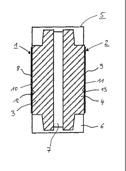
Figure 1 shows cross-section of two formed bodies 1, 2 according to the
invention, which, in this embodiment, act as electrodes 3, 4 of a cuvette 5.
The
cuvette 5 comprises a frame 6 which is made of a mouldable polymer and
CA 02542902 2006-04-19
WO 2005/039692 PCT/IB2004/003485
12
which comprises two oppositely arranged electrodes 3, 4 at the bottom. The
electrodes 3, 4 are also made of a mouldable polymer which is doped with
conductive substances, for example carbon fibres and/or graphite. The parallel
and oppositely arranged electrodes 3, 4 include a gap-like inner chamber 7
which serves for receiving a fluid, for example an electrolyte solution. An
electric
current flows through the fluid and the electrolyte solution, respectively, in
the
inner chamber 7 when an electric voltage is applied to the electrodes 3, 4.
Living cells may be suspended in the electrolyte solution and biologically
active
molecules, e.g. nucleic acids or proteins, which are solved in the electrolyte
solution, can be introduced into the cells by means of the electric current
flowing
through the inner chamber 7. In order to apply a voltage the electrodes 3, 4
have to be contacted on their outer sides 8, 9 by suitable contact elements,
for
example a spring contact. A contact material 10, 11 having a high conductivity
is tightly applied to both outer sides 8, 9 of the electrodes 3, 4 in order to
avoid
a burn-in of the contact elements, in particular if very high voltages are
applied.
In this embodiment, the contact material 10, 11 respectively covers the entire
respectively available contact area 12, 13 of the electrodes 3, 4. The contact
material 10, 11 can be, for example, a copper foil or a foil made of an
intrinsically conductive synthetic material. The contact material 10, 11
should
have a specific resistance at 23 °C below 1 x 10⁻⁵ ohm x cm.
Furthermore, the
contact material 10, 11 must be always tightly applied to the contact areas
12,
13 in order to effectively reduce the high input resistance of the electrodes
3, 4.
For this purpose, the contact material 10, 11 may be pressed, for example
under pressure, onto the contact areas 12, 13, preferably under heat, wherein
the temperature should be higher than the softening temperature of the
polymer. Alternatively, the contact material 10, 11 may be embossed onto the
contact areas 12, 13 by hot-embossing. In an alternative embodiment, the
contact material 10, 11 may also be applied to the contact areas 12, 13 by
means of an adhesion-mediating layer, e.g. by glueing. Due to the very tight
application of the contact material 10, 11 to the contact areas 12, 13 of the
electrodes 3, 4 a close, i.e. very intensive, contact between the contact
material
10, 11 and the dope of the electrodes 3, 4, i.e. the conductive material
within
the polymer, is achieved so that the contact material 10, 11 actually provides
a
CA 02542902 2006-04-19
WO 2005/039692 PCT/IB2004/003485
13
contact between the contact element (not shown), for example a spring contact,
and the conductive material within the electrodes 3, 4. In this manner, the
input
resistance of the electrodes 3, 4 is significantly reduced so that less heat
energy
is emitted at the contact areas 12, 13, i.e. at the contactable area. Due to
this
measure the temperature at the contact areas 12, 13 is kept below the melting
or softening point of the polymer forming the electrodes 3, 4 so that a burn-
in of
the contact element and the contact material is avoided. The formed bodies 1,
2
according to the invention, which are produced by the method according to the
invention, can thus also advantageously used in applications wherein high
voltages are used and a dot-like contacting shall, or must, be used.
Figure 2 shows a cross-sectional representation of a cuvette 14 which
substantially corresponds to the cuvette 5 according to figure 1. The
electrodes
20, 21 of the cuvette 14 are doped with a conductive substance as well, but
comprise no foil-like contact material at their contact areas 22, 23. In this
embodiment, metal plates 24, 25 are applied to the contact areas 22, 23. The
metal plates 24, 25 may consist, for example, of copper. Furthermore, the
metal
plates 24, 25 may be heated to a temperature which is higher than the
softening
temperature of the polymer so that they can impress or incise into the surface
of
the polymer. The metal plates 24, 25 are pressed with high pressure onto the
contact areas 22, 23 and vice-like loaded with a defined pressure by means of
pressure plates 26, 27 which respectively comprise thread regions 28, 29. In
this manner, the metal plates 24, 25 are pressed very tightly onto the contact
areas 22, 23. The input resistance of the electrodes 20, 21 is hereby
significantly reduced so that the metal plates 24, 25 can be contacted by
means
of dot-like contact elements, e.g. spring elements, without burn-in of the
contact
elements to the contact areas 22, 23 of the electrodes 20, 21.
Figure 3 shows conductivities of polymer cuvettes according to figure 1, which
are equipped with electrodes which comprise copper foils applied by hot-
embossing, compared to respective cuvettes having electrodes made of doped
polymer without contact material or embossed copper foil. In the bar charts
shown, it appears from the entire current flow and the measured total
resistance
CA 02542902 2006-04-19
WO 2005/039692 PCT/IB2004/003485
14
that due to the contact material applied to the electrodes the conductivity of
the
electrodes is enhanced. In all experiments an enhanced current flow and a
reduced total resistance could be measured when using contact material
(copper foil). Since the only difference between the compared cuvettes is the
contact material applied onto the contact areas of the electrodes these
experiments indicate that due to the use of contact material the input
resistance
of the electrodes could be reduced.
Figure 5 shows a comparison of cuvettes according to figure 2 with cuvettes
without integrally pressed copper plates, and with cuvettes comprising a
graphite layer which was inserted between the copper plates and the polymer
electrodes. On the one hand, it is herewith demonstrated that by pressing of
copper plates onto the electrodes made of doped polymer the resistance of the
electrodes can be significantly reduced. This fact is depicted in the bar
chart as
enhanced current flow and reduced resistance. On the other hand, the
resistance can be further reduced by insertion of a graphite layer between
copper plate and polymer electrode. It can be concluded herefrom that a closer
contact with the conductive material within the polymer can be established by
use of the flexible graphite layer.
Figure 6 shows a perspective view of a cuvette 30 which comprises a basic
body 31 and two formed bodies 32, 33 according to the invention. The formed
bodies 32, 33 are located in the narrowed regions at the bottom. The parallel
arranged formed bodies 32, 33 include a gap 34 which serves for receiving, for
example, a cell suspension. As can be seen with the formed body 33 a strip- or
band-like contact material 35 is applied onto the formed bodies 32, 33
according to the invention. Here, the contact material 35 may be, for example,
an embossed copper foil or the like. The formed bodies 32, 33 may be made of,
for instance, a polymer such as polyamid 6 or polyamid 66, which is doped with
carbon fibres and graphite. The formed bodies 32, 33 act as electrodes when
an electric voltage is applied to the contact material 35 so that an electric
field is
generated within the gap 34. By means of this electricl field biologically
active
CA 02542902 2006-04-19
WO 2005/039692 PCT/IB2004/003485
molecules may be transferred into cells by electroporation or cells may be
fused
by electrofusion.
Figure 7 shows a perspective representation of a cuvette 30 according to
figure
5 6, which comprises two electrodes 36, 37 at the bottom as well. Contrary to
the
formed body 32, 33 according to figure 6, with the electrodes 36, 37 a contact
material 38 completely covers the doped polymer. It is an advantage of this
embodiment that a larger area is provided for contacting. The contact material
38 may be, for example, an intrinsically conductive plastic material.
CA 02542902 2006-04-19
WO 2005/039692 PCT/IB2004/003485
16
List of References:
1 Formed body
2 Formed body
3 Electrode
4 Electrode
5 Cuvette
6 Frame
7 Inner chamber
8 Outer sides
9 Outer sides
10 Contact material
11 Contact material
12 Contact area
13 Contact area
14 Cuvette
Electrode
21 Electrode
22 Contact area
20 23 Contact area
24 Metal plate
Metal plate
26 Pressure plate
27 Pressure plate
25 28 Thread region
29 Thread region
Cuvette
31 Basic body
32 Formed body
30 33 Formed body
34 Gap
Contact material
36 Electrode
CA 02542902 2006-04-19
WO 2005/039692 PCT/IB2004/003485
17
37 Electrode
38 Contact material