Note: Descriptions are shown in the official language in which they were submitted.
CA 02542930 2006-04-13
WO 2005/039028 PCT/US2004/034194
METHOD AND APPARATUS FOR A WIRELESS POWER SUPPLY
FIELD OF THE INVENTION
The present invention is related to the retrieval
of radiated electrical energy. More specifically, the
present invention is related to the retrieval of radiated
electrical energy that is optimized for any given portion of
the RF spectrum using a plurality of taps.
BACKGROUND OF THE INVENTION
In the operation of the invention, ambient RF and
generated RF signals provide a source of potential energy
that can be gathered, stored and supplied to a multitude of
devices requiring electrical energy or that can restore
energy lost by a discharged source.
Traditional RF receiving devices utilize an antenna
to capture a narrow band of frequencies within the RF
spectrum, whereby the collection of RF frequencies is then
filtered, or tuned, to a specific frequency(s) for the
purposes of maximizing the signal being transmitted within
the chosen frequency(s). The potential energy contained in.
the signal is then used for its intended purpose, such as
audio, video or data processing. These RF receiving devices
have focused on maximizing selectivity of the frequency in
order to isolate and to be coherent without interference from
other sources.
CA 02542930 2006-04-13
WO 2005/039028 PCT/US2004/034194
-2-
SUMMARY OF THE INVENTION
The present invention pertains to an apparatus for
a wireless power supply. The apparatus comprises means for
receiving a range of RF radiation across a collection of
frequencies The apparatus comprises means for converting the
RF radiation across the collection of frequencies, preferably
at a same time into DC.
The present invention pertains to a method for a
wireless power supply. The method comprises the steps of
receiving a range of RF radiation across a collection of
frequencies. There is the step of converting the RF
radiation across the collection of frequencies, preferably at
a same time into DC.
BRIEF DESCRIPTION OF THE DRAWINGS
In the accompanying drawings, the preferred
embodiment of the invention and preferred methods of
practicing the invention are illustrated in which:
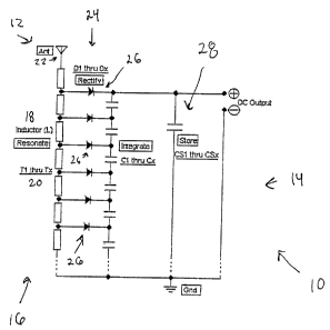
Figure 1 is a schematic representation of a
preferred embodiment of an apparatus of the present
invention.
Figure 2 is a schematic representation of a
preferred embodiment of an apparatus of the present invention
optimized for medium wave bandwidth RF energy retrieval,
collection and storage.
CA 02542930 2006-04-13
WO 2005/039028 PCT/US2004/034194
-3-
Figure 3 is a block diagram of the apparatus of the
present invention.
DETAILED DESCRIPTION
Referring now to the drawings wherein like
reference numerals refer to similar or identical parts
throughout the several views, and more specifically to figure
1 thereof, there is shown an apparatus 10 for a wireless
power supply. The apparatus 10 comprises means 12 for
receiving a range of RF radiation across a collection of
frequencies. The apparatus 10 comprises means 14 for
converting the RF radiation across the collection of
frequencies, preferably at a same time into DC.
Preferably, the converting means 14 includes an
absorbing mechanism 16 which is resonant for a desired band
of RF spectrum. The absorbing mechanism 16 preferably
includes an inductor 18 which is resonant for the desired
band of RF spectrum. Preferably, the converting means 14
includes a plurality of taps 20 placed at points along the
inductor 18 to access the RF energy.
The tap points preferably are calculated by
matching the inductor's 18 impedance to the desired band of
RF spectrum. Preferably, the receiving means 12 includes an
antenna 22. The converting means 14 preferably includes a
rectifying mechanism 24 which rectifies the RF energy and
converts it into DC voltage. Preferably, the rectifying
mechanism 24 includes a plurality of diodes 26 at each tap
CA 02542930 2006-04-13
WO 2005/039028 PCT/US2004/034194
-4-
point which rectifies the RF energy and converts it into DC
voltage.
The apparatus 10 preferably includes a storage
device 28 for storing the DC voltage. Preferably, the
antenna 22 impedance is matched 1:1 with the inductor 18
impedance. The RF spectrum preferably is between 60 Hz to 28
gigahertz.
The present invention pertains to a method for a
wireless power supply. The method comprises the steps of
receiving a range of RF radiation across a collection of
frequencies. There is the step of converting the RF
radiation across the collection of frequencies, preferably at
a same time into DC.
Preferably, the converting step includes the step
of absorbing the energy. The absorbing step preferably
includes the step of absorbing the energy with an inductor
18. Preferably, the converting step includes the step of
accessing the absorbing energy with a plurality of taps 20 on
the inductor 18. There is preferably the step of matching
the inductor's impedance to a desired RF range.
Preferably, the converting step includes the step
of rectifying energy available at each tap and converting it
into DC voltages. The rectifying step preferably includes
the step of rectifying the energy available at each tap and
converting it into DC voltages with diodes 26. Preferably,
the converting step includes the step of summing the DC
CA 02542930 2006-04-13
WO 2005/039028 PCT/US2004/034194
-5-
voltages. The summing step preferably includes the step of
adding the DC voltages among a series capacitor integrator.
Preferably, there is the step of storing the summed DC
voltages. There is preferably the step of using the stored
DC voltages.
A method and apparatus 10 for retrieval of radiated
electrical energy is described herein. The radiated energy
to be captured is being transmitted in the portion of the
electromagnetic spectrum sometimes referred to as RF, or
Radio Frequency. The primary purpose of the method and
apparatus 10 described herein, is to receive RF energy and
convert the energy into a usable form of power. The method
and apparatus 10 does not discern or interpret individual
signals or frequencies. It is designed to absorb and convert
signal, carrier and any associated interference for a chosen
band or range of frequencies into reusable power.
In contrast, to traditional RF receiving devices,
this methodology and apparatus 10 avoids selectivity. It has
the unique characteristic of accepting broad ranges of the RF
spectrum as a collection of frequencies. Each collected
range of frequencies is then rectified, or converted, as a
whole into a single voltage. Preferably, at the same time of
RF absorption, the resultant voltage is generated. The
apparatus 10 makes no attempt to tune for any specific
frequency or signal. Each voltage, which is gathered from a
given range of frequencies, is then added together and made
available to power a device directly, to be stored, or to
supply energy to a recharging apparatus.
CA 02542930 2006-04-13
WO 2005/039028 PCT/US2004/034194
-6-
The radiated electrical energy, to be utilized by
the circuit, can be in the form of a wide range of the RF
spectrum. Some examples of ambient RF sources can include,
but are not limited to: Very Zow Frequency-VZF
(Maritime/Aeronautical Mobile), Medium Frequency- MF (AM
Radio Broadcast), High Frequency- HF (Shortwave Radio
Broadcast), Very High Frequency- VHF (TV and FM Radio
Broadcast), Ultra High Frequency- UHF (TV, HDTV, PCS, WiFi)
and certain Microwave transmissions. In addition, the
apparatus 10 allows for the reception of dedicated RF
transmission that are generated and broadcast for the
specific purpose of transmitting power to the apparatus 10
for absorption, collection and utilization. In this case, it
is not necessary for the dedicated RF transmission to contain
a specific signal or data that needs to be interpreted for
ancillary purposes such as audio/video or data reception and
interpretation.
Using the technique described herein, one can
design and create an apparatus 10 that is optimized for any
given portion of the RF Spectrum. The necessary electrical
and magnetic characteristics of the apparatus 10 components
will vary depending on the chosen portion of the spectrum.
Because of this, it is impractical to create one single
apparatus 10 to cover the entire RF spectrum. However, it is
possible to create individual apparatus 10, each designed for
a given RF band, and combine both the apparatus 10, their
outputs for maximum power efficiency.
CA 02542930 2006-04-13
WO 2005/039028 PCT/US2004/034194
A portion of a selected RF frequency band is
intercepted by an antenna 22 placed in the field of emitted
energy. The antenna 22 receives energy, in accordance with
its design efficiency, and directs it into a system where it
is absorbed, rectified, summed and delivered for use or
storage.
RF Energy -> Antenna-->[Absorbed-Rectified->Integrated-Delivered]-Used
RF signals striking an antenna 22 are fed into an
inductor (L), which is resonant for the desired band of RF
spectrum. Note: In areas with a high concentration of RF
energy, there is no need to attach an antenna 22. The
absorbed RF energy, consisting of fundamental, harmonic,
inter-harmonic and standing waves is accessed via taps 20
(T1-Tx) on the inductor 18 which are placed at points along
the inductor 18. A key characteristic of this device is that
a capacitor-less front-end allows for the inductors' wide
bandwidth and maximum admittance of the incoming RF energy.
The tap points are calculated by matching the inductor 18
section's impedance to the desired RF range.
The resultant RF energy, available at each tap
point, is rectified by a device, such as diodes 26 (D1-Dx),
and converted into DC Voltages. The individual rectified
voltages are spread among a series capacitor integrator
consisting of capacitors (C1-Cx). This broadband approach
allows maximum energy to be spread among the series capacitor
stack.
CA 02542930 2006-04-13
WO 2005/039028 PCT/US2004/034194
_g_
The sum of the voltages available from C1-Cx is
stored in any storage device 28 such as a capacitor or group
of capacitors Cs (s1-sx) and made available for immediate
use, or to supply electronic devices) requiring intermittent
power. The electrical characteristics of the storage devices
or capacitors, the configuration and actual number of storage
devices is dependent on the voltage and power requirements of
the device the apparatus 10 is delivering power to. (See
Figure One)
Although not considered part of the apparatus 10,
the antenna 22 is an integral component of any practical
device utilizing the method and apparatus 10 described. The
key characteristics of the antenna 22 would be that it is
capable of wide band reception, optimized for the chosen
bandwidth, and takes into consideration the necessary
effective area to support the power requirements of the
target device.
Ideally, the antenna 22 impedance is matched 1:1
with the inductor 18 impedance of the apparatus 10.
2p Note: In areas with a high concentration of
RF energy, there is no need to attach an
antenna 22 to the apparatus 10.
Inductor 18:
The characteristics of the inductor 18 is dependent
on the chosen bandwidth of frequencies to be collected and
utilized. The ideal inductor 18 should be constructed so
CA 02542930 2006-04-13
WO 2005/039028 PCT/US2004/034194
-9-
that the mid point of total inductance would be resonant at
the center frequency of the chosen RF segment or spectrum.
Multiple taps 20 provide fundamental and inter
harmonic output voltages from the selected band segments of
radio frequency energy.
For example, a medium wave circuit (figure 2),
utilizing an antenna 22 impedance of 375 ohms, into an
inductive circuit with 375 ohms of reactance, with a center
frequency of 1.2 MHz would require an inductance of 100 uH.
The effective bandwidth would be approximately 2 MHz wide. (-
3 db down at each end of the band).
The inductor 18 can be calculated using the
following standard resonance formula (Formula 1):
L = (d squared times n squared) divided by (18 times d plus
40 times j)
Where
L = inductance in micro-henrys.
d = conductor diameter in inches.
j - conductor length in inches.
n = number of conductor iterations.
Using similar formulae, the required inductance can
be re-calculated for henrys, milli-henrys, pico-henrys and
nano-henrys. ie. VLF, LF, MW, HF, VHF, UHF and Microwave
frequency band segments.
CA 02542930 2006-04-13
WO 2005/039028 PCT/US2004/034194
-10-
Utilizing a capacitor-less front-end insures the
inductors' wide bandwidth, and maximum admittance to the
incoming RF energy.
Taps 20:
Taps 20 are to be constructed and placed at points
along the inductor 18. Each tap provides an individual
output voltage into the rectifying portion of the apparatus
10.
The number of taps 20 from the inductor 18 can be
calculated by the following formula (Formula 2):
Tn = Bw times pi
Where
Tn = Total number of taps.
Bw = Effective Bandwidth of inductor (in Megahertz).
Pi = 3.1416
The default position of each tap on the inductor 18
is equidistant along the inductor 18. Tap positions can also
be calculated for optimum output voltage. When calculating
the taps 20, one must take into consideration known
frequencies within the chosen band segment that contain
higher RF energies, And using a standard resonance inductance
formula (1) each individual tap can be calculated for the
required frequency and optimum voltage output.
CA 02542930 2006-04-13
WO 2005/039028 PCT/US2004/034194
-11-
Rectifiers:
The RF energy available at each tap is converted to
DC voltage via a rectifying device. The type of rectifying
device to be used is dependent on the chosen frequency band,
and includes crystal, germanium, silicon and any other types.
Integrator:
A voltage integrator is composed of capacitors C1
- Cx. The values of these capacitors are dependent on the
chosen frequency band, the unique characteristics of the
rectifiers and the load imposed by the Storage stage. The
reactance of this circuit varies greatly, even during normal
operation. However, one can use a standard formula for
capacitive reactance as a starting point for preliminary
calculations:
Xc = 1/ (2*pi*F*C)
Where
Xc= Capacitive reactance in ohms
C = Capacitance in Microfarads.
F = Frequency in Hertz.
Pi = 3.1416
Storage:
Storage components) are determined by the power
requirements of the attached device(s), and the available RF
energy absorbed by the inductor (L).
CA 02542930 2006-04-13
WO 2005/039028 PCT/US2004/034194
-12-
Using a Medium Wave example, a 2, 200 micro-farad electrolytic
capacitor is used as storage.
Sample Apparatus 10: Medium Wave (AM) Wireless Power
Supply
A device has been constructed, using the method
stated above, which uses the ambient (existing) AM Broadcast
band of the RF spectrum as its source of energy. The
device's primary purpose is to optimize the energy absorbed,
collected and converted to reusable power.
The size and characteristics of the antenna 22
required for the circuit to operate are not considered a
design requirement for the apparatus 10. The antenna 22
needed to obtain sufficient energy to charge a storage device
28 in a typical urban area with several AM radio stations,
would be similar to one used for a standard AM radio. In
areas where there is a higher concentration of RF energy, the
apparatus 10 itself, without an antenna 22, is sufficient to
develop stored power.
The inductor 18 is in the form of an air coil
comprised of enameled #28 gauge wire wound onto a 2" form.
The coil is a continuous tightly wound wire with taps 20
placed every twenty turns with a total of six taps 20
available (T1 - T6). The top of the coil is where the
antenna 22 is connected. The bottom of the coil is connected
to ground.
CA 02542930 2006-04-13
WO 2005/039028 PCT/US2004/034194
-13-
Germanium diodes (IN34A) (D1-D6) are connected to
each tap on the coil. The series capacitor integrator (C1-
C6) is constructed as illustrated with the C6 attached to
ground. C1-C6 are poly capacitors with a 0.068uF rating.
The power storage device 28 utilized in this sample apparatus
10, C7, is a 2200uF electrolytic capacitor.
Very wide band operation can be utilized by
coupling multiple instances of the Broadband Wireless Power
Supply together.
For Example:
A BWPS circuit designed and constructed (see design
considerations) for a Very Low Frequency wave segment (60 Hz
center frequency), can be coupled into another BWPS circuit
designed and constructed (see design considerations) for an
Ultra High Frequency wave segment (5 GHz center frequency).
The outputs of each individual circuit connect (via another
integrator circuit) into a common storage device 28 (i.e.,
capacitor) to "pool" collected and converted RF energy
together. This technique can be repeated for any or all
segments of the energy spectrum.
Although the invention has been described in detail
in the foregoing embodiments for the purpose of illustration,
it is to be understood that such detail is solely for that
purpose and that variations can be made therein by those
skilled in the art without departing from the 'spirit and
CA 02542930 2006-04-13
WO 2005/039028 PCT/US2004/034194
-14-
scope of the invention except as it may be described by the
following claims.