Note: Descriptions are shown in the official language in which they were submitted.
CA 02542983 2006-04-19
WO 2005/041425 PCT/US2004/034739
Full-Duplex Radio Frequency Echo Cancellation
Backaround
[0001] Radio frequency identification ("RFID") systems are
used in a plethora of commercial contexts requiring a unique
identification system for large numbers of items. Such contexts
include everything from department store inventory and check-out
systems to the tracking of military supplies to and from the
front lines. Similar in utility to bar code technology, RFID
systems are often preferred due to their increased range, lack of
a line of sight requirement between a tag and its reader and the
high multi-tag throughput of RFID readers {i.e., RFID readers may
read many tags in their large field of view at very high
transport speeds).
[0002] A problem that arises is that optimal performance of
RFID systems is often hampered by the reflection and coupling
which inevitably occur in RF transceivers, in which a significant
portion of the transmitted interrogation signal is reflected by
the antenna and objects in the environment into the receiving
portion of the transceiver. These problems are quantified in a
measure called the voltage standing wave ratio ("VSWR"), measured
as the non-transmitted {i.e. coupled or reflected from the
antenna or non-RFID objects in the environment) power over the
total transmitted power of the transceiver. A high VSWR
interferes with efficient transceiver performance and may even
result in a "blinding" or complete saturation of the receiver.
Transceivers designed to minimize vSWR are often unacceptable
because of their high cost in terms of size and power, especially
in the context of mobile devices.
Summiarv of the Invention
CA 02542983 2006-04-19
WO 2005/041425 PCT/US2004/034739
[0003] A system comprising a transmitter element creating an
interrogation signal and transmitting the interrogation signal
and a receiver element receiving a reflection signal of the
interrogation signal and combining the reflection signal and a
feedback signal to cancel at least a portion of radio frequency
echo signals in the reflection signal.
[000~~ A method, comprising the steps of receiving a
reflection signal, deriving a feedback signal from the reflection
signal by isolating an error component of the reflection signal
and combining the reflection signal and the feedback signal to
cancel at least a portion of radio frequency echo signals in the
reflection signal.
[0005 Furthermore, a method comprising the steps of
demodulating a reflection signal into an in-phase signal and a
quadrature signal, filtering the in-phase signal to isolate an
in-phase error signal, filtering the quadrature signal to isolate
a quadrature error signal, modulating the in-phase error signal
and the quadrature error signal to create a feedback signal and.
combining the reflection signal and the feedback signal to cancel
at least a portion of radio frequency echo signals in the
reflection signal.
[0006 In addition, a system, comprising a demodulator to
demodulate a reflection signal into an in-phase signal and a
quadrature signal, a first filter to isolate an in-phase error
signal from the in-phase signal, a second filter to isolate a
quadrature error signal from the qtzadrature signal, a modulator
to modulate the in-phase error signal and the quadrature error
signal to create a feedback signal and a combiner element to
combine the reflection signal and the feedback signal to cancel
2
CA 02542983 2006-04-19
WO 2005/041425 PCT/US2004/034739
at least a portion of radio frequency echo signals in the
reflection signal.
Hrief Descriptions of the Draw~.n,as
L0007] Figure 1 shows the basic components of a conventional
RFID system and their locations with respect to one another
within such a system.
[0008] Figure 2 shows an ea~emplary embodiment according to
the present invention of a feedback loop inserted into the
transceiver component of an RFID system enabling VSWR error
signal cancellation.
C0009] Figure 3 shows an alternative embodiment of the
present invention substituting a 4-way directional coupler for
the circulator element and RF splitter shown in Figure 1.
C0010] Figure 4 shows an alternative embodiment of the
present invention with non-linear error rejection used for RF
echo cancellation.
(001.1] Figure 5 shows an alternative embodiment of the
present invention employing digital signal filtering in the
feedback loop rather than analog filtering.
C0012] Figure 6 shows the preferred embodiment of the present
invention.
C00~.3] Figure 7 shows the sub-system interfaces through which
the transceiver described using the present invention may
interact with other components of an RFID system.
3
CA 02542983 2006-04-19
WO 2005/041425 PCT/US2004/034739
Detailed Descr3wt3.on
[0014] Figure 1 illustrates the basic components of an RFTD
system 1, in which RF "tags" located on objects in the
environment may reflect radio waves originating from a
transceiver 10 in a pre-determined bit pattern and data rate via
the principle of backscatter radiation. These reflections may be
received by the transceiver 10, stripped of their carrier signal
and converted into in-phase ("I") and quadrature {"Q")
components. These components may then be independently digitized
and sent to a base-band processor 20 far bit decoding. This
decoded information may then be sent on to a reader control 30
which may perform such processes as error correction, command
interpretation, and management of access to the RF channel. A
host interface 40 performs filtering operations and translation
of the results of the reader control 30 into a format
intelligible to the host, and likewise translates host requests
into a format intelligible to the reader control 30.
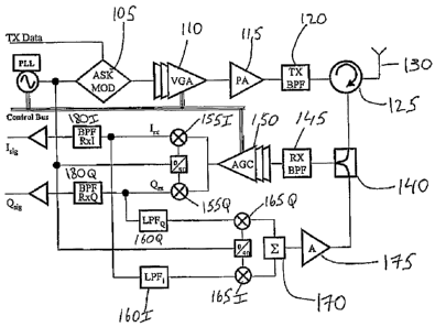
[0015] Figure 2 shows an exemplary embodiment of a
transceiver component of an RFID system according to the present
invention. The exemplary tranceiver component includes a
feedback loop which serves to minimize the effects of reflection
and coupling on the incoming signal, and resulting in a lower
transceiver VSWR.
[00161 The transmitter portion of an RFID transceiver may
create an interrogation signal for transmission by using a
modulator 105 and a variable gain amplifier {"VGA") 110 to
modulate a carrier signal. Use of the VGA 110 may result in an
amplitude modulated (AM) carrier wave. This modulated carrier
wave may then be sent to a power amplifier 115 and band-pass
4
CA 02542983 2006-04-19
WO 2005/041425 PCT/US2004/034739
filter 120. This amplified and filtered modulated carrier wave
may then be sent to a circulator or coupler element 125 for
transmission to the antenna 130.
[001.7] This transmitted interrogation signal may then reflect
off of an RF tag which has been attached to or associated with a
piece of equipment or other commodity. These reflections, which
carry information to identify the tag, may be received by the
antenna 130. In an ideal RFID tranceiver, these received
reflections constitute the whole of the signal received by the
antenna 1.30. However, in deployed RFID systems, the received
signal also contains an error component comprised of
interrogation signal energy which has been coupled from the
transmitter, reflected from the antenna 130, and reflected from
objects in the environment other than the RF tag.
[0018] The incoming signal may arrive at the antenna 130
containing both valuable information from an RF tag and an error
signal. Tn the exemplary embodiment of the present invention,
this composite signal may be sent through a circulator 125 which
may route the incoming signal into one input of an RF combiner
140. The combiner 140 may add this incoming signal to the autput
of the feedback circuit discussed below, and may feed the sum of
these two signals into a band-pass filter 145. The band-pass
filter 145 removes signal. components outside of the frequency
range of the modulated data signal of interest.
laoxs] The signal may then be amplified by an automatic gain
control ("AGC") 150. This amplified signal rnay then be carrier-
demodulated in guadrature using a demodulator 155. Both of the
resulting demodulated signals (the in-phase signal Irx and the
quadrature signal Qrx) may then be split. Two separate branches
CA 02542983 2006-04-19
WO 2005/041425 PCT/US2004/034739
may take the in-phase and guadrature signals through band-pass
filters 1801 and 180Q before continuing towards the transceiver
output for further processing by the base-band decoder 20.
[0020 Each of these branches includes a second path as input
for a feedback loop. The feedback loop achieves echo
cancellation in the transceiver by isolating the noise (error)
component of the incoming signal using low-pass filters 1601 and
160Q, subjecting this signal to a phase inversion, and then
combining it with the incoming signal using another input of the
RF combiner 140. The required phase inversion may be
accomplished by modulating the physical path length of the return
loop. For example, the'path length may be controlled by either
controlling the microwave traces on the circuit board at the
design phase, or by adding a variable delay element for adaptive
control. The feedback loop may be designed to converge with the
incoming signal within the impulse response time of the low-pass
filter, which is usually within a few cycles of the carrier
signal.
[002.] After beginning the feedback loop, both the in-phase
signal Trx and the quadrature signal Qrx may first be passed
through low-pass filters 1602 and 160Q. These low-pass filters
may isolate the undesirable echo signal since the majority of the
base band error signal is of a lower frequency than the signal of
interest. In this example, the error signal is of a lower
frequency and therefore low pass filters are used. However,
there may be other implementations where the error signal is in a
defined range of frequencies and a band-pass filter may be used
or where the error signal is a higher frequency signal and a high
pass filter is used. The outputs of these low-pass filters 160T
and 160Q may then be modulated using modulator 165. The two
6
CA 02542983 2006-04-19
WO 2005/041425 PCT/US2004/034739
signals may then be combined using a summing element 170. The
resulting signal may then be passed through feedback amplifier
175 and the amplified signal may be fed into another input of RF
combiner 140. This closes the feedback loop. The feedback
signal may combine with the incoming signal in a manner which
cancels out the noise component of the incoming signal, leaving
only the modulated data reflected from the RF tag.
[0022 Figure 3 shows an alternative exemplary embodiment of
the present invention. This embodiment may achieve similar
results using a lower number of overall elements by replacing the
circulator element 7.25 and the RF splitter 140 depicted in Figure
2 with a 4-way directional coupler 205. The interrogation signal
is synthesized in this embodiment in the same manner described
for Figure 2 above. The incoming signal from the antenna 130 may
be sent into one port of the coupler 205 which in turn may pass
this incoming signal to output port R of the coupler 205. The
signal path from that point is the same as that described in
Figure 2 above, beginning with the receiver band-pass filter 145.
[00237 The exemplary embodiment of the present invention
shown in Figure 3 may be more cost-effective than that shown in
Figure 2, either by reducing the number of components in the
transceiver or by substituting less expensive yet equally
effective components for more expensive ones. However, this
arrangement may introduce other problems such as non-linearity
and amplification of harmonics. The non-linearity may be
controlled by recording it digitally and then adding a correction
factor into the feedback loop. Amplified harmonics may be
controlled by adding a low-pass filter (not shown) to the output
of the feedback amplifier 175.
7
CA 02542983 2006-04-19
WO 2005/041425 PCT/US2004/034739
[002] Figure 4 shows a second alternative exemplary
embodiment of the present invention with a sample and hold
circuit 305 inserted into the feedback loop. Both the outgoing
and incoming signal paths are the same in this embodiment as
those described in Figures 2 and 3 above; in addition, however,
the sample and hold circuit 305 (shown as sample and hold
components 305I and 305Q) may be inserted in the feedback loop in
between the low-pass filters 160I and 160Q. The sample and hold
circuit 305 may cancel the static reflection components of the
received signal by activating its hold mode when the transceiver
is receiving a backscatter signal. While the sample and hold
circuit 305 may not cancel noise components caused by slow
movements in the environment, the effects of these movements may
be minimized due to the long duration of such reflection changes
relative to the hold periods of the circuit. The sample and hold
circuit 305 may also result in an overall reduction in noise
caused by coupling between the In--phase (Irx) and Quadrature
(Qrx) components of the received signal.
[0025] Figure 5 shows a third alternative exemplary embodiment
of the present invention using a base-band digital radio 410 to
accomplish the filtering portion of the feedback loop digitally.
Here, the demodulated In-phase (Irx) and Quadrature (Qrx)
components of the received signal may be converted into digital
signals using analog-to-digital converters 4~.5I and 415Q. The
output signal path from the transceiver 10 to the base band
processor 20 is the same as in the previous embodiments, except
that the low-pass filters 420I and 420Q are implemented as
digital components in the base band digital radio 410.
a
CA 02542983 2006-04-19
WO 2005/041425 PCT/US2004/034739
[0026] In the feedback portion of the signal path, these
digital signals may then be filtered using digital low-pass
filters 4201 and 420Q contained in the base-band digital radio
47Ø The output of these filters may then be converted back into
analog signals using digital-to-analog converters 4252 and 425Q.
These converters may inherently perform the echo cancellation
performed by the sample-and-hold circuit 305 in Figure 4. Thus,
the inclusion of the base band digital radio 4~.0 in this
exemplary embodiment obviates the need for a sample-arid-hold
circuit of the kind presented in Figure 4.
[00277 Figure 6 shows a fourth exemplary embodiment of the
present invention. This exemplary embodiment creates the
outgoing interrogation signal in a manner identical to the
previous embodiments, except that a power amplifier biasing
element 505 and a power output detector 510 are added to allow
for precise digital control of output power. A temperature
monitor 515 may also be included to prevent overheating. This
embodiment also includes a Tx video 501 input which is an analog
signal generated by a D/A converter. The Tx video 501 input is
the analog equivalent of the Tx Symbol input referred to in Fig.
5. The Tx Mute 503 input allows the transmitter to be turned off
and is independent of the receiver, i.e., the receiver may be
listening to other transmissions while the transmitter is shut-
off. The ALC (automatic level control) 507 performs the same
function as the VGA ~.l0~described with reference to the previous
embodiments.
[0028] In the present exemplary embodiment the incoming
signal may again be passed through a band-pass filter 145 and an
AGC element 150. The signal may then be demodulated in-phase and
in-quadrature using demodulators 1551 and 155Q. The resulting
9
CA 02542983 2006-04-19
WO 2005/041425 PCT/US2004/034739
base band signals may be passed through low-pass filters 160I and
160Q. The low pass filters 1601 and 160Q are anti-aliasing
filters for the D/A converters. This exemplary embodiment may
utilize the digital sub-system (shown in detail in Figure 7) to
perform other functions. For example, digital filtering of the
Irx and Qrx video signals 520I and 520Q in order to drive the
feedback path and to enable real-time adaptation of the system
depending on the multi-path signal propagation conditions.
[00293 The RF echo cancellation low pass filters may be
digitally implemented in the baseband portion of the system. The
mufti-path signal propagation conditions change the nature of the
echo signals from non-RFID elements that may be moving around in
the environment. Thus, a digitally implemented adaptive filter
may be advantageous. The inputs for adaptation may be a
calibration period that sends out a known signal while obtaining
reflections from known tags. For example, a known tag may be
affixed to a known location on the wall near a docking bay
portal. The digital system may also continuously re-calibrate
the feedback loop by monitoring the video signals 520I and 520Q
for imbalances. When such imbalances are detected the digital
system may compute gain, phase, and offset correction factors,.
and then apply these factors to the feedback loop using Icancel
and Qcancel signals 525I and 525Q.
[0030] The embodiment of Fig. 6 also shows a balanced
amplifier 512 in the feedback loop. The balanced amplifier may
operate in the same manner as the amplifier 175 described with
reference to the previous embodiments. However, the balance
amplifier 512 may be used for impedance matching to the low pass
filtex 514. It shauld be understood that the low pass filter 514
is optional and does not need to be included in the feedback loop
CA 02542983 2006-04-19
WO 2005/041425 PCT/US2004/034739
of this embodiment. In the event that the low pass filter 514 is
not included, the balanced amplifier 5.12 may still be used to
match impedance to the coupler 205 to reduce non-linearities.
j00311 Figure 7 shows the sub-system interfaces through which
the transceiver described by the present invention may interact
with other components of an RFID system 1. A data conversion
block 600 may provide a simple analog signal interface with
digital controls. A programmable logic device 605 may provide a
parallel interface to a digital signal processor 610. An MCU 615
may provide additional user controls and interfaces with the
transceiver and other components. The MCU 61.5 may provide the
protocol for the communications between the reader and the tag
including mufti-tag arbitration. Such protocols may include
those published by the UCC (Uniform Code Council), EAN (European
Article Numbering?, and. ISO (International Standards
Organization). The MCU 615 may also provide packet data
synthesis for conversion to a bit stream that may be bit encoded,
modulated and transmitted by the transceiver, provide frequency
hopping and channel access protocols, provide automatic gain
control for a maximum signal to noise ratio and dynamic range of
the received signal and provide automatic level control for
transmission power control far power savings, interference
mitigation, user selectable power profiling, and any applications
where power control is advantageous.
[0032] It will be apparent to those skilled in the art that
various modifications and variations can be made in the structure
and the methodology of the present invention, without departing
from the spirit or scope of the invention. Thus, it is intended
that the present invention cover the modifications and variations
of this invention provided they come within the scope of the
11
CA 02542983 2006-04-19
WO 2005/041425 PCT/US2004/034739
appended claims and their equiva7.ents.
7.2