Note: Descriptions are shown in the official language in which they were submitted.
CA 02543023 2006-04-12
05AB181
DC VOLTAGE BALANCE CONTROL FOR THREE-LEVEL NPC POWER
CONVERTERS WITH EVEN-ORDER HARMONIC ELIMINATION SCHEME
REFERENCE TO RELATED APPLICATION
This application claims priority to and the benefit of U.S. Provisional Patent
Application Serial No. 60/671,714, filed April 15, 2005, entitled DC VOLTAGE
BALANCE CONTROL FOR THREE-LEVEL NPC INVERTER WITH SELECTIVE
HARMONIC ELIMINATION SCHEME, the entirety of which is hereby incorporated by
reference.
FIELD OF THE INVENTION
The present invention relates generally to electrical power conversion, and
more
particularly to controls and methods for pulse width modulated operation of
three-level
inverter and rectifier type power converters.
BACKGROUND OF THE INVENTION
Power converters have been extensively employed in medium voltage motor
drives and other applications in which electrical power needs to be converted
from DC
to AC or vice versa. Such conversion apparatus is commonly referred to as an
inverter
for converting DC to AC, or alternatively as a rectifier if the conversion is
from AC to
DC power, where the AC power connection typically provides a multi-phase
output or
input, respectively. Multi-phase converters are often constructed using an
array of
high-voltage, high-speed switches, such as gate-turnoff thyristors (GTOs),
insulated-
gate bipolar transistors (IGBTs) or other semiconductor-based switching
devices,
which are selectively actuated through pulse width modulation (PWM) to couple
the AC
connections with one or the other of the DC bus terminals, where the timing of
the
array switching determines the power conversion performance. In medium voltage
motor drive applications, the timed control of the switch activations in
advanced
inverter type power converters is used to provide variable frequency, variable
-1-
CA 02543023 2006-04-12
05AB181
amplitude multi-phase AC output power from an input DC bus, whereby driven
motors
can be controlled across wide voltage and speed ranges.
Neutral point clamped (NPC) converters include two similarly sized high
voltage
capacitors connected in series between the DC bus lines, with the capacitors
being
connected to one another at a converter "neutral" point node. In these NPC
converters, three-level switching control is often used to provide three
switching states
for each AC terminal, with the AC terminal being selectively coupled to either
of the DC
terminals or to the neutral node. Three-level switching techniques allow
higher
operating voltages along with better (e.g., lower) total harmonic distortion
(THD) and
electromagnetic interference (EMI) than do comparable two-level inverter
designs.
Several PWM switching techniques have been used in high or medium voltage NPC
power converters to control the switch array, wherein space vector modulation
(SVM)
approaches are increasingly used because of good harmonic profile, effective
neutral
point potential control, and ease of digital implementation. In NPC power
converters, it
is desirable to maintain the neutral voltage at a constant level with the two
capacitor
voltages being substantially equal, a goal known as neutral point balancing.
Problems
may arise if the voltage at the NPC inverter neutral point deviates from the
mid-point of
the DC bus, including stresses to components of the converter itself and/or to
devices
being powered by the converter, as well as adding harmonic distortion to the
output of
the inverter. To control the neutral point voltage, many converters are
equipped with
feedback control apparatus. However, such closed loop neutral balancing
approaches
are costly, requiring feedback sensing apparatus and advanced control
algorithms to
regulate the neutral voltage while also providing the desired AC
outputwaveforms. In
addition to neutral point balancing, it is desirable to minimize the operating
frequencies
of the array switches. These problems are of course balanced against
frequency,
amplitude, and other performance and control requirements for a given
converter
application. Thus, there remains a continuing need for improved three-level
power
converters as well as SVM methods and control systems for operating power
-2-
CA 02543023 2006-04-12
05AB181
converters for use in medium voltage motor drives and other applications
requiring
electrical power conversion.
SUMMARY OF INVENTION
One or more aspects of the invention are now summarized to facilitate a basic
understanding of the invention, wherein this summary is not an extensive
overview of
the invention, and is intended neither to identify certain elements of the
invention, nor
to delineate the scope thereof. The primary purpose of the summary, rather, is
to
present some concepts of the invention in a simplified form prior to the more
detailed
description that is presented hereinafter. The present invention is related to
PWM
control of three-level power converters, in which space vector modulation
(SVM) is
used to control the converter switches. Three-level NPC converters and control
systems are provided, along with methods for providing three-level switching
control
signals to balance the neutral point voltage by space vector modulation in
open-loop
fashion without the added cost, size, and weight of feedback neutral balancing
control
components. The invention may be advantageously implemented in rectifier
and/or
inverter applications in order to facilitate cost effective high or medium
voltage power
conversion with neutral point voltage balancing, low THD and EMI, and the
other
performance advantages of three-level SVM converters.
In accordance with one or more aspects of the invention, a three-level SVM
NPC power conversion system is provided, which can be an inverter for DC-to-AC
conversion or a rectifier for converting AC power to DC. The system includes a
DC
connection, a multi-phase AC connection, and a three-level switching network
coupled
therewith, along with a control system providing SVM switching control signals
to
balance the neutral voltage in open-loop fashion. The DC connection has first
and
second terminals for receiving or supplying DC power, as well as first and
second
capacitors coupled in series between the DC terminals, where the capacitors
are
coupled at a common node or neutral point. The AC connection supplies or
receives
multi-phase electrical power via three or more AC terminals, where the
switching
-3-
CA 02543023 2006-04-12
05AB181
network comprises sets of switching devices associated with the AC phase
terminals.
The switches are actuated by switching control signals from the control system
to
selectively couple the AC terminals to one of the DC terminals or to the
neutral
common node, where the control system provides the sets of switching control
signals
by space vector modulation so as to equalize the voltages across the
capacitors in
open-loop fashion during operation of the power conversion system. .In one
implementation, the control system has a space vector modulation system to
provide
the switching control signals according to an even-order harmonic elimination
(EHE)
vector switching sequence providing half-wave symmetry to balance the voltage
at the
common node, with the vector switching sequence defining a sequence of
switching
states for each segment of an SVM diagram where vector switching sequences for
diametrically opposite diagram segments provide symmetrically opposite
coupling of
the AC terminals with the DC terminals.
Further aspects of the invention relate to a space vector modulation control
system for providing switching control signals to a three-level power
conversion
system. The control system includes drivers for selective actuation of the
converter
switches, as well as switch control means that controls the drivers by space
vector
modulation to balance the voltages across the converter capacitors in open-
loop
operation. In one embodiment, the switch control means comprises an even-order
harmonic elimination vector switching sequence, and processing means for
controlling
the drivers according to a voltage reference vector and according to the
vector
switching sequence.
Still other aspects of the invention provide a vector switching sequence for
space vector modulation of the switching network in a three-level power
conversion
system. The vector switching sequence is comprised of a machine readable
medium
including vector sequence listings for each segment of a space vector
modulation
diagram defining stationary space vectors representing switching states for
the
switching network and defining a plurality of sectors positioned around an
origin of the
space vector modulation diagram. The individual sectors have a plurality of
triangular
-4-
CA 02543023 2006-04-12
05AB181
segments (e.g., 6 in one example), with each segment being defined by a unique
set of
three space vectors at the corners of the triangle, where the individual
vector sequence
listings define a sequence of switching states corresponding to the three
space vectors
defining each segment, with the vector switching sequences defined for diagram
segments that are symmetrically opposite with respect to the diagram origin
including
symmetrically opposite switching states.
Further aspects of the invention relate to a method for space vector
modulation
control of a three-level power conversion system. The method comprises
providing a
space vector modulation vector switching sequence that includes vector
sequence
listings for each segment of the space vector modulation diagram, with the
individual
vector sequence listings defining a sequence of switching states corresponding
to the
three space vectors defining each segment, where the vector switching
sequences
defined for diagram segments that are symmetrically opposite with respect to
the
diagram origin comprise symmetrically opposite switching states. The method
further
includes obtaining a reference vector, which represents a desired state of the
power
conversion system, and determining the reference vector segment location in a
space
vector modulation diagram. Switching control signals are provided to the power
conversion system according to the vector sequence listing for the reference
vector
segment location.
BRIEF DESCRIPTION OF THE DRAWINGS
The following description and drawings set forth certain illustrative
implementations of the invention in detail, which are indicative of several
exemplary
ways in which the principles of the invention may be carried out. The
illustrated
examples, however, are not exhaustive of the many possible embodiments of the
invention. Other objects, advantages and novel features of the invention will
become
apparent from the following detailed description of the invention when
considered in
conjunction with the drawings, in which:
-5-
CA 02543023 2006-04-12
05AB181
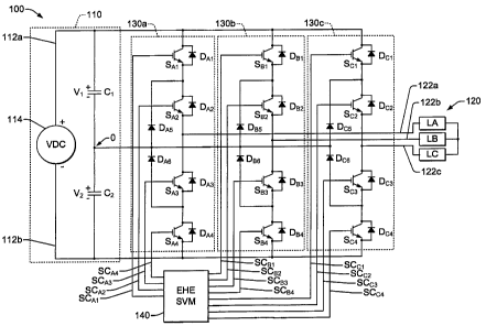
Fig. 1A is a schematic diagram illustrating an exemplary three-level inverter
type
DC to AC power conversion system having space vector modulation (SVM) switch
control apparatus providing open-loop suppression of even-order harmonics and
neutral point voltage balancing in accordance with one or more aspects of the
present
invention;
Fig. 1 B is a schematic diagram illustrating an exemplary three-level SVM
rectifier for converting multi-phase AC to DC electrical power using an even-
order
harmonic elimination (EHE) SVM switch control system in accordance with the
invention;
Fig. 1 C is a schematic diagram illustrating an exemplary SVM control system
of
the power converters of Figs. 1A and 1B, including drivers for actuating the
power
converter switches and a processor that controls the drivers by space vector
modulation according to an EHE SVM vector switching~sequence in order to
balance
the voltages across the capacitors and reduce even-order harmonics in open-
loop
operation of the power conversion system according to various aspects of the
invention;
Fig. 1 D is a table showing dwell time computations for the SVM control system
of Figs. 1A-1C;
Fig. 1 E is a table showing an exemplary switching sequence along with the
corresponding dwell times for a specific SVM diagram segment;
Fig. 1 F is a flow diagram illustrating an exemplary method for SVM control of
a
three-level power conversion system according to further aspects of the
invention;
Figs. 2A and 2B are schematic diagrams illustrating an exemplary EHE SVM
vector switching sequence for providing open-loop even-order harmonic
suppression
and neutral balancing using half-wave symmetric sequence entries according to
other
aspects of the invention;
Figs. 3 and 4 are schematic diagrams illustrating an exemplary SVM diagram
showing space vectors that represent switching states for the power converter
switching network and define six sectors with six triangular segments per
sector;
-6-
CA 02543023 2006-04-12
05AB181
Fig. 5 is a graph illustrating exemplary simulated half-wave symmetric phase
voltage waveforms VAO and VAB for the three phase inverter of Fig. 1A as the
reference
vector rotates in one full cycle;
Fig. 6 is a graph illustrating simulated even-order harmonic content of an
inverter line-to-line waveform in a three-level SVM controlled inverter using
a
conventional SVM switching control scheme;
Fig. 7 is a graph showing simulated even-order harmonic content in a three-
level SVM controlled inverter such as the one in Fig. 1A using the SVM control
system
of Fig. 1 C and the EHE SVM vector switching sequence of Figs. 2A and 2B;
Fig. 8 is a graph illustrating simulated comparative total harmonic distortion
(THD) performance for a conventional SVM approach and for an SVM modulation
control system of Fig. 1C using the EHE SVM vector switching sequence of Figs.
2A
and 2B;
Fig. 9A is a graph illustrating experimental line-to-neutral and line-to-line
voltage
waveform plots in a three-level SVM controlled inverter using a conventional
SVM
switching control scheme;
Fig. 9B is a graph corresponding to Fig. 9A showing experimental odd and
even-order harmonic content plots in the SVM inverter using the conventional
SVM
switching control scheme;
Fig. 10A is a graph illustrating experimental line-to-neutral and line-to-line
voltage waveform plots in a three-level SVM controlled inverter such as the
one in Fig.
1A using the SVM control system of Fig. 1C and the EHE SVM vector switching
sequence of Figs. 2A and 2B;
Fig. 10B is a graph corresponding to Fig. 10A illustrating experimental odd
and
even-order harmonic content plots in the SVM inverter, with significant even-
order
harmonic suppression; and
Fig. 11 is a graph showing plots of experimental comparative voltage balancing
situations for the conventional and EHE SVM techniques.
-7-
CA 02543023 2006-04-12
05AB181
DETAILED DESCRIPTION OF THE INVENTION
Referring now to the figures, several embodiments or implementations of the
present invention are hereinafter described in conjunction with the drawings,
wherein
like reference numerals are used to refer to like elements throughout, Fig. 1A
illustrates an exemplary three-level inverter power conversion system 100,
including a
DC connection 110, a three-phase AC connection 120, and a three-level
switching
network 130 including switch sets 130a, 130b, and 130c collectively coupling
the DC
and AC connections 110 and 120, respectively. The conversion system 100
further
includes space vector modulation (SVM) switch control apparatus 140 that
provides
open-loop suppression of even-order harmonics to effectively balance a neutral
point 0
(zero) of the DC connection 110 in accordance with one or more aspects of the
invention. The DC connection 110 comprises first and second DC terminals 112a
and
112b, respectively, for receiving DC power from a source 114, as well as first
and
second capacitors C1 and C2 coupled in series between the terminals 112, where
the
capacitors C1 and C2 are coupled at the common node or neutral point 0. The
voltage
across the terminals 112 can be referred to as a DC bus voltage, where the
capacitors
C1 and C2 are preferably of the same or substantially equal capacitance and
voltage
ratings, whereby the neutral point 0 ideally is at a voltage half-way between
the
voltages at the bus terminals 112 (e.g., at the mid-point of the DC bus
voltage). The
source 114 can be any source of DC power, with or without ripple voltages or
otherAC
components, such as the output of a rectifier bridge, a switching rectifier
that receives
input AC (single or multi-phase) and provides rectified DC to the terminals
112,
batteries, or other DC source. In one application as a medium voltage motor
drive
inverter, the DC bus voltage at terminals 112 can be several thousand volts.
The AC connection 120 includes three AC terminals 122a, 122b, and 122c
coupled to a Y-connected three-phase load including phase loads LA, LB, and
LC,
respectively, such as motor windings in one example. Other multi-phase
implementations are possible, wherein more than three AC terminals 122 are
provided,
with addition of a corresponding number of switch sets, such that each AC
terminal
_g_
CA 02543023 2006-04-12
05AB181
122 is selectively coupleable to one of the DC terminals 112 or to the neutral
point 0
via space vector modulation switch control signals SC from the controller 140.
The
switching network 130 comprises sets 130a, 130b, and 130c of switching devices
SA~-
SA4, Sg~-Sg4, and Sc~-S~4 associated with the AC phase terminals 122a, 122b,
and
122c, respectively, wherein the switching devices S may be any form of
switches that
provide for selective electrical connection in a first state and electrical
isolation in a
second state, for example, GTOs, IGBTs, IGCTs, etc. (IGBTs in the illustrated
embodiments). In the embodiments illustrated herein, moreover, the individual
switching devices S include freewheeling diodes, illustrated in the figures as
Dpi-DA4,
DBE-DB4, and Dc~-Dc4, associated with the switching devices SAC-SA4, Say-Sea,
and Sc~-
Sc4, respectively.
In the illustrated inverter system 100, three sets 130a, 130b, and 130c are
provided, each including four switches S connected in series between the DC
bus
terminals 112a and 112b, so as to provide selective connection of a
corresponding AC
terminal 122 to one of the DC terminals 112 or to the neutral 0. In operation,
the
switches S of each group 130a, 130b, and 130c are activated in pairs to
achieve this
three-level switching functionality for pulse width modulation by SVM
techniques as
described herein. With respect to phase A, for example, switches SAC and SA2
are
connected in series between the first DC terminal 112a and the AC terminal
122a, with
the node between the switches SAi and SA2 being connected to the DC connection
neutral 0 via diode DA5. In addition, switches SA3 and SA4 are Connected in
series
between the AC terminal 122a and the second DC terminal 112b, with the node
between the switches SA3 and SA4 also coupled to the neutral point 0 via diode
DA6. In
this configuration, switching signals SCAB-SCA4 are provided to the control
gates of the
IGBTs Sq~-SA4, respectively, for selective actuation by the control system
140. The
first switch group 130a is provided with certain combinations of the control
signals
SC,q~-SCA4 to achieve one of three switching states, so as to selectively
connect the
first AC phase terminal 122a with either the first (e.g., +) DC terminal 112a,
the neutral
0, or the second (e.g., -) DC terminal 112b, corresponding respectively to a
first
_g_
CA 02543023 2006-04-12
05AB181
switching state with switches SAC and SA2 on, a second switching state with
switches
SA2 and SA3 on, and a third state with switches SA3 and SA4 on. The second and
third
switch sets 130b and 130c are similarly configured and selectively operated
via
corresponding switching signal sets SCB~-SCB4 and SCc~-SCc4, respectively, to
selectively couple the corresponding AC terminal to the first DC terminal
112a, the
neutral 0, or the second DC terminal 112b.
Fig. 1 B illustrates another preferred embodiment of a power conversion system
150 having an input AC connection 160 with terminals 162a, 162b, and 162c, as
well
as a DC output connection 170, in this case an NPC DC connection having DC
terminals 172a and 172b, and two series connected capacitors. C1 ands C2
defining a
center neutral common node 0. The system 150 is constructed as a three-level
NPC
rectifier for converting a multi-phase AC input to DC electrical power using
an even-
order harmonic elimination (EHE) SVM switch control system 140 driving a
switching
network 130 as described above. In this embodiment, a three-phase AC power
source
164 provides phase voltages at AC terminal lines LA, LB, and LC, which is then
converted to a DC bus voltage on DC terminals 172, wherein the switching
network
130 is actuated using the EHE SVM techniques described herein for open loop
balancing of the neutral point voltage.
Referring also to Fig. 1 C, the control system 140 used in the inverter and
rectifier systems 100 and 150 is an even-order harmonic elimination (EHE)
controller
providing the sets of switching control signals SC by space vector modulation.
Any
suitable SVM system 140 can be used that provides neutral point balancing to
equalize
the voltages across the capacitors C1 and C2 in open-loop fashion during
operation of
the power conversion system 110, 150. The embodiment 140 is a processor-based
system that includes memory (not shown) for storing data and instructions to
carry out
the functionality described herein, although other processing apparatus can be
used,
such as programmable logic, etc. As shown in Fig. 1 C, the exemplary
controller 140
provides a space vector modulation system with a processor 142 that controls
isolated
driver circuits or other driver means.144 for selectively actuating the
switches S in the
-10-
CA 02543023 2006-04-12
05AB181
power converter switching network 130 for selective coupling of individual AC
terminals
122, 162 to one of the DC terminals 112, 172 or the common node 0. The
processor
142 can be any type of processing device, logic circuit, software, firmware,
or
combinations thereof, which forms a switch control means along with an SVM EHE
vector switching sequence 146 for controlling the drivers 144 to balance the
voltages
across the capacitors C1 and C2 in open-loop fashion, in this case, by
providing half-
wave symmetric switching of the network 130, for both the case of an inverter
100 (Fig.
1A) or a rectifier (Fig. 1 B). The switching sequence 146 can be a file, a
data structure,
a set of machine readable instructions or values, or any other representation,
whether
hardware, software, or combinations thereof that represents vector sequence
listings
for each segment of a space vector modulation diagram.
Referring also to Figs. 3 and 4, an exemplary space vector modulation diagram
200 is shown. In operation of the power converter 100, 150, the processor 142
of Fig.
1 C controls the drivers 144 according to a reference vector VREF (Fig. 4) and
according
to the EHE SVM vector switching sequence 146. In particular, the drivers 144
and
hence the switching network 130 are controlled according to the current
position of
VREF in the space vector modulation diagram 200, which has 19 stationary space
vectors VO-V18 that represent 27 switching states for the three-level
switching network
130. The zero vector (VO) at the diagram center or origin has a magnitude of
zero and
includes three redundant switching states [PPP], [000], and [NNN], with the
first
numeral representing the switching state of the first switch set 130a (Fig.
1A), the
second numeral corresponding to the second switch set 130b, and the third
numeral
representing the switching state of switch set 130c. In this regard, the
numerals "0"
represent the case where the corresponding switch set 130 connects the AC
terminal
122 to the neutral 0 (e.g., switches SA2 and SA3 on in switch set 130a).
Numerals "P"
(e.g., positive) represent the case where the corresponding switch set 130
connects
the AC terminal 122 to the first (+) DC terminal 112a (switches SAC and SA2
on), and
the numerals "N" (e.g., negative) represent the case where the corresponding
switch
set 130 connects the AC terminal 122 to the second (-) DC terminal 112b
through
-11-
CA 02543023 2006-04-12
05AB181
corresponding actuation of a suitable pair of the switches S (switches SA3 and
SA4 on).
The diagram 200 of Figs. 3 and 4 includes small vectors V1 to V6, all having a
magnitude of Vd/3, and comprising two redundant switching states, one
containing [P]
and the other containing [N], and can therefore be alternatively indicated in
the
switching sequence (in Figs. 2A and 2B below) as a P or N-type small vector,
where
Vd is the DC bus voltage at the terminals 112. In addition, the diagram 200
provides
medium vectors V7 to V12, each having a magnitude of 3-2Vd/3, as well as large
vectors V13 to V18), all having a magnitude of 2Vd/3.
The diagram 200 of Figs. 3 and 4 is a two-level hexagon that defines six
sectors
(SECTOR 1 through SECTOR 6 in Fig. 4) positioned around the origin (the
diagram
center corresponding to the zero vector VO), with the sectors each having six
triangular
segments labeled K-1 a, K-1 b, K-2a, K-2b, K-3, and K-4, where K is the sector
number
(1 through 6), as best shown in Fig. 4. Each segment is defined by a unique
set of
three space vectors V at the corners of the corresponding triangle, where the
triangular
segments 1-1a and 1-1b are formed as a subset, each corresponding to the
triangle
formed by vectors V0, V1, and V2, and other such subsegments are accordingly
defined in the diagram 200. The position of the reference vector VREF at any
given
time is ascertained by the SVM controller processor 142, which then consults
the
corresponding entry list in the switching sequence 146 for selectively
sequencing the
switching control signals SC through various combinations of three-level
patterns
corresponding to the three defining space vectors V for the current segment to
implement the space vector modulation of the switching network 130. Further,
the
durations of the switching patterns (dwell times) are determined according to
the
particular VREF position within the given triangular diagram segment, taking
into
account the proximity of the reference vector VREF to each of the three
defining space
vectors V.
Referring also to Figs. 1 D and 1 E, the exemplary reference vector location
in
segment 1-2a of Fig. 4 provides a vector modulation involving the defining
vectors V1,
V2, and V7. The times Ta, Tb, and Tc during which the controller 140 dwells at
a
-12-
CA 02543023 2006-04-12
05AB181
particular switching state for V1, V7, and V2, respectively, are computed
according to
the relationship V1 Ta + V7Tb + V2Tc = VrefTs, where the sample period Ts = Ta
+ Tb
+ Tc and Ts is computed according to the selected rotational frequency of the
reference vector VREF (Ts = 1/f according to the sampling frequency f of the
inverter
system 100). Knowing the sample period Ts and the modulation index ma, the
dwell
times for a given segment are computed according to the formulas in table 148a
of Fig.
1 D, and the switching state sequence and corresponding times are shown in
table
148b of Fig. 1 E for the exemplary reference position with VREF in diagram
segment 1-
2a. In this manner, the SVM control system 140 performs space vector
modulation of
the network switches 130 according to the reference vector position and
according to
the EHE vector switching sequence 146.
Figs. 2A and 2B illustrate further details of the exemplary EHE SVM vector
switching sequence 146, which provides open-loop even-order harmonic
suppression
or elimination (EHE) through half-wave symmetric sequence entries. In this
regard, the
inventors have appreciated that half-wave symmetry in the SVM switching
sequence
146 facilitates reduction of even order harmonics in the AC power, and further
that
even-order harmonic elimination enhances the neutral voltage balance in the DC
connection 110, 170 without requiring feedback control for NPC converters 100,
150.
Moreover, the exemplary sequence 146 of Figs. 2A and 2B provides this open-
loop
even-order harmonic elimination through careful selection of the sequence
entries for
the SVM diagram segments. The vector switching sequence 146 can be any form of
data store, list, database, file, etc., according to which a three-level NPC
power
conversion system can be operated with open-loop neutral voltage balancing.
In the illustrated embodiments, the sequence 146 is comprised of a machine
readable medium, such as processor readable memory for example, that includes
vector sequence listings for each of the six segments defined by the SVM
diagram
200, where the individual listings are shown as seven-entry columns in the
table format
representation in Figs. 2A and 2B. While the individual vector sequence
listings for
each segment include seven switching state entries in the exemplary sequence
146,
-13-
CA 02543023 2006-04-12
05AB181
other embodiments are possible, in which any number of three or more entries
can be
provided for each sector-specific listing. The row and column format
illustrated in Figs.
2A and 2B is merely for ease of understanding, and the actual sequence 146 may
be
stored in any suitable format by which a sequence can be indexed according to
the
reference vector sector location. Moreover, while the listings each define a
sequence
of switching states corresponding to the three space vectors defining the
corresponding diagram segment with switching states provided for each of three
AC
connection phase terminals 122, 162, other embodiments may be constructed for
converters having more than three AC phases, wherein the corresponding entries
in
the sequence 146 will be provided with a corresponding number of additional
numeral
entries (P, 0, or N).
To illustrate operation of the sequence 146 when employed in the above
converter embodiments, it is initially noted that the entry for sector 1-2a in
Fig. 2A
provides a succession of vectors V~p, V~, V2N, VAN, V2N, V7, and VIP defining
three-level
SVM switch states P00, PON, OON, ONN, OON, PON, and P00, respectively. In the
illustrated sequence 146, moreover, the vector switching sequences defined for
diagram segments that are symmetrically opposite with respect to the diagram
origin
(diametrically opposite segments) comprise symmetrically opposite switching
states.
Thus, as seen in Fig. 4, the sector 4-2a is diametrically opposite the
reference vector
segment 1-2a. As seen in the sequence 146 in Fig. 2B, the entry for sector 4-
2a in
Fig. 2A provides symmetrically opposite switching states N00, NOP, OOP, OPP,
OOP,
NOP, and N00 through successive provision of vectors V4N, V~o, V5P, V4P, VsP,
V~o, and
V4N, respectively. In this manner, half-wave symmetry is ensured at the AC
connections 120, 160, resulting in suppression or substantial elimination of
even-order
harmonics and neutral point voltage balance at the DC connections 110, 170.
This
balancing, moreover, is achieved in open-loop fashion, whereby complicated and
costly closed-loop neutral balance controls are not needed. As seen in Figs.
2A and
2B, the vector sequence listings for each segment include seven switching
state
entries individually indicating one of three possible switching state levels
positive (P),
-14-
CA 02543023 2006-04-12
05AB181
zero (0), or negative (N) for each of the three switching groups 130 (e.g.,
for each AC
phase) in the conversion system, where the vector sequence listings for each
pair of
first and second diagram segments that are diametrically opposite relative to
the
diagram origin (VO) comprise symmetrically opposite switching states, with
positive (P)
levels in the entries of the listing for the first segment corresponding to
negative (N)
levels in the entries of the listing for the second segment and vice versa. In
this
manner, as the reference vector rotates around one revolution of the space
vector
diagram 200, the individual phase voltage waveforms (both line-to-line and
line-to-
neutral) include a positive half cycle and a symmetrical negative half-cycle,
as
illustrated and described further below with respect to Figs. 5, and 10A.
Turning now to Fig. 1 F, an exemplary method 180 is illustrated for space
vector
modulation control of a three-level power conversion system according to
further
aspects of the invention. While the method 180 is illustrated and described
below in
the form of a series of acts or events, it will be appreciated that the
various methods of
the invention are not limited by the illustrated ordering of such acts or
events. In this
regard, except as specifically provided hereinafter, some acts or events may
occur in
different order and/or concurrently with other acts or events apart from those
illustrated
and described herein in accordance with the invention. It is further (noted
that not all
illustrated steps may be required to implement a process or method in
accordance with
the present invention, and one or more such acts may be combined. The
illustrated
methods and other methods of the invention may be implemented in hardware,
software, or combinations thereof, in order to provide the SVM modulation
control
functionality described herein, and may be employed in any three-level pulse
width
modulated NPC power conversion system including but not limited to the above
illustrated systems 100 and 150, wherein the invention is not limited to the
specific
applications and embodiments illustrated and described herein.
The method 180 is performed in a generally continuous loop fashion, where a
current sample control period begins at 182 by obtaining the reference vector
VREF
representing the desired state of the power conversion system. The method 180
-15-
CA 02543023 2006-04-12
05AB181
continues at 184 where the reference vector segment location (sector and
segment) in
the SVM diagram 200 is determined. Based on the current location of VREF,
switching
control signals are provided at 186 to the power conversion system according
to a
vector sequence listing forthe reference vector segment and sector location,
where the
sequence listing provides for half-wave symmetrical sequence definitions. In
the
illustrated example, the provision of the switching control signals at 186
comprises
obtaining a vector switching sequence listing at 188 that corresponds to the
reference
vector location from an SVM vector switching sequence that includes sequence
listings
defined for diametrically opposite diagram segments that comprise
symmetrically
opposite switching states, as in the exemplary sequence 146 in Figs. 2A and 2B
above. At 190, switching times are computed (e.g., Ta, Tb, and Tc above) for
application of the individual switching states of the vector sequence list in
the current
sample control period, and the switching states of the vector sequence list
are applied
at 192 to control the power conversion system according to the computed
switching
times. Thereafter, the next control period starts at 194 and the process 180
repeats
for subsequent control cycles as described above.
Referring now to Figs. 5-8, simulated results are illustrated for the three-
level
NPC SVM inverter of Fig. 1A using the above described EHE modulation concepts
of
the invention. The NPC inverter 100 was simulated for a power rating of 1 MVA
and
operation at.an AC output frequency of 60 Hz, with three-phase loads LA, LB,
and LC
individually including series connected 17.3 OHM resistors and 2.3 mH
inductors. The
simulated input DC voltage at terminals 112 was 5600 volts DC, using 2400 NF
capacitors C1 and C2 with a sampling frequency of 1.44 KHz. Fig. 5 illustrates
a graph
300 showing the resulting simulated line-to-line and line-to-neutral phase
voltage
waveforms VAO and VAg for a full cycle in the inverter 100, showing the half-
wave
symmetry that may be achieved by the careful definition of the switching
sequence
146. As noted above, the inventors have found that this half-wave symmetry
reduces
the even order harmonics, and also results in effective neutral-point voltage
balancing
without need for closed loop adaptation.
-16-
CA 02543023 2006-04-12
05AB181
To illustrate this performance advantage, Fig. 6 provides a graph 400
illustrating
even-order harmonic content of the line-to-line waveform, plotted as a
function of
modulation index MI, in a similarly designed three-level SVM modulated
inverter using
a conventional SVM switching control scheme. In this graph 400, Vpg,~ is the
rms
value of the nth order harmonic, Vqg,1,M,qx IS the maximum rms value of the
fundamental component in the line-to-line phase voltage VAB, and MI is the
modulation
index. As can be seen in the graph 400, the even-order harmonics are
significant
using the conventional SVM converter control technique. In this regard, prior
SVM
approaches provided for vector sequence selection with two design
considerations or
goals, primarily to limit the switching frequency of the switches S in the
converter
switching network 130. The first conventional SVM sequence design criteria is
that the
transition from one switching state to the next (within a given segment)
should involve
only two switch changes, one being turned off and the other being turned on.
The
other typical design goal is that transitions from one SVM diagram segment to
the next
should involve a minimum number of switch state changes, preferably two or
less.
These design goals or considerations were taken into account in selecting the
conventional switching sequence used in the simulated performance represented
in
Fig. 6. As noted in the graph 400, however, the conventional SVM approach
produces
a significant amount of even order harmonics, leading to large neutral point
imbalance
problems in three-level power conversion applications.
Referring now to Fig. 7, a graph 500 illustrates the simulated even-order
harmonic content in a three-level SVM controlled inverter such as the inverter
100 of
Fig. 1A using the SVM control system 140 of Fig. 1C with the EHE SVM vector
switching sequence 146 of Figs. 2A and 2B. The graph 500 clearly shows that
the
line-to-line voltage VAB produced by using the half-wave symmetrical sequence
146
effectively suppresses or eliminates all the even-order harmonics in the AC
output. As
discussed above with respect to Figs. 2A and 2B, the EHE vector switching
sequence
146 is arranged such that the inverter phase voltage generated by VREF in any
two
regions symmetrical to the origin of the space vector diagram 200 have mirror
image
-17-
CA 02543023 2006-04-12
05AB181
voltages, by which the sequence 146 achieves half-wave symmetry, as shown in
Fig.
5. The simulated results in the graph 500 of Fig. 7 and the waveforms of Fig.
5
illustrate that the EHE SVM system 140 provides open-loop waveform symmetry
along
with even-order harmonic elimination.
Referring also to Fig. 8, the inventors have also simulated the total harmonic
distortion (THD) performance of the sequence 146, as shown in graph 550
illustrating
the VAB THD profiles 552 and 554 produced by the conventional SVM sequence and
the new EHE SVM sequence scheme 146, respectively. As can be seen in the graph
550, the sequence 146 sacrifices essentially little or no THD performance
compared
with the conventional technique, wherein the curves 552 and 554 are nearly
identical.
While not wishing to be tied to any particular theory, it is believed that the
comparable
THD performance is due to the use of the same stationary vector selection and
dwell
time calculations in the two simulated cases. Moreover, the exemplary EHE SVM
sequence 14C of Figs. 2A and 2B satisfies the criteria that the transition
from one
switching state to the next (within a given segment) should involve only two
switch
changes, while relaxing the above-mentioned convention restriction that
transitions
from one SVM diagram segment to the next should involve minimum number of
switch
state changes. However, the device switching frequency of the new sequence 146
is
only slightly higher than that of the conventional scheme for a given sampling
frequency. For example, in the above mentioned simulation conditions, the
device
switching frequency is 750 Hz using a conventional switching sequence, whereas
the
device switching frequency using the illustrated EHE sequence 146 rises to
only 780
Hz, wherein some of the transitions for VREF moving from segment to segment
involve
four switches for the new scheme instead of two for the conventional scheme.
Thus,
while relaxing the second conventional design consideration might at fist seem
undesirable, the provision of the half-wave symmetry by the exemplary EHE
sequence
146 provides significant advantages with respect to neutral point balancing
and even-
order harmonic elimination, while allowing only minor switching frequency
increase,
and without sacrificing THD performance.
-18-
CA 02543023 2006-04-12
05AB181
Referring now to Figs. 9A-11, experimental results also bear out the
performance advantages of the open-loop SVM EHE concepts described above. A
three-level inverter of the type shown in Fig. 1A was evaluated using two
seven-entry
SVM switching sequences for comparison and verification of new EHE SVM
technique.
The first SVM sequence was a conventional SVM scheme having both even-order
and
odd-order harmonics, whereas the second experiment used the EHE, switching
sequence 146, which does not produce even-order harmonics. The experimental
parameters used in both cases include a DC voltage at terminals 112 of 300 VDC
to
produce a line-to-line AC output voltage of 208 VAC, with DC capacitors C1 =
C2 =
4700 uF, and AC phase loading comprising a 3.2 OHM resistor and a 15 mH
inductor,
with a PWM sampling frequency of 1080 Hz, wherein the modulation index MI is
the
peak value of VabIVdc, approximately 0.9 in both experiments. Fig. 9A provides
a
graph 600 illustrating experimental line-to-neutral and line-to-line voltage
waveform
plots Va0 and Vab, respectively, in a three-level SVM controlled inverter
using a
conventional SVM switching control scheme, and Fig. 9B shows a corresponding
graph 610 illustrating experimental line-to-neutral and line-to-line voltage
odd and
even-order harmonic content plots in the SVM inverter using the conventional
SVM
switching control scheme. As shown in the waveform plots of graph 600, the
conventional SVM technique fails to provide waveform symmetry, and the plot
610 of
Fig. 9B illustrates the presence of significant even-order harmonics in the AC
output.
Figs. 10A and 10B shown comparative plots 700 and 710, respectively, using
the above described EHE SVM approach for open loop even-order harmonic
suppression (e.g., employing the sequence 146 of Figs. 2A and 2B). The graph
700 in
Fig. 1 OA illustrates experimental line-to-neutral and line-to-line voltage
waveform plots
in the three-level SVM controlled inverter 100 of Fig. 1A using the SVM
control system
140 of Fig. 1C and the EHE SVM vector switching sequence 146 of Figs. 2A and
2B,
wherein the half-wave symmetry of the line-to-neutral and line-to-line voltage
waveforms can be seen in Fig. 1 OA. Moreover, the harmonic content graph 710
of Fig.
10B shows corresponding experimental harmonic content plots in the EHE SVM
-19-
CA 02543023 2006-04-12
05AB181
inverter 100, with significant even-order harmonic suppression compared with
the plot
610 of Fig. 9B. Thus, the experiments show that the EHE SVM technique provides
open-loop control over even-order harmonics in three-level NPC power
conversion
systems.
Fig. 11 shows a plot 800 illustrating the corresponding experimental voltages
VC1 and VC2 across capacitors C1 and C2, respectively, as a function of time,
with
the voltage scaling being 25 volts per division. 'The plot 800 shows
experimental
comparative voltage balancing situations for the conventional and EHE SVM
techniques, with the conventional SVM switching sequence being shown as
Pattern A
and the EHE SVM sequence 146 being indicated as Pattern B in the graph 800. As
can be clearly seen in Fig. 11, when the new SVM sequence 146 is applied
(Pattern
B), the DC voltages VC1 and VC2 across capacitors C1 and C2 are virtually
identical
(good open-loop neutral point balancing). Conversely, application of the
conventional
' SVM sequence (Pattern A) causes the neutral point to vary significantly from
the mid-
level of the DC bus, with the capacitor voltages VC1 and VC2 differing in the
plot 80 by
as much as approximately 60 VDC. Therefore, the present invention may be
implemented to provide significant advantages with respect to neutral point
voltage
balancing and even-order harmonic elimination, without adversely affecting the
THD
performance, without significant switching frequency degradation, and without
the
complexity or expense of closed loop neutral balancing systems.
The above examples are merely illustrative of several possible embodiments of
various aspects of the present invention, wherein equivalent alterations
and/or
modifications will occurto others skilled in the art upon reading and
understanding this
specification and the annexed drawings. In particular regard to the various
functions
performed by the above described components (assemblies, devices, systems,
circuits, and the like), the terms (including a reference to a "means") used
to describe
such components are intended to correspond, unless otherwise indicated, to any
component, such as hardware, software, or combinations thereof, which performs
the
specified function of the described component (i.e., that is functionally
equivalent),
-20-
CA 02543023 2006-04-12
05AB181
even though not structurally equivalent to the disclosed structure which
performs the
function in the illustrated implementations of the invention. In addition,
although a
particular feature of the invention may have been disclosed with respect to
only one of
several implementations, such feature may be combined with one or more other
features of the other implementations as may be desired and advantageous for
any
given or particular application. Also, to the extent that the terms
"including", "includes",
"having", "has", "with", or variants thereof are used in the detailed
description and/or in
the claims, such terms are intended to be inclusive in a manner similar to the
term
"comprising".
-21 -