Note: Descriptions are shown in the official language in which they were submitted.
CA 02543276 2006-04-12
Novaled AG
N60112CA
Arrangement for an organic pin-type light-emitting diode
and method for manufacturing
The invention relates to an arrangement for an organic pin-type light-emitting
diode (OLED)
and a method for manufacturing.
Background of the invention
Since the demonstration of low working voltages by Tang et al. (compare C.W.
Tang et al.:
Appl. Phys. Lett. 51 (12), 913 (1987)), organic light-emitting diodes have
become promising
candidates for the realisation of novel illuminating or display elements. They
comprise a se-
ries of thin layers of organic materials which are preferably vapour-deposited
in a vacuum or
spin-coated in their polymer form. Following electric contacting by means of
metal layers,
they form a variety of electronic or optoelectronic structural elements such
as diodes, light-
emitting diodes, photodiodes and transistors. With their respective
properties, they provide for
competition for the established structural elements on the basis of inorganic
layers.
In the case of the organic light-emitting diodes, and by means of the
injection of charge carri-
ers, namely electrons from the one side and holes from the other, from the
contacts into the
adjoining organic layers as a result of an externally applied voltage, the
following formation
of excitons (electron-hole-pairs) in an active zone and the radiating
recombination of these
excitons, light is generated and emitted from the light-emitting diode.
The advantage of such structural elements on an organic basis compared with
the conven-
tional structural elements on an inorganic basis, for example semiconductors
such as silicon,
gallium arsenide, is that it is possible to manufacture very large-surface
elements, meaning,
large display elements (monitors, screens). The organic basic materials are
relatively inexpen-
sive compared to inorganic materials. Moreover, these materials can be
deposited onto flexi-
ble substrates because of their low process temperature compared with
inorganic materials.
This fact opens the way to a complete series of novel applications in the
display and illumi-
nating technique.
In the document US 5,093,698 an organic pin-type light-emitting diode is
described that in-
volves an organic light-emitting diode with doped charge carrier transport
layers. In particu-
CA 02543276 2006-04-12
-2-
lar, three organic layers are used, which are located between two electrodes.
N-type and p-
type doped layers improve here the charge carrier injection and the transport
of holes and
electrons in the corresponding doped layer. Consequently, the proposed
structure consists of
at least three layers with at least five materials.
The energy levels HOMO ( "Highest Occupied Molecular Orbital ") and LUMO (
"Lowest
Unoccupied Molecular Orbital") are preferably selected in such a way that both
charge carri-
ers are "captured" in the emission zone in order to ensure an efficient
recombination of elec-
trons and holes. The restriction of the charge carriers to the emission zone
is realised by a
suitable selection of the ionisation potentials and/or electron affinities for
the emission layer
and/or the charge carrier transport layer, as will be explained later.
The element structure as known from the document US 5,093,698 leads to a
greatly improved
charge carrier injection from the contacts into the organic layers. The high
conductivity of the
doped layers, moreover, reduces the voltage decline occurring at that location
during the op-
eration of the OLED. For this reason, doped structural elements should require
significantly
lower operating voltages for a desired luminance than comparable non-doped
structures. Fur-
ther examinations, related hereto, of such doped structural elements have
shown, however,
that this is not necessarily the case. In the original pin-structure, exciplex
formation as well as
the so-called luminescence quenching effects cannot be ruled out, and this has
a negative ef
fect on the quantum yield of the electroluminescence. Luminescence quenching
occurs par-
ticularly in such a case when p- or n-dopants are in the immediate vicinity,
meaning, in the
organic layer adjoining the emission zone.
In the document DE 100 58 578 C2, block layers were inserted between the
central emission
layer and at least one charge carrier transport layer for these reasons. In
this case, the charge
carrier transport layers are also doped either with acceptors or donors. It is
described as to
how the energy levels of the block materials are to be selected in order to
enrich electrons and
holes in the light emitting zone. Thus, the known structure does in fact
enable high efficien-
cies as the additional intermediate layers also act as a buffer zone to the
formerly possible
quenching effects at dopant disturbance locations.
A luminescence quenching can be caused by several effects. One possible
mechanism is
known as exciplex formation. In such a case, holes and electrons that should
actually recom-
CA 02543276 2006-04-12
-3-
bine with one another on an emitter molecule in the emission zone are located
on two differ-
ent molecules on one of the boundary surfaces to the emission layer. 'This so-
called exciplex
condition can be understood as a charge-transfer-exciton where the
participating molecules
are of a different nature. With an unsuitable selection of the materials for
block and emission
layer, respectively, this exciplex is the energetically lowest possible
excitated condition, so
that the energy of the actually desired exciton on an emitter molecule can be
transferred into
this exciplex condition. That leads to a reduction of the quantum yield of the
electrolumines
cence and, consequently, of the OLED. In some cases the red-shifted
electroluminescence of
the exciplex is also observed. As a rule, however, this is then characterised
by very small
quantum yields.
Further mechanisms of the luminescence quenching occurring in OLEDs originate
as a result
of an alternating effect of excitons with charged and uncharged dopant
molecules on the one
hand and/or with charge carriers on the other hand. The first mechanism is
effectively sup-
pressed by means of the use of non-doped block layers based on the short range
of the alter-
nating effect. Charge carriers during the operation of the OLED must
inevitably occur in and
in the vicinity of the emission zone. For this reason there can only be an
optimisation to that
extent that an accumulation of charge carriers, for example in a band
discontinuity, is
avoided. This imposes, in particular, demands on the selection of the tape
layers for block
material and emitters in order to avoid barriers for the charge carrier
injection and, subse-
quently, an accumulation of charge carriers.
A pin-structure according to the document DE 100 58 578 C2 already comprises
at least five
single layers with more than six different organic materials owing to the fact
that the func-
tionality of each single layer is closely linked to the specific energy level,
as is described in
greater detail in the document DE 100 58 578 C2.
A first step for simplification is provided by BPhen/BPhen:Cs layer sequences
(compare He
et al.: Apply. Phys. Lett., 85 (17), 3911 (2004)). This system uses the same
matrix material,
namely BPhen, both in the electron transport layer as well as for the directly
adjacent hole
block layer. With this known system, however, the possible exciplex formation
is not pre-
vented because of a decisive energy level difference between LUMO of BPhen and
the
HOMO of the matrix used for the emission zone. In actual fact, an improvement
of the struc-
tural element by means of the selection of TAZ for the hole block layer is
reported. Accord-
CA 02543276 2006-04-12
-4-
ingly, the layer sequence BPhen/BPhen:Cs does not correspond to the
simplification of layer
structures while maintaining the efficiency of structural elements, which
takes place with the
help of a specific selection of the materials concerned. In particular, the
known system is not
compatible with the combination of emitter materials selected at that
location. Furthermore,
the structure as described by He et al. contains at least four matrix
materials.
Furthermore, a structure is known in which the emission layer and a charge
carrier transport
layer consist of the same organic matrix material (compare J. Kido, Proc. 1 St
Int. Display
Manufacturing Conference IDMC 2000, Seoul, 2000). Here, a structural element
emitting
organic light is explained that uses an Alq3 layer as emission layer, onto
which again a Li-
doped Alq3 electron transport layer is adjacent. This sequence is not embedded
in a pin-
OLED structure, where not only acceptors in the hole transport layer are
present but also do-
nors in the electron transport layer.
Summary of the invention
The task of the invention is to state and present an arrangement for an
organic pin-type light-
emitting diode and a method for manufacturing, where the structural
configuration of the
stack of organic layers is simplified.
This task is solved by an arrangement for an organic pin-type light-emitting
diode according
to Claim 1 and according to Claim 13, as well as a method for manufacturing a
stack with
organic layers for an organic pin-type light-emitting diode according to Claim
26.
Advantageous embodiments of the invention are subject-matter of dependent
subclaims.
According to one aspect of the invention, an arrangement for an organic pin-
type light-
emitting diode with an electrode and a counter-electrode and a stack with
organic layers be-
tween the electrode and the counter-electrode is created, where the stack with
the organic lay-
ers comprises an emission layer comprising k (k=1, 2, 3,...) organic matrix
materials, a doped
charge carrier transport layer, which is arranged between the electrode and
the emission layer,
a further doped charge carrier transport layer, which is arranged between the
counter-
electrode and the emission layer, and at least one block layer, which is
arranged between one
of the doped charge carrier transport layers and the emission layer. The
organic layers of the
CA 02543276 2006-04-12
-5-
stack are formed by means of n (n < k+2) organic matrix materials, where the n
organic ma-
trix materials comprise the k organic matrix materials of the emission layer.
According to another aspect of the invention, an arrangement for an organic
pin-type light-
s emitting diode with an electrode and a counter-electrode and a block-layer-
free stack with
organic layers between the electrode and the counter-electrode is created,
where the block-
layer-free stack comprises an emission layer, a doped charge carrier transport
layer arranged
between the electrode and the emission layer, and a further doped charge
Garner transport
layer, which is arranged between the counter-electrode and the emission layer.
The emission
layer and the doped charge carrier transport layer of the block-layer-free
stack are formed
from an organic matrix material.
With such an arrangement the overall number of adopted organic matrix
materials and the
number of layers are reduced by the fact that, in addition to the formation of
several layers of
the stack of organic layers, namely the emission layer, of the doped charge
carrier transport
layer and the further doped charge carrier transport layer from one and the
same matrix mate-
rial, block layers are saved.
According to a further aspect of the invention, a method for the manufacture
of a stack with
organic layers for an organic light-emitting diode of the simplified pin-type
is created, where
an organic matrix material is processed with the help of a separating device.
This organic ma-
trix material is used for several organic layers of the stack.
An organic matrix material in the sense of the invention is every organic host
material to
which further materials such as dopants or emitter substances, typically in
the molar concen-
trations 1:100 000 to 5:1, can be admixed (doping). Furthermore, the sole
constituent of a
non-doped layer, for example block layers, is designated as a matrix.
Fluorescent or phospho-
rescent emission materials are selectable as dopants for emission layers.
Moreover, there are
also emission layers, which emit light without doping - in this case the
matrix is the emitter.
The simplified layer arrangements for pin-type OLEDs indicate no relevant
disadvantages
with regard to the usual characteristic data and in this respect are of equal
standing with the
known complex structures. Light-emitting diodes with the use of such layer
arrangements
have a high efficiency in the range of the required brightness.
CA 02543276 2006-04-12
-6-
The new layer arrangements for pin-type OLEDs are the result of comprehensive
efforts in
the field of research. Success was achieved in optimising various and partly
antagonistically
acting demands on the properties of the materials in the stack of organic
layers to that extent
that not only simple but also efficient pin-OLED structures can be realised.
Compared to con-
ventional organic light-emitting diodes with non-doped charge carrier
transport layers, the
variety of the various requirements for the adopted matrix materials is
substantially more
complex with organic pin-type light-emitting diodes due to the envisaged
doping of the
charge carrier transport layers.
One advantage of the invention lies in the fact that the realisation of layer
arrangements for
pin-type OLEDs is enabled, which consist of less layers and/or less organic
matrix materials
than conventional layer arrangements. In a simplified structural element
configuration the
number of the adopted organic matrix materials and the adopted layers is
limited where one
and the same organic matrix material is used for several functional layers.
This approach fa-
cilitates the quality assurance based on non-complicated processability and
reliable manufac-
turing of OLED structural elements. In addition, investment and consumption
costs for manu-
facturing plants can be minimised.
In addition to the substantially simplified processing, the limited number of
required materials
is also an advantage of the invention. Moreover, the manufacturing process is
simplified be-
cause a reduction of the number of the sources' required for layer separation
is possible. When
several organic layers in series are formed by one and the same organic matrix
material, the
manufacturing process is simplified as a result. For example, in one preferred
embodiment the
evaporating source for this matrix material can be continually operated,
where, in each case,
the source shadowing of the sources for the additional substances has to be
opened for a short
period of time only.
If, in an embodiment for example in a layer structure, the emission layer as
well as the block
layer and the charge carrier transport layer consist of a stipulated matrix
material, a source for
the matrix material and a source for each of the emitter dopants and the
electric dopants are
required. The layer structure can then be manufactured in such a way that,
with running op-
eration of the source for the organic matrix material, at first the source of
the emitter dopants
is opened and again shadowed off for the formation of the block layer and
finally, for the
CA 02543276 2006-04-12
-
separation of the charge carrier transport layer, the source of the electric
dopant is opened.
These advantages become effective, for example, during manufacturing with the
use of con-
ventional thermal evaporation in the high vacuum as well as during the
separation of layers
with the held of the method "Organic Vapour Phase Deposition" (OVPD) (compare
M. Baldo
et al., Adv. Mater. 10 ( 18), 1505 ( 1998).
With various and preferred embodiments of the invention, it can be achieved
that the overall
number n of the organic matrix materials used for the manufacture of the stack
of organic
layers can be reduced further, so that n < k+1 or even n=k applies if k (k=1,
2, 3...) is the
number of the organic matrix materials used in the emission layer.
Description of preferred embodiments of the invention
The invention is described as follows in greater detail on the basis of
embodiment examples
with reference to the Figures of the drawing. These Figures shows the
following:
Fig. 1 a schematic illustration of a layer arrangement for a light-emitting
struc-
tural element with multiple layers;
Fig. 2A to 2C schematic illustrations of energy levels for an arrangement of
organic lay-
ers where at least two adjacent layers are made from the same organic ma-
trix material;
Fig. 3A and 3B a graphic illustration of characteristic data for the current
density and the
luminance as well as the current efficiency and the performance efficiency
of a structural element on the basis of a structure according to an embodi-
ment c');
Fig. 4A and 4B a graphic illustration of characteristic data for the current
density and the
luminance as well as the current efficiency and the performance efficiency
of a structural element on the basis of a structure according to an embodi-
ment a');
Fig. 5A and SB a graphic illustration of characteristic data for the current
density and the
luminance as well as the current efficiency and the performance efficiency
of a structural element on the basis of a structure according to an embodi-
ment n);
Fig. 6 a graphic illustration of characteristic data for the current densities
of struc-
tural elements according to the embodiments o'), p'), r');
CA 02543276 2006-04-12
- g
Fig. 7 a graphic illustration of characteristic data for the luminance for the
struc-
tural elements according to the embodiments o'), p'), r'); and
Fig. 8 a graphic illustration of the surface resistance over the layer
thickness of
two hole transport layers with the various dopants F4-TCNQ and 2-(6-
dicyanomethylene-1, 3, 4, 5, 7, 8-hexafluoro-6H-naphtalene-2-ylidene)-
malononitrile, which are embedded in the same matrix with equal concen-
tration.
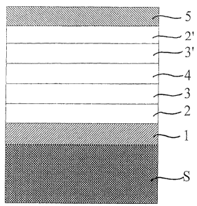
Fig. 1 shows the usual structure of an organic light-emitting diode (OLED). A
base electrode
1 is deposited in a structured manner onto a carrier substrate S, for example
glass or poly-Si.
In the next step, the layer-wise thermal evaporation and separation of a stack
of organic layers
is effected whose properties are specified more precisely further below.
Finally, a cover elec-
trode 5 is deposited, which covers the upper organic layer of the stack
processed beforehand.
At least one of the electrodes is transparent in any case in order to allow
the light emission. In
the case of an organic "bottom-emission " diode where the generated light is
radiated through
the substrate, both the substrate S as well as the base electrode 1 must be
transparent. It is
however necessary that, with an organic "top-emission" diode, the cover
electrode 5 and an
encapsulation of the structural element are adequately transparent. It is also
conceivable that
both sides of the structural element are transparent so that the diode appears
transparent.
It is to be emphasised at this point that both electrodes 1 and 5 can inject
either electrons or
holes, but that no restriction is to be effected with regard to the actual
polarity of the presented
structural element. For this reason, the invention can be implemented in
conjunction with in-
verted (base electrode as cathode) as well as with non-inverted (base
electrode as anode)
structural elements including time-saving and cost-favourable manufacturing
processes.
The non-inverted stack of organic layers comprises five basic components: a p-
type doped
hole transport layer 2, a non-doped intermediate layer on the hole side,
namely an electron
block layer 3, a light-emitting emission layer with k (k=l, 2, 3...) layers, a
non-doped inter-
mediate layer on the electron side, namely a hole block layer 3', and an n-
type doped electron
transport layer 2'.
CA 02543276 2006-04-12
-9-
However, if an inverted structure is selected, then the n-type doped electron
transport layer 2
is followed by a non-doped intermediate layer on the electron side, namely a
hole block layer
3, then the light-emitting emission layer 4 with k (k=1, 2, 3...) layers, the
non-doped interme
diate layer on the hole side, namely an electron block layer 3', and the p-
type doped hole
transport layer 2'.
With regard to the dopants, it is to be noted that acceptor molecules for p-
type doping are se-
lected preferably from the group of the quinones (compare also for this
purpose DE 103 57
044.6). A well known example is F4-TCNQ that is frequently used in order to
dope organic
hole transport layers. This has been elaborately described by Pfeiffer for
example (compare
Appl. Phys. Lett., 73, 22 (1998)). As an alternative, other oxidising
substances are also ap
plied for p-doping, for example FeCl3 (compare J. Endo et al.: Jpn. J. Appl.
Phys. Pt. 2, 41,
L358 (2002)). For n-doping it is standard practice to select elements from the
group of the
alkaline metals (for example Li, Cs) or alkaline earth metals (for example
Mg). However,
molecular donors can also be used.
The stack of organic layers is described as follows in greater detail. In this
case, O1 to 04
designate in general different organic matrix materials. The organic matrix
materials O1 to 04
are partially dopable, selectively by means of n-doping and/or p-doping. At
first, the same
organic matrix material O1 is used for the layers 2 and 3 of the stack. At the
same time, an-
other organic matrix material 02 is used as a matrix for the two layers 2'and
3':
p-doped O1 / O1 / 4 / 02 / n-doped 02
This layer arrangement corresponds to a stack of organic layers with a p-doped
hole transport
layer from the organic matrix material O1, an electron block layer from the
organic matrix
material O1, the emission layer 4, a hole block layer from the organic matrix
material 02 and
an n-doped electron transport layer from the organic matrix material 02. These
embodiment
examples have in common that, for the p-doped hole transport layer and the
adjacent electron
block layer, the same organic matrix material O1 is used and for the n-doped
electron trans-
port layer and the adjacent hole block layer the same organic matrix material
02 is used. The
p-doped hole transport layer and the relevant and adjacent electron block
layer as also the n-
doped electron transport layer and the relevant and adjacent hole block layer
are each made
from the same organic matrix material, where the transport layers have a
doping but the block
CA 02543276 2006-04-12
- 10-
layers do not. For this reason, a doping gradient is formed in each case
within the two ma-
trixes consisting of transport layer and block layer.
In principle, a pin-structure is envisaged where the overall number of the
organic matrix mate-
s rials used in the stack of the organic layers exceeds by not more than two
the number of the
organic matrix materials used for the emission layer. The organic materials)
used for the
emission layer 4 can be fluorescent as well as phosphorescent. The emission
layer can then be
designed as a plain emission layer (k=1 ), where the emission layer consisting
of:
a) O1 or
b) 02 or
c) 03 or
a') a system consisting of matrix Ol :emitter or
b') a system consisting of matrix 02:emitter or
c') a system consisting of matrix 03:emitter.
The designation "matrix Ox:emitter" means that the emission layer is formed
from an organic
matrix material Ox (x=l, 2, ...) and an added emitter material. However, the
emission layer 4
can also be configured as a double emission layer (k=2), where
d) O1 on the hole side and 03 on the electron side or
e) 03 on the hole side and 02 on the electron side or
f) O1 on the hole side and 02 on the electron side or
g) 03 on the hole side and 04 on the electron side are arranged.
The emission layer 4 can be furthermore designed as a double emission layer,
where as or-
ganic matrix material for one or several added emitters the following
selections are made:
d') O1 on the hole side and 03 on the electron side or
e') 03 on the hole side and 02 on the electron side or
f) O1 on the hole side and 02 on the electron side or
g') 03 on the hole side and 04 on the electron side.
Therefore, the organic matrix materials of the transport layers are in each
case identical with
the adjacent block layers or even a component of the emission layer. A
prerequisite for this is,
however, that the organic matrix material O1 (and/or 02) can be doped with
acceptors (do-
nors) and functions at the same time as a barrier for electrons (holes) in the
organic stack,
CA 02543276 2006-04-12
-11-
during which it also allows that holes (electrons) access the emission zone.
An exception are
the embodiment examples c), c'), g) and g') where the organic matrix material
of the emission
layer differs from that of the block layers.
The stated structures are the result of comprehensive examinations and are
substantially sim-
plified compared to the known complex structures as stated, for example, in
the document DE
100 58 587 C2. In addition to this, critical parameters were determined, which
preferably
have the individual materials for a certain function, namely in particular as
doped charge car-
rier transport layer, block layer or emission layer. These parameters are, in
particular, the en-
ergetic positions of the charged and/or excitated conditions of this molecule.
The description
of these parameters is given below.
These examinations were combined with comprehensive test series for the
identification of
materials whose properties enable their application for a plurality of the
required functions.
For the purpose of gaining a more indepth understanding, simulations of OLEDs
were carried
out with a specially developed program. The procedure is described in an
exemplary manner
as follows and the knowledge as well as the design rules derived therefrom are
stated.
The procedure is explained with the example of the hole transport layers
adjacent to the an-
ode. A pin-OLED with Me0-TPD as a hole transport layer, Spiro-TAD as electron
block
layer and TAZ as anode-side emitter matrix are deployed as this is known
(compare He et al.:
Appl. Phys. Lett., 85 (17), 3911 (2004)). An observation of the ionisation
potentials of the
participating substances shows that the barrier for holes during transport of
hole transport
layer to the electron block layer is 0.3eV. The hole injection from the
electron block layer into
the emission layer is effected barrier-free (compare Pfeiffer et al.: Adv.
Mat., 14 (22), 1633
(2002)). The barrier for the injection of holes from the anode into the hole
transport layer is
approximately 0.5 eV. It is known that the anode made of ITO with hole
transport materials
with similar ionisation potential such as Me0-TPD forms ohmic contacts. With
regard to the
potential layers of the participating substances, the anode-side OLED
structure as stated by
He et al. corresponds essentially to the structures, which were reported for
pin-OLEDs with
block layers up to now, in the first instance by Zhou et al. (Appl. Phys.
Lett. 80 (1), 139
(2002)).
CA 02543276 2006-04-12
-12-
In order to realise a plain OLED structure, the number of applied matrix
materials was re
duced. All known realisations of efficient pin-OLEDs use different matrix
materials for the
hole transport layer and the electron block layer. The cause for this is that
the doping capabil
ity of the hole transport layer on the one hand, and the good function of the
electron block
layer on the other, impose very different demands on the properties on these
layers.
At first, the p-doped hole transport layer was made from Spiro-TAD. It was
evident here that
Spiro-TAD can not be adequately doped with the normally used acceptor molecule
F4-
TCNQ. The result is that the contact to ITO is no longer ohmic and light
emission can only be
observed with comparably high operating voltages. Furthermore, the electron
block layer was
manufactured from non-doped Spiro-TTB (2,2',7,7'-Tetrakis-(N,N-ditolylamino)-
9,9'-
spirobifluorene), whereas the hole transport layer consists of p-doped Spiro-
TTB. With refer-
ence to the ionisation potential and the doping capability with F4-TCNQ, this
material is to be
regarded as being equivalent to Me0-TPD. It was discovered here that an ohmic
contact to
the ITO is however formed but that, on the other hand, minor efficiencies for
light emission
occur due to the high barrier for hole injection into the emission layer used
here. The cause is
quenching effects resulting from exciplex formation and luminescence quenching
at the ac-
cumulated holes at the boundary surface between block layer and emission
layer. Further-
more, other hole transporting materials with a higher ionisation potential
than Me0-TPD, but
with a lesser ionisation potential than Spiro-TAD, were used as p-doped hole
transport layer
and as electron block layer. It was discovered here that none of the
materials, in the doped
case on the one hand, forms ohmic contacts with ITO and at the same time, on
the other hand,
does not produce any quenching effects in the emission layer. Electrical
simulations showed
that a barrier of approximately 200meV between two organic layers does not yet
substantially
influence the current transport, but that at about 400meV considerable
accumulation build-up
already occurs.
It was recognised that the problem can be solved if acceptor molecules
stronger than F4-
TCNQ are used. In this way, materials with a higher ionisation potential than
Me0-TPD or
Spiro-TTB could also be doped, and even Spiro-TAD under certain circumstances.
However,
acceptor molecules stronger than F4-TCNQ were unknown in the state of the art
up to the
present. An acceptor molecule stronger than F4-TCNQ was used, which is 2-(6-
dicyanomethylene-1, 3, 4, 5, 7, 8-hexafluoro-6H-naphtalene-2-ylidene)-
malononitrile and
which is designated in the following as SAM (compare Fig. 8). It was
discovered that a dop-
CA 02543276 2006-04-12
-13-
ing of Spiro-TAD was actually successful in that way. It was possible in that
way to form the
doped hole transport layer and the electron block layer from the same material
(Spiro-TAD)
and at the same time to ensure a good injection from the anode formed with ITO
and minor
quenching effects at the boundary surface to the emission layer.
Finally, Spiro-TAD was used also as a matrix material for red triplet
emitters, and this made
possible a further simplification of the OLED (compare application example a'
above).
In a next step, it was examined to what extent one or several block layers are
necessary at all
with the novel layer structures. Block layers can be deployed in order to
avoid negative
quenching effects. Up to now, all efficient OLEDs with pin-structure have two
block layers,
in each case one on the cathode side and one of the anode side.
An important factor for the understanding of the quenching effects is the
knowledge of the
location of the recombination zone of the pin-OLEDs. As excitons in organic
layers have as a
rule limited diffusion length in the magnitude of lOnm, there is only an
appreciable exciton
density in the structural element also only within the diffusion range. As a
rule, quenching
effects are attributable to short-range alternating effects with excitons. For
this reason, the
source of these effects must be within the diffusion zone around the
recombination area in
order to noticeably worsen the efficiency. Little is known about the location
of the emission
zone in pin-OLEDs. Experiments with the so-called "doped slab " technique were
carried out
for conventional OLEDs. In this case, various OLEDs were manufactured with the
same
structure for which, in each case, a very thin exciton sensor layer was
introduced at various
positions in the emission layer. The luminescence signal of the exciton sensor
layer is as-
sumed as being proportional to the exciton density locally. In conventional
OLEDs, a differ-
ence was made between so-called electron-rich and/or electron-poor structures.
In the first
case, the recombination zone is primarily on the anode side of the emission
layer, whereas in
the second case it is on the cathode side. The cause for electron surplus
and/or electron short-
age is, in addition to the differently large mobility for electrons and holes,
the barriers for the
charge carrier injection in particular.
Furthermore, another method was selected for the examination of pin-diodes,
namely the
comparison of OLEDs with a variation of the thicknesses of the transport
layers with an opti-
cal model. This variation leads to a variation of the distance of the emission
layer from the
CA 02543276 2006-04-12
- 14-
reflecting electrode, which is frequently a cathode. Displacements in the
emission spectrum
and a variation of the decoupling efficiency and the emission characteristics
result because of
interference in the originating thin layer system.
The comparison of experiment and optical simulation for various locations of
the emission
zone in the stack enables the determination of their actual location in the
structural element. In
the result of these experiments it was discovered that, for pin-OLEDs, the
location of the
emission zone is established not by barriers for load carrier injection but
rather primarily be-
cause of the relation of movements for electrons and holes in the emission
layer. The differen-
tiation between electron-poor and electron-rich OLEDs therefore loses its
original signifi-
cance. If the electron mobility is prevailing in relation to the hole mobility
in a concrete emit-
ting layer, the recombination takes place in the vicinity of the electron
block layer. This
means that, in this case and with sufficient thickness of the emission layer,
the exciton density
at the hole block layer is very small. Quenching effects at this boundary
surface are thus in-
significant, and the hole block layer is not required. By way of analogy, the
electron block
layer is not required with a dominating hole mobility. For examination
purposes, OLEDs
were manufactured (see below) where no non-doped intermediate layer is
inserted between
the hole transport layer and the emission layer with a dominating hole
mobility. Strong
quenching effects are normally expected for such OLEDs as the requirements for
practically
all types of luminescence quenching at the boundary surface are established,
namely the pres-
ence of the charged dopant anions, the accumulation of a high hole density due
to a high bar-
rier to the emission layer and the energetic acceptance of exciplex formation.
In fact, it was
observed that the efficiency of these structures is very high. A surprising
result that can, how-
ever, be explained with the help of the reasons stated above.
Properties with regard to the energy levels of the participating materials are
compiled as fol-
lows for the manufacture of efficient but uncomplicated structured OLEDs.
As the available acceptors (donors) have a limited doping strength (according
to electron of
finities and/or ionisation potentials), maximum values for the ionisation
potential (minimal
values for the electron affinity) result therefrom for the organic matrix
materials O1 to 04. In
order to additionally serve as an electron (hole) barrier, there are
additionally maximum val-
ues for the electron affinity (minimal values for the ionisation potential) of
the organic matrix
materials.
CA 02543276 2006-04-12
-15-
The commercially available acceptor molecule F4-TCNQ can be used as a p-dopant
in a hole
transport material. It has an electron affinity EA(A) of approximately 5.3 eV
(estimation from
cyclovoltammetry). For a matrix O1 doped with F4-TCNQ, there is therefore the
requirement
that the ionisation potential IP(O1 ) (estimated from cyclovoltammetry) is 0.5
eV larger as a
maximum. Caesium atoms are frequently used as donors. Atomic caesium has an
ionisation
potential of 3.9 eV. Based on a strong alternating effect between matrix and
dopant (complex
formation) it is however possible to dope matrix materials with a far smaller
electron affinity.
The well known matrix material BPhen has, for example, an electron affinity
between 3.0 eV
(estimation from ionisation potential and optical band gap) and 2.4 eV
(estimation from
cyclovoltammetry). However, it can be expected that, for materials with an
electron affinity
smaller by 0.5 eV, a doping effect with caesium cannot be achieved. For a
molecular n
dopant, and based on the details for p-dopants, in the result the electron
affinity of the matrix
EA(02) shall not drop below the value, reduced by 0.5 eV, of the ionisation
potential of the
donor IP(D).
Consequently, the following relationships result from the requirement of the
doping capabil-
ity: IP(Ol)<EA(A)+0,5 eV and/or EA(02)>IP(D)-0.5 eV. The following applies in
the case
of doping with caesium: EA(02)>1.9 eV.
For the fulfilment of the barrier characteristics, the requirement on the
EA(O1 ) and/or IP(02)
results from the potential levels of the emission layer. Electrons that move
energetically in the
level of the electron affinity of the emission layer EA(E) shall only access
the layer O1 at a
low rate. The result is subsequently: EA(O1 )<(E)-0.2 eV. At the same time,
holes that move
energetically in the level of the ionisation potential of the emission layer
IP(E) shall only ac-
cess the layer 02 at a low rate: IP(02)>IP(E)+0.2 eV. Attention is drawn again
here to the
fact that the conditions for barrier characteristics do not have to be
fulfilled in every OLED
stack. If the emission zone is near to the hole transport layer, there is
frequently no necessity
that the layer adjacent to the emission stack on the cathode side represents a
barrier for holes.
The same applies for an OLED with an emission zone near the electron transport
layer, in that
there is frequently no necessity that the layer adjacent to the emission stack
on the anode side
represents a barrier for electrons.
CA 02543276 2006-04-12
-16-
In order to obtain an efficient injection of charge carriers from the
individual charge carrier
transport layers and/or the block layers into the emission layer, it is to be
demanded that the
barriers to be overcome by the charge carriers in this case are not too large,
meaning, smaller
than 0.5 eV. It is emphasised here that, where higher barriers are concerned,
an increase of the
operating voltage is to be expected on the one hand. On the other hand, a
reduction of the ef
ficiency of the emission can also occur if the accumulated charge carrier
density at the bound-
ary surface to the emission layer leads to an increase of the non-radiating
recombination of
excitons in the emission layer. On the whole, these criteria result: IP(O1
)>IP(E)-0.5 eV and
EA(02)<EA(E)+0.5 eV.
It is at first surprising that, on the one hand, an efficient charge carrier
injection into the emis-
sion layer can take place if the barrier is up to 0.5 eV, but on the other
hand the performance
of the diode is not detrimentally affected if the barrier for the injection
from the emission
layer into the block layer is only 0.2 eV. This is attributable to the fact
that the desired recom-
bination of electrons and holes occurs within the emission layer as a
competing process to the
charge carrier loss into the block layers. For this reason, the residence time
of the charge car-
riers in the vicinity of the barrier in the emission layer is significantly
shorter than in the case
of a unipolar charge transport layer. This leads to a limitation of the charge
carrier losses also
for comparably small barriers. Material examples are: BPhen can be doped with
caesium, but
at the same time can also be used as a hole block layer and matrix for the
green emitting
molecule Ir(ppy)3.
On the hole side, Spiro-TAD offers the possibility at the same time for p-
doping and as elec-
tron block layer and functions additionally as a matrix for red emitters also,
for example.
In the following, further embodiment examples for layer arrangements in the
stack of organic
layers are explained in greater detail for an organic pin-type light-emitting
diode. 0l to 04
again designate generally different organic matrix materials.
m) p-doped O1 / O1 / Ol :emitter / 03 / n-doped 02
n) p-doped Ol / 03 / 02:emitter / 02 / n-doped 02
As previously explained in an exemplary manner, such an arrangement leads to
the formation
of a kind of uniform transition on only one side of the emission layer in each
case which is
shown in the embodiments below as an underlined text. A uniform transition in
the sense of
CA 02543276 2006-04-12
-17-
the invention is a layer sequence that is formed from a charge carrier
transport layer up to the
emission layer by means of a uniform matrix. If the emission zone is in the
middle of the
emission layer, the block layers can be deleted. This leads to the structures
m*) and n*):
m*) p-doped O1 / O1:emitter / n-doped 02
n*) p-doped O1 / 02:emitter / n-doped 02
After the stepwise adaptation of the layer materials (compare embodiment
examples o), o*),
p), p*), q) below), the structures of the embodiment examples r), s), t) can
be realised where
the HOMO-levels and the LUMO-levels perfectly assimilate because the same
matrix mate-
rial is used all the way through in all layers.
o) p-doped O1 / O1 / Ol :emitter / 02 / n-doped O1
o*) p-doped O1 / Ol :emitter / 02 / n-doped O1
p) p-doped Ol / 02 / Ol :emitter / n-doped O1
p*) p-doped O1 / 02 / Ol :emitter / Ol / n-doped O1
q) p-doped O1 / 02 / Ol :emitter / 03 / n-doped O1
r) p-doped O1 / O1 / Ol :emitter / n-doped O1
s) p-doped Ol / Ol :emitter / O1 / n-doped O1
t) p-doped O1 / Ol :emitter / n-doped O1
Furthermore, the emission layer can exist in the structures of the embodiment
examples m) to
t) even out
of only one
of the materials
O1, 02 or
03:
m') p-doped O1 / O1 / 03 / n-doped
02
m") p-doped O1 / O1 / n-doped
02
n') p-doped O1 / 03 / 02 / n-doped
02
n") p-doped O1 / 02 / n-doped
02
o') p-doped O1 / O1 / 02 / n-doped
O1
p') p-doped O1 / 02 / O1 / n-doped
Ol
q') p-doped O1 / 02 / O1 / 03
/ n-doped O1
r'= s'= t') p-doped O1 / Ol / n-doped
O1
All layer combinations listed above can be used in inverted and in non-
inverted OLEDs, de-
pending on the polarity of the base and cover electrode. The structures in the
embodiment
examples m) to t') all comprise only one emission layer from one single matrix
material,
therefore k = 1 applies. By way of analogue, the simplifications named apply
however also
CA 02543276 2006-04-12
- lt~ -
for the structures in the embodiment examples m) to q) and m') to q') for k =
1, 2, 3... Particu-
larly where white OLEDs are concerned, k is frequently larger than 1 as the
white spectrum is
made up of constituents of different colours.
The greatest challenge during the construction of an OLED with the same matrix
for p- and n-
doping is finding a matrix material that can be doped with a p- as well as
with an n-dopant, so
that it can be used in the hole and the electron transport layer. For the case
that this material is
also to be used as emitter or emitter host, its energy gap between HOMO and
LUMO must be
in a range that enables electrons and holes to penetrate the emission zone and
to recombine
there is a radiating manner. The explained details for the orbital levels of
the matrix result
direct from the considerations stated above according to the identity of the
organic matrix
materials O1 and 02. Phthalocyanine, for example ZnPc and CuPc, phorphyrine,
for example
ZnOEP, PtOEP or iridium (III) tris (1-phenylisoquinoline) are materials that
have been used.
In the following, reference is made to the Fig. 2A to 2C. The most
uncomplicated structure
can be realised by a three-layer system which is shown above, for example, as
embodiment
r'). In principle, HOMO and LUMO levels match perfectly at every boundary
surface if the
same matrix material is involved on both sides of the boundary surface. That
means that there
is absolutely no energy barrier in such an OLED within the organic, neither
for the electrons
on their route through the LUMO nor for the holes on their route through the
HOMO.
In order to obtain low operating voltages of the OLED, both charge carrier
transport layers are
doped. This presupposes that the matrix material can be p-doped as well as n-
doped. The bal
ance of the two charge carrier types which must be balanced out for a high
current efficiency
can be set by way of the degree of the p- and n-doping.
The greatest advantage of this structure is its uncomplicated processing. In
this case, however,
charge carrier balance must be set. This can namely also depend on the applied
voltage and,
subsequently, on the brightness. A further parameter that has to be taken into
account is the
exciton diffusion length. If it is so large that the excitons can diffuse out
of the emission zone,
that will also reduce the efficiency.
As required, one (compare Fig. 2B and 2C; embodiment examples o*), o'), p),
p')) or even
two (compare embodiment examples o), q), p*) and q')) block layers must be
introduced,
CA 02543276 2006-04-12
-19-
which restrict the holes and electrons in the emission layer. In this case,
the energy difference
of the LUMOs / HOMOs of the layer 3 / 3' and the emission layer 4 (compare
Fig. 1 ) acts as a
barner for the electrons / holes with a non-inverted structure. This applies
by analogy for an
inverted structure. In this way, charge carriers are accumulated in the
emission layer, a fact
which again results in efficient light generation.
In OLED structures there are occasionally further layers that are introduced
between the con-
tacts and the layer structures described here. These layers can, for example,
serve the im-
provement of the charge carrier injection or a better adhesion of the contact
at the organic
layers. It is understood that the described layer structures also concern such
OLEDs, which
include this type of layers additionally to the layer stack described here.
This refers not only
to coloured but also to white OLEDs.
Particularly attractive is the simplification according to the invention of
the layer stack for the
use in so-called "stacked" OLEDs. "Pin-stacked" OLEDs is normally understood
to mean
OLEDs with several pin-layer sequences on top of each other. These OLEDs
enable high cur
rent efficiencies and the mixing of colours with the use of variously emitting
emission stacks
in the individual sub-pin-OLEDs. Particularly with these OLEDs which can
consist of ten or
more layers, the saving of each individual layer is a guarantee for higher
production yield and
more cost-favourable manufacture.
Full-colour displays with red, green and blue sub-pixels are a significant
application for
OLEDs. Pin-structures are used for this application also, where the attempt is
made to deposit
in a structured manner only the emission layer stack and/or the emission layer
by means of a
shadow mask in order to obtain the three differently coloured sub-pixels
types. All other lay-
ers, meaning for example the transport and block layers, are to be jointly
deposited for the
three colours. However, this means for example that a block layer on the
electron side can
only then be dispensed with if the OLED simplified in this way functions
equally well for all
three colours. By means of the knowledge gained, the emitter matrixes can now
be specifi-
cally selected in such a way that the same blocker can be dispensed with for
all three colours.
For example, one could select emitter matrixes for all three colours, which
predominantly
transport holes and subsequently, depending on the circumstances, dispense
with the electron
block layer.
CA 02543276 2006-04-12
-20-
In the following, and supplementary to the embodiments already described,
further examples
for the realisation of the simplified structures are described. Here, SAM was
used as a p-
dopant.
i) Example for a structure according to the embodiment c')
A red bottom-emitting OLED was processed on ITO with Spiro-TTB as organic
matrix mate-
rial for the hole transport layer and as electron block layer. On the electron
side, a combina-
tion of non-doped and Cs-doped BPhen was implemented. A reflective aluminium
cathode
was deposited as a cover electrode. The emission layer consists of the emitter
system
NPD:Iridium (III) to (2-methyldibenzo[fh]-quinoxaline)(acetylacetonate). The
characteristic
data are shown in the Fig. 3A and 3B. At only 2,6V, light with a brightness of
100 cd/m2 and
an efficiency of 6.6 lm/W is emitted.
ii) Example for a structure according to the embodiment a')
In contrast to the previous example, Spiro-TAD is applied here as a matrix for
the hole trans-
port layer, as intermediate layer 3 and as matrix for the emitter dye iridium
(III) tris (1-
phenylisoquinoline). All other layers were grown on by analogy with the
previous example.
The characteristic data are shown in the Fig. 4A and 4B. The performance
efficiency reaches
5.7 Im/W with a brightness of 100 cd/m2 and an operating voltage of 3,7V.
iii) Example for a structure according to the embodiment n)
A uniform transition on the electron side is realised with the help of a BPhen-
matrix that is
doped with Cs in order to ensure a high n-conductivity. BPhen is furthermore
used as a hole
block layer and as matrix material for the green-emitting emitter Ir(ppy)3. On
the p-side and
with SAM, p-doped Spiro-TTB was deposited on transparent ITO and onto this non-
doped
Spiro-TAD as electron block layer, restricting the electrons in the emission
zone, was sepa-
rated. The characteristic data were shown in the Fig. 5A and SB. Steep current-
voltage charac-
teristic curves were measured. 1000 cd/m2 was obtained at an operating voltage
of 2.75V and
a performance efficiency of 22.2 lm/W.
iv) Example for an individual structure according to the embodiments o'), p'),
r')
CA 02543276 2006-04-12
-21 -
The red-emitting material iridium (III) tris (1-phenylisoquinoline) is a
suitable organic matrix
material, which shows an increased conductivity with doping with acceptors as
well as with
donors. Three OLEDs based on this matrix material were built, namely a diode
without block
layers, a diode with MeT-TPD that was applied as an electron block layer (EB)
and a diode in
the 4,7-diphenyl-2,9-dicyano-1,10-phenanthroline(bathophenanthroline) as a
hole block layer.
Cs was used as an n-dopant. Characteristic data of these diodes are shown in
the Fig. 6 and 7.
All samples show a good diode characteristic. The diode with EB emitted red
light of a
brightness of 100 cd/m2 at 2,9 V. It is clearly evident that the luminance of
the diodes is in
creased with the use of the block layers.
On the whole and with the described arrangements of organic layers, new
configuration op-
tions with reference to the interaction between block layer and charge carrier
transport layer
and emission layer are created. Proceeding on the basis of simplified OLED
structure, a
method was furthermore created as to how OLEDs could be significantly and more
easily
processed. The point of initiation is the use of the same organic matrix
material for several
layers, for example as matrix material for the p-dopant, as electron blocker
and as matrix ma-
terial for the emission layer. For the manufacture of such layer arrangements,
one or several
evaporation sources for further matrix materials can be saved, which have to
be vapour-
deposited in known processes. In addition, it is enabled that the source for
the matrix material
can be continually operated. At first, a co-evaporation of the matrix with the
p-dopant takes
place (vapour deposition of the hole transport layer). Then the closure of the
source of the p-
dopant is closed and only the matrix is evaporated further (vapour deposition
of the electron
block layer). Then the closure for the emitter dye is opened and the emitter
dye is co-
evaporated together with the matrix material (vapour deposition of the
emission layer). This
procedure saves time for the heat-up and heat-down of the source for the
matrix material and
saves costs as well because only one source is used for the matrix material.
In summarising, the invention is based on the knowledge that the plurality of
criteria that has
to observed with the selection and the combination of organic matrix materials
for the charge
Garner transport, the charge carrier blockage and the light emission in
organic pin-type light-
emitting diodes does not necessarily lead to a situation where these matrix
materials have to
be different with regard to pairing. For example, one and the same organic
matrix material,
for example Spiro-TAD, can also be used as a matrix material for a hole
transport layer in
CA 02543276 2006-04-12
-22-
addition to its known use as block material, even though the criterion of
doping capability and
the criterion of the small barrier for the injection of holes into the
emission layer are in oppo-
sition to one another. Here, new types of acceptors such as SAM, for example,
are incorpo-
rated, which considerably expand the class of the p-dopable matrixes. In
particular, materials,
which were formerly used exclusively as block material can now also be used as
p-doped hole
transport material.
It was furthermore recognised that, in embodiments, the use of a block layer
is dispensable for
a charge carrier type, particularly if the mobility of this charge carrier
type exceeds the mobil-
ity of the other charge carrier type in such a way that the emission zone is
located far away on
the opposite side of the emission layer. In this case it is also possible to
select the same matrix
material for the emission layer as for the transport layer of this highly
mobile charge carrier
type. For example, in the case of an emission layer comprising TCTA:Ir(ppy)3,
an electron
blocker consisting of Spiro-TAD for example can be dispensed with, even though
in the state
of the art such structures with Spiro-TAD or similar are stated at all times,
for example in He
et al.: Apply. Phys. Lett., 85 (17), 3911 (2004)).And in this case also, the
emission layer and
the hole transport layer can consist of the matrix material Spiro-TAD. This is
surprising as the
organic pin-type light-emitting diode as such has been known for more than ten
years.
Furthermore, the knowledge was gained that it is possible in embodiments to
use the one and
the same material as matrix for the electron as well as the hole transport
layer. Here, the con-
ditions of doping capability for both charge carrier types, on the one hand,
and the condition
of the low barriers for charge carrier injection into the emission layer as
well as the condition
of exclusion of the exciplex formation, on the other hand, are in opposition.
It was recognised
that acceptor and/or donor compounds can be selected, which are strong in
order to ensure the
charge carrier injection into a red radiating emission layer.
Despite the fact that, with the described arrangements of organic layers, the
entire structure of
the OLED was significantly simplified, highly efficient structural elements
are still being
manufactured. The cause in this case is the uncomplicated injection of the
charge carriers
from the electrodes into the organic layer arrangement and the almost loss-
free transport of
the charge carriers through the transport layers based on the doping as well
as the efficient
recombination in the emission zone.
CA 02543276 2006-04-12
-23-
The features of the invention as disclosed in the description given above, as
well as in the
drawing and the Claims can be of significance both individually as well as in
random combi-
nation for the realisation of the invention is its various embodiments.