Note: Descriptions are shown in the official language in which they were submitted.
CA 02543396 2006-04-21
WO 2005/123227 PCT/US2004/018206
-1-
1
2
3
4
6
7
8
9
to METHOD FOR MANIPULATING MICROSCOPIC PARTICLES AND
11 ANALYZING
12 THE COMPOSITION THEREOF
13
14 Fatent Application of
Thomas M. Moore and John M. Anthony
16
1 ~ TECHNICAL FIELD
18 The invention relates to techniques for removing and analyzing microscopic
19 particles from a sample surface, particularly from semiconductor samples.
2o BACKGROUND
21 In the semiconductor industry, unexpected particles due to contamination
will
22 cause yield loss during the manufacturing process. Since a major focus of
this industry is
23 aggressive reduction in feature size for pattern line widths, the minimum
size of particles
24 that can cause performance loss also decreases rapidly. A reasonable
estimate for a
"killer defect" size is that greater than one-third the size of the smallest
feature on the
26 semiconductor wafer.
27 Although semiconductor manufacturing is performed in clean rooms with
28 stringent particle standards, unexpected contamination will occur due to
sources such as
29 moving parts, human presence, gas condensation, and chamber wear. Control
and
removal of these particles is a continuous process. In many cases, removal of
the source
31 of particles requires an understanding of their origin. Many of these
particles or defects
32 are too small for detection in a general purpose optical inspection
microscope, so higher
33 resolution methods are required, using charged-particle microscopes, such
as scanning
CA 02543396 2006-04-21
WO 2005/123227 PCT/US2004/018206
-2-
1 electron microscopes (SEM), transmission electron microscopes (TEM),
scanning Auger
2 microprobes (SAM), or focused ion beam (FIB) instruments, are required.
3 Even an image of the particle is usually insufficient to trace the origin of
the
4 particle, and more information is required. Elemental composition is
valuable in
identifying the defect. This can be done in various ways using the charged-
particle
6 systems mentioned above. Unfortunately, most of the analytical methods are
limited by
7 background signals from the environment of the particle.
8 Throughput is also a critical parameter in semiconductor manufacturing.
9 Existing strategies for compositional analysis of particles on a
semiconductor wafer, for
l0 example, usually require removal of the wafer from the fabrication area for
off line
i i analysis using methods such as those described below. Removal from the
line severely
12 reduces the throughput of the manufacturing process.
13 Particle identification on sample surfaces using electron-beam based
identification
14 is complicated by the size of the particle relative to the electron
penetration depth, and by
the nature of surrounding materials in the sample. As an electron beam
interacts with
16 bulls solid materials, it expands to fill a teardrop-shaped volume as it
loses energy. As
17 the primary beam interacts with atoms in this volume, it generates low
energy Auger
i8 electrons and X~rays that are characteristic of the elements involved.
19 The particular X-ray line generated will depend on the atomic number of the
2o element, the energy of the electron during the interaction; and other
factors. When
21 trying to identify an unknown particle using conventional Energy-dispersive
X-ray
22 Spectrophotometry (EDS), the energy of the electron beam must be large
enough to
23 generate inner-shell X-rays from all possible relevant elements, which, for
semiconductor
24 applications, may include elements of high atomic number such as tungsten.
Unfortunately, this energy results in a penetration depth that may be much
larger than the
26 particle of interest, resulting in X-ray generation from the sample
surface. These X-rays
27 interfere with any signal from the particle, making unique identification
of the particle
28 material difficult. Conventional strategies for solving this problem
involve either
29 resolving the X-ray lines of different elements, or reducing the energy of
the exciting
3o electron beam.
31 For example, it is possible to detect and analyze electron-beam generated X-
rays
32 from a particle by measuring the intensity and diffraction angle of the X-
rays diffracted
33 by a reference crystal, or Wavelength Dispersive X-ray Spectrometry (WDS).
One
CA 02543396 2006-04-21
WO 2005/123227 PCT/US2004/018206
-3-
1 chooses the crystal atomic spacing to deflect (with very high resolution) X-
rays of a
2 given energy, thus allowing separation between X-ray lines of different
elements. This
3 method has higher energy resolution than EDS but much slower throughput. In
addition,
4 if the particle could be, as it often is, of the same composition as the
sample surface, this
method will not uniquely determine the particle composition.
6 Other solutions involve reducing the energy of the primary electron beam to
7 guarantee the activated volume is less than the volume of the particle of
interest. This
8 reduction in primary electron-beam energy results in characteristic X-rays
of much lower
9 energy (M or L shell X-rays, rather than K shell). Conventional cooled
semiconductor-
based detectors use the generation and collection of electron-hole pairs as a
measure of
11 the energy of the ionizing radiation (a few eV for each electron-hole pair,
depending on
12 the detecting material). A reduction in the X-ray energy therefore leads to
a reduced
13 number of electron-hole pairs and reduced sensitivity to the particle
material. In addition
14 the resolution of these detectors is governed by the statistics of the
electron-hole
generation process, and reducing the energy of the detected X-ray often leads
to
16 ambiguous identification of the element of interest. X-ray micro-
calorimeter methods
17 have been used to detect these weak X-ray signals, using heat transferred
to the detector
18 rather than the generation of electron-hole pairs. This process does allow
measurement
19 of small X-ray energies, but micro-calorimeter instruments are expensive,
have
2o complicated cooling requirements, and are slow compared to other methods.
Also, the
21 electron beam must be kept smaller than the smallest dimension of the
particle of interest,
22 rendering the method impractical for small, unsymmetrical particles.
23 Scanning Auger microprobe analysis also uses an electron beam to irradiate
a
24 particle of interest, but rather than detecting any X-rays generated it
focuses on the
detection of Auger electrons ejected from the atoms of the material. These
Auger
26 electrons come from outer shells and have relatively low energies. The
Auger electron
27 energies from a material produce a pattern that is characteristic of each
element in the
28 material, and the shape and exact energy of the Auger transitions provide
information on
29 the chemical bonding of the elements in the material (such as, phase or
compound
information). The escape depth of these electrons is quite small (a few nm),
so Auger
31 analysis focuses mainly on the surface of a sample. This is an advantage
for the analysis
32 of small diameter particles (<10 nm). For the analysis of larger particles,
one can
33 generate depth profiles by using an ion beam to sputter through the
particle and take
CA 02543396 2006-04-21
WO 2005/123227 PCT/US2004/018206
-4-
1 periodic measurements, but this is inherently destructive of the surrounding
sample due
2 to ion milling in the SAM, and requires background analyses on the sample
near the
3 location of the particle. Auger analysis is typically more sensitive to
light elements than
4 standard EDS analysis, making it more suitable to identify organic
materials. However,
to improve counting statistics, high electron beam currents are typically
employed. This
6 exaggerates the issues of thermo-mechanical drift and drift due to
electrical charging of
7 the sample. This means that operating the SAM in the "spot mode," with the
electron
8 beam positioned on the particle, involves a risk that over time the electron
beam spot will
9 drift onto the sample that surrounds the particle. And the use of a raster
pattern for the
io electron beam will be more tolerant of drift for keeping the beam on the
particle, but will
i i involve significant contamination of the results with signal from the
surrounding material.
12 In either case, background contamination of the Auger results is a serious
issue, and
13 Auger analyses of the surrounding material are required to uniquely
identify the signal
14 from the particle. The acquisition of background analyses reduces
throughput and
inherently damages the sample.
16 TEM can often be used for analysis of particles in or on surfaces. There
are a
17 variety of methods for isolating the particle for analysis, including
replication, lift-out or
is cross sectioning the area of interest. These methods all destroy the sample
surface and
19 must be done off line, thereby increasing cost and cycle time.
2o Moving the particle from the first sample surface to a more controlled
21 environment for testing can dramatically improve the chance of success and
throughput
22 for elemental identification with either EDS or Auger analysis. A critical
part of this
23 process is the strategy for moving the particle. This disclosure describes
a novel method
24 for removing a particle of interest from a sample surface, transporting
that particle to a
second sample surface with a controlled X-ray or Auger background, and
performing
26 electron beam-induced X-ray analysis or Auger electron analysis there,
using any of the
27 methods discussed above. This eliminates the requirement that the analyzing
technique
28 have high spatial resolution, although a technique with high spatial
resolution, such as
29 EDS analysis in the SEM and SAM analysis, is generally preferred. For
example,
3o techniques without high spatial resolution that could be successfully
applied to the
31 situation of a particle on a reduced or non-interfering background include
X-ray
32 Photoelectron Spectroscopy (XPS) and X-ray Fluorescence analysis (XRF),
which may
33 offer an advantage in unique and specific situations.
CA 02543396 2006-04-21
WO 2005/123227 PCT/US2004/018206
-S-
1 The proposed method for particle manipulation and EDS X-ray analysis can be
2 done in-line on existing wafer-manufacturing tools. An in-line procedure
using existing
3 manufacturing and inspection tools represents a significant reduction in
cycle time for
4 contamination removal. SEM is a routine method for wafer inspection, and
analytical
methods using the electron beam in an SEM system provide a substantial
throughput
6 advantage over the off line strategies.
7 Although this disclosure primarily illustrates the use of the novel
technique to
8 manipulate and examine particles that are contaminants in the context of
semiconductor
9 manufacturing, the reader should note that the term "particle" may be taken
to include
objects that may not be contaminants in other environments, such as chemical
deposits,
0 11 biological material, or micro-mechanical machines. In the latter cases,
the novel methods
12 of manipulation described in this application may be applied to manipulate
these objects
13 generally, for purposes other than electron-beam X-ray analysis or Auger
electron
14 analysis.
DRAWINGS
16 Figure 1 shows the steps of attaching a particle to a micro-manipulator
probe and
17 removing the particle to a second surface for analysis.
18 Figure 2 shows three other methods of attaching a particle to a micro-
19 manipulator probe.
2o Figure 3 shows the process of modifying electrostatic forces by bombardment
21 with polarizable molecules.
22 Figure 4 shows the method of simultaneously viewing a particle and
modifying
23 the charge state of the particle.
24 Figure 5~ shows several methods for fixing a particle to a second surface
for
analysis.
26 Figure 6 shows the analysis of a particle while the particle is fixed to
the tip of a
27 micro-manipulator probe.
28 Figure 7 shows the process of analyzing the composition of a particle
removed to
29 a second surface for analysis.
SITMMARY
31 We disclose a method for analyzing the composition of a microscopic
particle
32 resting on a first sample surface. Usually, the particle will be a
contaminant in a
33 semiconductor processing system, although the method is not limited to
those
CA 02543396 2006-04-21
WO 2005/123227 PCT/US2004/018206
-6-
1 circumstances. The method comprises positioning a micro-manipulator probe
near the
2 particle; attaching the particle to the probe; moving the probe and the
attached particle
3 away from the first sample surface; positioning the particle on a second
sample surface;
4 and, analyzing the composition of the particle on the second sample surface
by energy-
dispersive X-ray analysis, Auger microprobe analysis or any other suitable
analytical
6 technique. The second surface has a reduced or non-interfering background
signal
7 during analysis, relative to the background signal of the first surface. (We
call such a
8 reduced or non-interfering background signal a "controlled" background
signal in the
9 claims.) We also disclose methods for adjusting the electrostatic forces and
DC
l0 potentials between the probe, the particle, and the sample surfaces to
effect removal of
11 the particle, and its transfer and relocation to the second sample surface.
These include
12 adjusting electrostatic forces to create an attractive force between the
probe and particle.
13 Adjustment of the electrostatic forces may include locally adjusting the
energy or
14 intensity (intensity means beam current for electron and ion beams) of an
electron beam,
ion beam or photon beam incident on the individual components of the sample
system,
16 which includes the probe tip, particle and first sample surface, to create
an electrostatic
17 attraction between the particle and probe tip, or an electrostatic
repulsion between the
18 particle and the first sample surface. This procedure is reversed to
transfer the particle
19 from the probe tip to the second sample surface.
The second sample surface may be the probe tip itself. In this case the probe
tip
21 is composed of a controlled background material. Due to the possibility of
transmission
22 of the energetic beam through a tiny particle, or scattering of the
energetic beam onto the
23 underlying surface, it may be necessary to translate the probe tip with the
particle
24 attached over a surface composed of a controlled background material, or
alternatively
translate such a controlled background surface beneath the probe tip with the
particle
26 attached. In this description, "under" and "beneath" refer to the side of
the particle
27 opposite the side on which the energetic beam is incident (i.e.: the
transmitted side).
28 DETAILED DESCRIPTION
29 The analysis of microscopic particles, particularly in semiconductor
manufacturing, is typically done inside a Scanning Electron Microscope (SEM),
Focused
31 Ion Beam (FIB) instrument, or Scanning Auger Microprobe (SAM). The FIB
instrument
32 may be either a single-beam model, or a dual-beam (both SEM and ion beam)
model.
33 Typical FIB instruments are those manufactured by FEI Company of Hillsboro,
Oregon,
CA 02543396 2006-04-21
WO 2005/123227 PCT/US2004/018206
_7-
1 as models 200, 235, 820, 830, or 835. The probe (120) referred to below is a
2 component of a micro-manipulator tool attached to the FIB instrument with
vacuum
3 feed-through. A typical such micro-manipulator tool is the Model 100
manufactured by
4 Omniprobe, Inc. of Dallas, Texas. Typical SAM instruments include the JAMP-
7810
and JAMP-7830F manufactured by JEOL USA, Inc. of Peabody, Massachusetts.
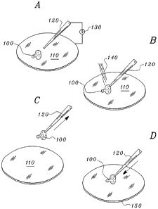
6 Figure 1 depicts the general setup for particle manipulation and analysis.
Fig. lA
7 shows a particle (100) of interest resting on a first sample surface (110).
A micro-
8 manipulator probe (120) is positioned near the particle (1d0). The probe tip
can be
9 electrostatically charged relative to the particle and the first sample
surface.
Alternatively, a voltage source (130) may be connected between the probe (120)
and the
11 first sample surface (110). The local electrostatic charge on the particle
can be modified
12 by the irradiation of the particle by a charged particle beam. Figs. 1 B
through 1 D show,
13 respectively, the irradiation of the particle (100) and first sample
surface (110) by
14 photons or a charged-particle beam (140) to cause attachment of the
particle (100) to the
probe (120), the removal of the probe (120) and attached particle (100) from
the first
16 sample surface (110), and the deposition of the particle (100) on a second
sample surface
17 (150) for analysis. The drawings are not to scale.
18 Attaching the particle to the probe
19 Strong electrostatic forces exist on particles in a vacuum. The presence of
static
charges on the particle (100) and the probe (120) leads to the creation of
image charges
21 on the opposite surfaces. These image charges create forces that are
proportional to the
22 area exposed and inversely proportional to the distance between the
objects. Reducing
23 or increasing the exposed area will therefore either reduce or increase the
force acting on
24 the particle (100), and the resultant adhesion between probe (120) and
particle (100).
This can be used as a straightforward method to remove particles of interest
from the
26 sample, using either a conducting or insulating probe (120). Conducting
probes allow
27 more versatility through the introduction of static or time varying
voltages or
28 electrostatic charges to the probe (120) from a voltage or electrostatic
charge source
29 (130), as shown generally in Fig. lA.
The shape of the tip of the probe (120) will also influence the electric
fields at the
31 tip. Static electric charges on a blunt tip will exext stronger influence
on a particle in line
32 with the tip than a sharply pointed tip. In contrast, in the case of a DC
potential on a
33 conductive tip, a sharp tip will produce the strongest field concentration
at the tip. The
CA 02543396 2006-04-21
WO 2005/123227 PCT/US2004/018206
_g_
1 probe ( 120) can be moved into proximity to the particle ( 100) while
imaging with, for
2 example, the electron beam (140) available in the FIB instrument, as shown
in Fig. 1B.
3 The electron beam will also affect the charge distribution in the surface-
particle-probe
4 system, and thus can assist attraction of the particle (100) to the probe
(120). An
application of this effect is discussed below. The electron beam (140)
depicted in Fig.
6 1B and other drawings should be understood to also be a charged-particle
beam or
7 photon beam generally, and may, for example, consist of an ion beam. These,
and beams
8 of photons, such as from a laser, are referred to collectively in the claims
as "energetic"
9 beams.
l0 In general, the adjustment of electrostatic forces on the system may
comprise
11 adjusting the energy of an electron beam (140) incident on the particle
(100), probe
12 (120), and first sample surface (110) to create a relative electrostatic
attraction between
13 the particle (100) and the probe (120), and a relative electrostatic
repulsion between the
14 particle (100) and the first sample surface (110). The process may be
assisted by a
voltage source (130) connected between the first sample surface (110) and the
probe
16 ( 120). Clearly, the impinging beam ( 140) could also be a beam of photons,
having
17 sufficient energy to release photoelectrons, which thus change the charge
distribution in
18 the system, and the electrostatic forces involved.
19 The preferred embodiment may also be carried out using an adhesive (160) on
the
probe (120), as shown in Fig. 2A. An acceptable adhesive (160) could be any
having a
21 low vapor pressure, such as vacuum grease, low melting point waxes, or
other low vapor
22 pressure glues. In this case, the forces of adhesion simply capture the
particle (100),
23 notwithstanding existing electrostatic forces.
t
24 In another embodiment, shown in Fig. 2B, tweezers (170) connected to the
probe
(120) grasp the particle (100) and remove it from the first sample surface
(110). Suitable
26 device having tweezers (170) or similar grippers are those manufactured by
MEMS
27 Precision Instruments in Berkeley, CA.
28 The probe (120) can touch the particle (100), but this is not necessary in
many
29 cases, as the particle (100) will jump to the probe (120) due to the
electrostatic
attraction. The electrostatic field is controlled by surface area and
therefore enhanced
31 with a blunt tip on the probe (120), or the blunt side of a particle (100)
or the probe
32 (120), whereas DC potentials are enhanced by a pointed tip that
concentrates the field
33 lines. Figs. 2C and 2D show examples of strategies for particle (100)
attachment and
CA 02543396 2006-04-21
WO 2005/123227 PCT/US2004/018206
-9-
1 transfer by controlling the surface area of the particle (100) exposed to
the manipulator,
2 by applying the tip (125) of the probe (120) and the side (135) of the probe
(120) to the
3 particle to achieve the desired movement of the particle (100).
4 An additional method of adjusting the electrostatic fields in the particle-
probe-
surface system, for both attaching and removing the particle (100) comprises
depositing
6 a conductive material on the first sample surface (110) or second sample
surface (150),
7 as the case may be, to distribute and modify the electrostatic charge on the
surface at the
8 location of the particle to create either an attractive or a repulsive force
on the particle,
9 as desired. Figure 3A depicts the deposit of polarizable molecules (250),
such as water,
l0 on the sample surface (110). Figure 3B depicts the deposit of a conductive
film (255) by
1 i evaporation of a source. Figure 3C depicts a directed jet (240) of gas
(245) applied to a
12 surface (110) having a particle (100) resting upon the surface (110). The
gas (245) is
13 decomposed by an energetic beam (140), which may be an electron beam, an
ion beam,
14 or photons, such as from a laser.
A method of simultaneously viewing a particle (100) in a vacuum system and
16 adjusting the charge state of the paxticle is shown in Figure 4. The SEM
beam and the
17 ion beam in typical FIB instruments are scanned over the object of interest
in a raster
18 pattern (260). This scanning, synchronized with emitted secondary
electrons, generates
19 the electrical signal that is displayed as an image to the operator of the
instrument. Since
2o the scanning beam necessarily comprises charged particles, and causes
charged particles,
21 such as secondary electrons, to be emitted from the sample, it may itself
be used to
22 change the charge state of the particle (100). FIB instruments typically
use digital scan
23 generators that digitally increment the position of the beam spot through a
raster pattern,
24 one line at a time, often reversing direction between lines to eliminate
the flyback after
each line that characterizes traditional analog scanners. So the operator, or
the computer
26 program controlling the scan, can determine the dwell time on a per-pixel
basis. For
27 example, a box covering the particle (or the exact outline shape of the
particle) can be
28 programmed with zero dwell time, and therefore blanked during the scan. Any
dwell
29 time can be set up to the maximum time allowed by the line rate to avoid
image
distortion in a single scan. It is also possible to alternately scan around
the box, and then
31 scan in the box with different parameters, and do this so quickly that the
human eye
32 would not see an interruption.
CA 02543396 2006-04-21
WO 2005/123227 PCT/US2004/018206
- 10-
1 Fig. 4 shows the steps of rastering a primary electron beam (270) over a
field of
2 view that includes the particle (100); generating and detecting secondary
electrons (2~0)
3 that are synchronized with the primary beam (270); and modifying the raster
scan pattern
4 (260) to specify dwell time and location for specific pixels in the field of
the raster (260)
associated with the particle (100) to be incorporated and added to the
standard raster
6 pattern. The particle (100) then experiences an excess or a reduction of
negative charge
7 relative to the sample surface (150) under the rest of the raster (260).
Thus the
8 electrostatic field .between the particle (100) and the probe (120) and
sample surface
9 (150) can be adjusted to achieve attraction or repulsion, as desired. The
raster may be
l0 generated by ion beams as well, and in the same fashion, by a scanning
laser.
11 Transferring the particle
12 ~nce the particle ( 100) is attached to the probe ( 120) by any of the
means just
13 described, the probe (120) can be moved within the vacuum environment
either manually
14 or via automated probe (120) hardware. An alternative method would be to
raise or
retract the probe (120) slightly and move the sample stage to bring a
controlled
16 background material under the probe (120).
17 The particle (100) can also be transferred by the probe (120) to the second
18 sample surface (150) consisting substantially of a controlled background
material having
19 a low background' or non-interfering background signal. For analysis by
EDS, low
2o atomic-number materials such as carbon or beryllium produce low-energy X-
rays that
21 will not interfere with most non-organic particle-analysis processes. An
atomic number
22 less than or equal to 12 is preferred. ~rganic particles will obviously
require a non-
23 organic background material. Examples of the low-background materials for
the second
24 sample surface (150) include photoresist, carbon planchette, beryllium
foil, conductive
carbon-based paste (colloidal graphite suspensions), polymer membranes, or
carbon
26 nanotube needles. Any material whose X-ray background does not interfere
with the
27 typical materials in the fabrication process may be acceptable for the
second sample
28 surface (150). In some cases, the second sample surface (150) may be a
different part of
29 the first sample surface (110). In other cases, where the composition of
the particle
(100) is partly known or suspected, the material of the second sample surface
(150)
31 should have a background signal different that the signals expected from
the particle
32 (100). Care must be taken that the choice of the second sample surface
(150) does not
33 obscure possible signals from contaminants from outside the fabrication
facility, such as
CA 02543396 2006-04-21
WO 2005/123227 PCT/US2004/018206
-11-
1 impurities in incoming gases or chemicals. For Auger analysis of the
particle on the
2 second surface, the second surface should consist of low Auger electron
background or
3 non-interfering Auger electron background. The composition of the second
surface
4 should be consistent to a depth greater than that of any depth profiling
that will be
performed on the particle. It will be helpful, but not necessary for the
second surface
6 material to be electrically and thermally conductive to minnvze any charging
or thermo-
7 mechanical drift problems associated with high incident electron beam
currents. A pre-
8 sputtering of the second surface, before transfer of the particle will.
remove any native
9 surface coating (mostly carbon and oxygen) and simplify the analysis. This
pre-
sputtering can be performed, for example, with the depth profiling ion source
in the
11 Auger, or the ion beam in the FIB. That the composition of the second
surface is well
12 known eliminates the need to acquire background analyses which improves
throughput.
13 Figure 5 shows several methods for transferring the attached particle (100)
from
14 the probe (120) to the second sample surface (150) for the analysis. Fig.
5A shows the
particle suspended on an underlying framework (190), thin relative to the
penetration
16 depth of the analysis beam (140). The framework (190) would typically be a
TEM grid,
17 possibly having a polymer membrane (195) such as FC)RMVAR across the grid
18 openings.
19 Fig. 5B shows the particle attached to the second sample surface (150) by
an
adhesive (200) on the second sample surface (150). Fig. 5C shows a second
sample
21 surface (150) comprising a background material (210) having a low modulus
of
22 elasticity, such as vacuum grease, low-melting point wax, or low-modulus
polymer. In
23 this case the particle (100) can be pushed into the low-modulus material
(210) and stuck
24 there.
Fig. 5D shows a wrinkled surface (220) on an insulating second sample surface
26 (150). The wrinkled surface (220) allows an increased area of contact
between the
27 particle (100) and the second sample surface (1~0), thus changing the
electrostatic forces
28 between them.
29 Fig. 5E shows an electrified pattern (230) written on the ~ second sample
surface
(150) by the charged-particle beam (140). The electrostatic field of such a
pattern can
31 assist in the transfer of the particle from the probe (120) to the second
sample surface
32 (150).
CA 02543396 2006-04-21
WO 2005/123227 PCT/US2004/018206
-12-
1 Figure SF shows a porous second sample surface (150) having holes or pores
2 (290). Such surfaces may be micro-pore filters, such as the MICROPORE series
of
3 filters manufactured by 3M Corporation of St. Paul, Minnesota, glass fiber
filters such as
4 the FILTRETE or EMPORE series of filters manufactured by 3M Corporation of
St.
Paul, Minnesota, or "holey carbon" films, such as the QUANTIFOIL series
manufactured
6 by Structure Probe, Inc. of West Chester, PA. These surfaces have the
advantage that
7 particles (100) will rest or be electrostatically captured in the holes or
pores and be held
8 there for analysis.
9 In some cases it may be necessary to search for areas of high local static
fields
l0 sufficient to remove the particle (100) from the probe (120) without
contact (if that is
11 desired).
12 Of course, the methods described in the previous section for adjusting the
13 electrostatic forces in the particle-probe-sample surface system for
attaching the particle
14 (100) to the probe (120) can also be used to remove the particle (100) from
the probe
(120) and attach it to the second sample surface (150). In particular, the
voltage or
16 charge source (130) may generate a rapid transient or resonant phenomenon,
for
17 example, by rapidly switching stored negative charge from a capacitor
through the probe
is (120), or by a time-varying voltage, such as a square wave or pulse,
applied to the probe
19 (120) from the source (130).
Analog the particle
21 X-ray analysis or Auger analysis can be performed with the particle (100)
directly
22 on the probe tip (125), as shown in Fig. 6. This will of course result in X-
ray or Auger
23 electron generation from the probe tip (120) itself. Other interfering
signals can be
24 reduced by either using a low-background or non-interfering background
material for the
probe tip material, as discussed above, placing a low background or non-
interfering
26 background material under the probe (120) during this analysis, or by
dropping the stage
27 and all other hardware from near the probe (120). Removal of the particle
(100) a$er
28 this step can be performed destructively since the particle ( 100) analysis
has already been
29 done. Example destructive methods might include inserting the probe (120)
in a plasma
cleaner of some kind, rubbing the particle (100) off on a mechanical transfer
structure
31 such as a V-groove, irradiating the probe optically either in vacuum or
a$er exposure to
32 the atmosphere, or ablating the particle (100).
CA 02543396 2006-04-21
WO 2005/123227 PCT/US2004/018206
-13-
1 Usually, however, the particle ( 100) will be analyzed on a second sample
surface
2 (150), as depicted generally in Fig. 7, where the particle (100) is
irradiated with a
3 charged-particle analysis beam (140), causing it to emit characteristic
Auger electrons or
4 X-rays (180) for compositional analysis, by any of the methods described in
the
Background section of this application. In the claims, the term "emissions"
denotes
6 either Auger electrons or X-rays.
7 Analog the particle on the probe tip
s The second sample (150) surface may be the probe tip (135) itself. In this
case
9 the probe tip (135) is composed of a controlled background material. In the
case of a
to analysis instrument such as SAM or FIB in which ion beam milling of the
surface is
11 possible, the surface of the probe tip (135) can be ion milled prior to
attachment of the
12 particle (100) to the tip (135) to reduce signals from the native surface
coating and
13 debris on the probe tip (135) surface. Due to the possibility of
transmission of the
14 energetic beam ( 140) through a tiny particle, or scattering of the
energetic beam ( 140)
onto the underlying surface, it may be necessary to translate the probe tip
(135) with the
16 particle (100) attached over a surface composed of a controlled background
material, or
17 alternatively translate such a controlled background surface beneath the
probe tip (135)
18 with the particle ( 100) attached. In this description, "under" and
"beneath" refer to the
19 side of the particle (100) opposite the side on which the energetic beam
(140) is incident
(i.e.: the transmitted side).
21 Since those skilled in the art can modify the specific embodiments
described
22 above, we intend that the claims be interpreted to cover such modifications
and
23 equivalents.
24 We claim: