Note: Descriptions are shown in the official language in which they were submitted.
CA 02543425 2006-04-19
WO 2005/045948 PCT/US2004/035814
OLED STRUCTURES WITH STRAIN RELIEF,
ANTIREFLECTION AND BARRIER LAYERS
Background
Organic light emitting devices/diodes (OLEDs) are light emitting devices that
are often made from electroluminescent polymers and small-molecule structures.
These devices have received a great deal of attention as alternatives to
conventional
light sources in displays and other applications. In particular, OLED-based
displays
may be an alternative to liquid crystal (LC) displays, because the LC
materials and
structures tend to be more complicated in form and more limited in
application.
Beneficially, OLED-based displays do not require a light source (backlight) as
needed in LC displays. As such, OLEDs are a self contained light source, and
thus are
much more compact than their LC counterparts. Furthermore, OLED-based displays
remain visible under a wider range of conditions. Moreover, unlike LC displays
which
rely on a fixed cell gap, OLED-based displays can be flexible.
While OLEDs provide a light source for displays and other applications with at
least the benefits referenced above, there are certain considerations and
limitations
that have thus far reduced their ubiquitous implementation. One drawback of
OLED
materials and devices is their susceptibility to environmental contamination.
In
particular, exposure of an OLED display to water vapor or oxygen can be
deleterious to
the organic material and the structural components of the OLED. As to the
former, the
exposure to water vapor and oxygen can reduce the light emitting capability of
the
organic electroluminescent material itself. As to the latter, for example,
exposure of the
reactive metal cathode commonly used in OLED displays to these contaminants
can
over time result in'darlc-spot' areas and reduce the useful life of the OLED
device.
Accordingly, it is beneficial to protect OLED displays and their constituent
components
and materials from exposure to environmental contaminants such as water vapor
and
oxygen.
CA 02543425 2006-04-19
WO 2005/045948 PCT/US2004/035814
In order to minimize environmental contamination, known OLED displays are
commonly fabricated on thick, rigid glass substrates, with a glass or metal
cover sealed
at the edges. However it is often desirable to provide the OLEDs on a
lightweight
flexible substrate. For example, it would be beneficial to use thin plastic
(e.g. polymer)
substrates in this manner. Unfortunately plastic substrates, such as
polycarbonate, are
unacceptably susceptible to water vapor and oxygen permeation. Known moisture
and
oxygen barrier layers are often brittle, and thus not useful in flexible
substrate
applications. Finally, rather thick layers of polymer dielectric materials
have been
considered as barrier layers. However, known thick-layer materials used in
this manner
may create curvature of the desirably flat screen.' Accordingly, these too are
thus not
suitable for use in flexible substrate OLED displays.
In addition to the shortcomings of known structures outlined above, issues of
the visibility of the display in certain lighting-conditions have rendered
known OLED
structures unsuitable for many applications. For example, in sunlight and
other
situations where the ambient light is rather high, the display can be rendered
unreadable by the ambient light. As such, this situation, commonly referred to
as 'wash
out', has limited the use of OLED's in certain display applications, such as
handheld
devices.
What is needed therefore is a display structure that overcomes at least the
shortcomings described above.
Summary
In accordance with an example embodiment, an OLED structure includes a
substantially flexible substrate, at least one barrier layer disposed between
the
substrate and the OLED structure, and at least one antireflection layer
disposed
between the OLED structure and a display surface.
CA 02543425 2006-04-19
WO 2005/045948 PCT/US2004/035814
Brief Descriptions of the Drawings
The exemplary embodiments are best understood from the following detailed
description when read with the accompanying drawing figures. It is emphasized
that
the various features are not necessarily drawn to scale. The dimensions may be
arbitrarily increased or decreased for clarity of discussion.
Fig. 1 is a partially exploded view an OLED structure in accordance with an
example embodiment.
Fig. 2a is a cross-sectional view of a barrier/anti reflection coating/rear
reflection structure in accordance with an example embodiment.
Fig. 2 b is a cross-sectional view of a barrier/antireflection coating/rear
reflection structure in accordance with an example embodiment.
Fig. 3 is a cross-sectional view of an antireflection coating structure at the
front
(viewing) side of the substrate in accordance with an example embodiment.
Fig. 4 is a graphical representation of the reflectance versus wavelength of a
three-layer antireflection stack in accordance with an example embodiment.
Fig. 5 is a graphical representation of the reflectance versus wavelength of a
three-layer antireflection stack in accordance with an example embodiment.
Detailed Description
In the following detailed description, for purposes of explanation and not
limitation, example embodiments disclosing specific details axe set forth in
order to
provide a thorough understanding of the present invention. However, it will be
apparent
to one having ordinary skill in the art having had the benefit of the present
disclosure
that the present invention may be practiced in other embodiments that depart
from the
specific details disclosed herein. Moreover, descriptions of well-known
devices,
methods and materials may be omitted so as to not obscure the description of
the
present invention.
CA 02543425 2006-04-19
WO 2005/045948 PCT/US2004/035814
In the example embodiments described herein, structures for OLED's are set
forth
in significant detail. It is noted, however, that this is merely an
illustrative
implementation. To wit, the invention is applicable to other technologies that
are
susceptible to similar problems as discussed above. For example, embodiments
in
photonics and displays including other types of light sources are clearly
within the
purview of the present invention. These include but are not limited to
integrated circuits
and semiconductor structures. Finally, it is noted that the example
embodiments may be
used in a variety of applications. These applications include but are not
limited to
display devices such as handheld devices and computer displays.
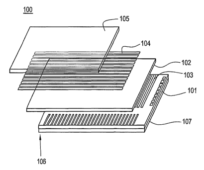
Fig. 1 shows an OLED structure 100 in accordance with an example embodiment
shown in a partially exploded view. The OLED structure 100 includes a
substrate 10 1
that is beneficially transparent to visible light. Illustratively, the
material chosen for the
substrate provides the desired strength and scratch resistance at the viewing
surface 106.
The substrate 101 is illustratively a polymer material, such as plastic, or a
suitable glass
layer, or a combination of glass, polymers and other materials. In example
embodiments
in which the substrate 201 is a polymer, the polymer may be polycarbonate,
polyolefin,
polyether sulfone (PES), polyethylene terephthalate (PET), polyethylene
naphthalate
(PEN), polyimide, and others. In an example embodiment such polymer layers
have a
thickness on the order of approximately 50 ~m to approximately lOs~m.
Additionally,
the substrate may include a nanocomposite film, which provides a barrier to
water vapor
and oxygen that is disposed over a suitable material that provides
flexibility.
Furthermore, layers of these materials may be used in various and sundry
combinations.
Regardless of its composition, substrate 101 beneficially is flexible so the
OLED
structure can be flexible.
Beneficially, the substrate 101 provides a base upon which the OLED devices
may be disposed, and is flexible. The substrate itself may also be barrier to
contaminants
such as water vapor, or oxygen, or both, and prevents contaminants from
reaching a
layer 102 that includes the OLEDs. Alternatively, another layers) to prevent
CA 02543425 2006-04-19
WO 2005/045948 PCT/US2004/035814
contamination maybe disposed over the substrate 101. In the example embodiment
of
Fig.l, an antireflection (AR) layer 107 acts as a barrier layer to
contaminants. As will
become clearer as the present description continues, a layer 105 is disposed
over layer
102 and protects layer 102 from contaminants. Quantitatively, it is useful for
the barrier
layers to provide a barrier to water vapor so that its permeation through the
barrier is
less than approximately 10 6 g/M2 /day and a barrier to oxygen so that the
permeation of
oxygen through the barrier is less than approximately 10-5 GM3/M2 /day.
Layer 102 is illustratively a multilayer structure that includes the OLEDs of
the
example embodiment. Illustratively, layer 102 is a three-layer stack comprised
of an
electron transport layer (ETL)/a light emission layer (EL)/a hole transport
layer. These
layers, which are not shown in Fig.2, are deposited by thermal evaporation or
spin
coating, and form the OLED layer of the OLED structure 100. Layer 102 may be
of the
type described in "Prospects and applications for organic light-emitting
devices" to
Burrows, et al. Current Opinion ih Solid State and Materials Science 1997. The
disclosure of this article is specifically incorporated herein by reference.
Anode lines
103 and cathode lines 104 are disposed on either side of the layer 102 to
provide the
necessary voltage to the OLEDs to effect illumination. These lines are
generally metal,
and are deposited by standard technique.
The cathode lines 104 are illustratively comprised of a low work function
metal
for electron inj ection. For example, the cathode lines may be Ca, Li, Mg or
an alloy such
as Mg/Ag, Al/Li or a multilayer material such as LiF/Al, Li20/Al, CaF/Al
structures. The
anode lines 103 must be substantially transparent to visible light. Indium tin
oxide (ITO)
with a surface modified to provide a high work function is used in this
capacity in the
example embodiment. To this end, ITO is a transparent conductive layer, which
is
coated on the substrate 101. ITO also injects holes to the EL layer via the
HTL. This
surface treatment can increase the worlc function, which results in a lower
potential
barrier to hole injection.
CA 02543425 2006-04-19
WO 2005/045948 PCT/US2004/035814
As can be readily appreciated, packaging is an important to the longevity of
OLED-based devices, which is particularly the case for OLED-based devices on
flexible
substrates. In the exemplary embodiments described herein, layer 1 OS is
comprised of a
plurality of thin metal layers and transparent dielectric layers that are
disposed in an
alternating or layered structure. The metal layers each have a thickness in
the range of
approximately 1 nm to approximately 1 OOrnn, and the transparent dielectric
layers each
have a thickness of approximately l Ornn to approximately 300nm. In order to
suitably
create a blaclc background by curbing reflections of environmental light and
to provide a
suitable contaminant barrier layer, one to ten stacks may be used to form
layer 105,
where as staclc is one layer of dielectric and one layer of absorbing metal.
Beneficially, the stress type of thin metal layers of the stacks of exemplary
embodiments is modified to be either tensile or compressive to compensate
stress of
dielectric layers (usually compressive) of the stacks. Therefore, compressive
stressed
film/tensile stress film will cancel the stress and the display will
not'curl.' Moreover, the
thin metal films are ductile and the dielectric layers, which are acting as
moisture barrier
layers, are divided into several thin layers separated by thin metal layers.
Advantageously, this structure is flexible and the moisture barrier layers
will not break
due to bending.
Another useful aspect of the structure of the layer 105 is its anti-reflection
property and its function as the back layer for a display device in which the
OLED
structure 10 1 functions. To wit, the laminated structure can only be put at
the back side
of the display, as the barrier/AR layer at the viewing surface must be
transparent to
visible light. As described in further detail herein, the layer 105 may be a
stack including
a quarter-wavelength dielectric layer, a reflective layer and a light
absorbing layer.
Finally, it is noted that a layer of hydrophobic material (not shown in Fig.
1, such
as a suitable hydrophobic polymer, may be disposed over rear-most surface of
the layer
105, and a backside substrate (not shown) is disposed over the layer 105 or
over the
hydrophobic layer. It is noted that unlike substrate 101, the back substrate
need not be
transparent, and thus may be chosen for its flexibility and its ability to
prevent
contamination, without regard to its transparency to visible light. Such
material include
but are not limited to polymers, metals, glass and other materials within the
knowledge
CA 02543425 2006-04-19
WO 2005/045948 PCT/US2004/035814
of one of ordinary skill in the art.
On the side of the substrate closest to the viewing side 106 an AR layer 107
is
disposed. The AR layer 107 beneficially prohibits the reflection of light
incident on the
viewing surface 106 (e.g., ambient light that impedes the viewing of the
output of a
display that includes the OLED structure 100 by the wash-out effect). To wit,
light
incident on the viewing surface from direction having components oriented
opposite to
the emission direction 108 of the OLEDs, is substantially prevented from being
reflected
at the viewing surface 106. As described in further detail herein, the AR
layer 107 may
be a multilayer dielectric stack that provides a cancellation effect of the
light incident on
the viewing surface. This physical phenomenon is well-known, and requires the
careful
selection of the thicknesses, indices of refraction and number of layers of
the dielectric
stack.
In addition to its antireflective properties, the dielectric layers of the AR
layer
107 provide a suitable barrier to prevent contaminants such as water vapor and
oxygen
from traversing the substrate 101 and reaching the layer 102 or other layers.
As such,
hermeticity at the viewing side 106 of the OLED structure is provided by the
dielectric
AR layer 107.
In example embodiments referenced above and described in detail herein, the AR
layer 107 serves as an antireflection layer to ambient light incident on the
viewing
surface 106. This AR layer 107 also provides flexibility, a barrier against
oxygen and
water vapor, and resistance to scratching. Layer 1 O5, which is on the side of
layer 102
opposite the viewing surface 106, provides the barrier against contaminants,
most
notably water vapor and oxygen. Layer 105 also provides a black or dark
background
for the viewing side 106 by reducing reflection of ambient or environmental
light. As
will become clearer as the present description continues, layer 105 may
include a
light-absorbing layer, such as an antireflecting dielectric stack to provide
this desired
daxk-background at the rear surface of the OLED structure 100. As can be
appreciated, a
black background is very important for a display to function in a bright
ambient or
baclcground lighting. Glares and surface reflection may prevent you from
viewing an
image if viewing the display in bright baclcground lighting such as sunlight.
In the
example embodiments, the dark or black background provides a sharp image with
CA 02543425 2006-04-19
WO 2005/045948 PCT/US2004/035814
comparatively reduced glare.
Fig. 2a shows a coating structure 200 for a rear layer 105 of the OLED
structure
100 in accordance with an example embodiment. The coating structure 200 is a
mufti-layer structure 201 disposed on the 'back' side of the OLED device
(e.g., on the
side of layer 102 that is opposite to the side closest to the viewing surface
106.) This
multilayer structure 201 includes at least one stack comprised of a light
absorbing layer
202, and a transparent layer 203. The light absorbing layer is illustratively
a metal, and
the transparent layer 202 is a dielectric material. In the example embodiment
there may
be one stack and as many as ten stacks. It is further noted that a layer of
dielectric 204
must be disposed between the first layer of metal in the multilayer structure
201 and the
cathode lines of the OLED structure. Finally, a hydrophobic layer 205 may be
disposed
between the mufti-layer structure and a rear or backside substrate 206. The
hydrophobic
layer 205 has a thickness in the range of approximately 10 nrn to
approximately 300 pm.
It is noted that oxygen is less damaging to the OLED devices than water vapor.
However, an oxygen barrier is much more difficult to realize. Material
structures with a
short atomic separation/distance and a lower propensity for the migration of
oxygen
atoms are particularly useful in this capacity. Dense, pinhole free, amorphous
structures
(without crystallization) may be used. It is noted that metal films may
readily crystallize
and a dielectric layer may form in a column structure; but with thin, and low
temperature deposition (such as magnetron sputtering on cooled substrates),
crystallization and column structures can be avoided. Such an oxygen barrier
layer may
be disposed between the rear substrate and the OLED device layer; for example
between
the hydrophobic layer 205 and the multilayer structure 201.
Illustratively, the absorbing layers 202 are dark metal layers as referenced
in
connection with layer 105 of the example embodiment of Fig. 1. These layers
foster the
dark background desired and allow for an improved contrast at the view
surface.
Moreover, these layers reduce the stress on the substrates. As described
previously, light
from the environment (sun light, lamps, etc) is competing with light emitted
from the EL
layer of an OLED. This 'environmental' light, which goes through the OLED
structure,
must be prevented from being reflected back to the observer's eye. The
multilayer
structure 201 performs this function, enabling the OLED structure to have
excellent
CA 02543425 2006-04-19
WO 2005/045948 PCT/US2004/035814
viewing contrast.
Absorbing layers 202 are usefully chosen to absorb visible light. Suitable
materials for the absorbing layers 204 include, but are not limited, to: thin
metal
coatings such as Mo, Zr, Ti, Y, Ta, Ni, and W; thin absorbing dielectric
materials such
as diamond-lilce carbon, SiOx, oxygen-deficient 1n203, ITO, Sn02, and similar
materials;
or semiconductor materials such as Si, Se, Ge, GaAs, GaN, Se, GaSe, Gale,
CdTe, TiC,
TiN, ZnS, ZnO, CdSe, InP and BN. Finally, it is noted that these layers are
deposited by
standard deposition techniques to a thickness in the range of 1.0 qm to
approximately
100 Vim, depending on the chosen material(s).
The transparent layers 203 are usefully dielectric layers with thicknesses of
approximately 20nm to approximately 300 nm. Suitable materials include, but
are not
limited to A1203, AION, BaF2, BaTi03, BeO, MgO, Gd03, Nb205, Th02, Ce02, Hf02,
Se203, SiO2, Si3N4, Ti02, Y3AI15012, ZeSi04, Ta205, HfN, ZrN, SiC, ByZSiO2o~
Depending on the material and wavelength these layers have a thickness in the
range of
100 ~.m to approximately 300 Vim. .
Finally, it is noted that by controlling the deposition process of the
materials of
the multilayer stack 201, the example embodiments afford a reduced substrate
curving
due to the stress of the film stack. To wit, by controlling the process, such
as through
sputtering pressure control, deposition rate and choice of material, the
stress induced can
be substantially nullity. For example, as described previously, the metal of
multilayer
structure (i.e., the light absorbing layers 202) can be chosen to have a
stress that negates
the stress of the dielectric layers 203. In another example embodiment, this
warping of
the polymer substrate may be prevented by coating each side of the polymer
with a
suitable inorganic material (e.g., glass) in order to nullify the stress.
An alternative structure to the coating structure 200 of Fig. 2a is shown in
Fig. 2b.
The multilayer stack 208 comprises a dielectric layer having a thickness equal
to a
one-quarter wavelength at a chosen wavelength that is desirably absorbed/not
reflected
back toward the viewing surface. The stack also includes a reflective surface
210, which
reflects the ambient light and a dark metal such as layer 203 above. In
addition to
absorbing light, the staclc 208 functions as an oxygen and humidity barrier.
To this end,
the materials chosen for the multilayer stack for optical extinction also
provide a barrier
CA 02543425 2006-04-19
WO 2005/045948 PCT/US2004/035814
layer to prevent water vapor and oxygen from reaching the OLED structure.
In the example embodiment the stack 208 forms the 'dark' background of the
OLED structure in a display. The multilayer stack 208 includes an optical
interference
structure that cancels light from direction 207 with the light reflected in
the direction
212 from different interfaces of the multilayer structure. This reflected
light has equal
intensity and opposite phase by virtue of the structure if the stack 208. Such
optical
interference structures are well known in the physical optical arts and are
often referred
to as dielectric stack filters. For example, the multilayer stack 208 may be
of the type
described in U.S. Patent 5,521,759, to Dobrowolski, et al., the disclosure of
which is
specifically incorporated herein by reference.
The dark metal layer 211 is disposed at the far side of the multilayer stack
as
shown. The layer 210 has a thickness in the range of approximately 50 ~m to
approximately 200 Vim, and also usefully suppresses reflections of ambient
light back
toward the viewing surface of the OLED structure. It is noted that if the
embodiment of
Fig. 2b is used, the dielectric layer 209 is usefully one-quarter wavelength
thick at
approximately 560 nrn (most sensitive wavelength region for human vision).
This layer
also provides a moisture barrier as well. Layer 210 is a metal that is
usefully very light-
absorbing, such as tungsten or inconel. Alternatively, oxygen deficient
InSnOx, or ITO
may be used as the light absorbing layer 210. It is noted that stoichiometric
ITO is a
transparent semiconductor, although its transparency decreases greatly and
conductivity
increases significantly if oxygen vacancies are increased in the material.
The layers described in connection with Figs. 2a and 2b may be formed at
temperatures below 100 'C by known electron-beam, sputtering or web coating
techniques, or a combination thereof.
Fig. 3 shows a coating structure 300 that is usefully disposed on the front,
or
viewing surface of an OLED structure (e.g., viewing surface 106 of the OLED
structure
100) in accordance with an example embodiment. For example, the coating
structure
may be used for the AR layer 107 of the example embodiment of Fig. 1. For
example
coating structure 300 may be used as the AR coating 107.
The coating structure 300 is a transparent structure that includes multilayer
structure 306 comprised of a barrier layer 301 disposed over a transparent
layer 302,
CA 02543425 2006-04-19
WO 2005/045948 PCT/US2004/035814
11
which is disposed over another transparent layer 303. The transparent layers
302, 303
are of the same materials and thiclcnesses as the transparent layers of Fig.
2. Transparent
layer 303 is disposed over or directly onto a substrate 304. The coating
structure 300 has
alternating relatively high index of refraction and relatively low index of
refraction
layers. This structure is commonly known as a'low-high-low' or an LHL stack,
and is
exceedingly useful in preventing reflections. It is noted that in keeping with
the LHL
stack structure, the coating structure may have more layers than the three
layers
specifically shown in Fig. 3.
The substrate 304 is usefully a polymer layer of a material such as described
above. The coating structure 300 disposed on the viewing side (e.g., 106) of
an OLED
structure beneficially reduces reflections from the viewing surface and
prevents
moisture from penetrating the substrate 304 and reaching the OLED region
(e.g., layer
102 of Fig. 1). However, all layers of coating structure are necessarily
transparent. Good
barrier layers are often materials having a high index of refraction. For
example,
excellent barrier layers such as A12O3 (n=1.65), Ti02 (n=2.2-2.3), Ta205
(n=2.1 to 2.2)
have a relatively high indices of refraction may be used according to an
example
embodiment. As such, it is noted that barrier layer 301 may be a polymer
material
chosen for its hydrophobic characteristics may be on top of dielectric layer.
With nL/nH/nL antireflection structure of an example embodiment, surface
reflection can be cut to less than approximately 2% or even approximately
0.5%. ITO is
a high index material, but by changing reactive sputtering gas or evaporation
gas during
the deposition, index matching of a polymer/plastic substrate with an OLED
structure
can be achieved to allow improved reflection from at the viewing surface.
It is noted that the additional transparent layers 303 may be disposed over
the
substrate 304. To this end, the transparent layers 303, and the barrier layer
301 comprise
a three-layer antireflection layer, provided the index of refraction of the
barrier layer is
less than 1.45. Moreover, the transparent layers 302, 303 having different
indices of
refraction are generally required for an inorganic material multilayer
antireflective
coating.
In accordance with an example embodiment, a multilayer antireflective coating
(e.g., multilayer AR coating 306) is used to enable a broad AR band and
provide a
CA 02543425 2006-04-19
WO 2005/045948 PCT/US2004/035814
12
relatively improved barrier to contaminants. The choice of each layer depends
on the
refractive index required, and the thickness required. For a three layer
coating, a known
condition for the electric vectors to be of equal magnitude and opposite sign
is:
Yi /Yo= Ya/ Y~= Y3/ Y2-~~~ Ys°b/Y3 (eqn. 1)
where yj (i=0, 1,2,3 .... ) is the optical admittance of the ith layer, ysub
iS the
optical admittance of the substrate and yo is the optical admittance of the
surrounding
medium. As such, if ns"bstra~e 1.52, a four-layer AR layer of an illustrative
embodiment
is: MgF (n=1.27 and a thiclcness of 92.7 nm)/Zr02 (n=2.06 and a thickness of
131.7
nm)/MgF (thickness of 30.3 nm)/ Zr02 (thickness of l6.Snm).
Finally, an index matching layer 305 of a material such as described in
connection with the embodiment of Fig. 2 is disposed over the substrate 304 as
shown.
This layer, like layers 301, 302 and 303 axe fabricated by known methods such
as those
described in connection with the embodiments of Fig. 2.
One of the layers of the antireflection layer comprised of the barrier layer
301,
and the transparent layers 302,303 beneficially is equal to the square-root of
the index of
refraction of the substrate 301. For example, ITO has a refractive index of
approximately 2.0 at 550 nm. The index matching layer 305 should have an index
of
refraction of approximately 1.81, making for example, Si 3N~, SiON, and BiO2
likely
candidates as the index matching layer 305. To wit, it is useful to provide an
index
matching layer, because any sudden change in index of two adjacent layers will
cause
reflection. Reflection will cause glare of the display, which is deleterious
for reasons
described above.
Finally, it is noted that nanocomposite clays can also be used as the barrier
layer
301 in this embodiment to prevent contaminants from reaching the OLEDs and to
prevent scratching.
Fig. 4 shows the Reflectance (%) versus wavelength (nm) for a three-layer AR
coating on a polymer substrate. The three layers are glass/W (7nm)/Al (80 nm).
As can
be appreciated the reflectance is beneficially insignificant over a useful
wavelength
range.
Fig. 5 shows the Reflectance versus wavelength for a six layer AR coating of
CA 02543425 2006-04-19
WO 2005/045948 PCT/US2004/035814
13
Glass/ W (6.lnm)/Si02 (78.5 nm)/W (15.3 nM)/Si02 (78.Snm)/A1 (71 nm). As can
be
appreciated, the greater the number of layers in the stack the better moisture
barrier
property. However, the reduction of reflections from the back side is mostly
curbed by
the first two or three absorbing metal layers.
The example embodiments having been described in detail in connection through
a discussion of exemplary embodiments, it is clear that modifications of the
invention
will be apparent to one having ordinary skill in the art having had the
benefit of the
present disclosure. Such modifications and variations are included in the
scope of the
appended claims.