Note: Descriptions are shown in the official language in which they were submitted.
CA 02544420 2006-05-O1
WO 2005/046095 PCT/FI2003/000848
1
ALL-OPTICAL SIGNAL PROCESSING METHOD AND DEVICE
FIELD OF INVENTION
The present invention relates to a method in optical signal processing and to
an optical
device for carrying out said method. More particularly, the invention relates
to all-
optical filters based on an optical resonator arrangement, which has a
capacity to store
temporally the electromagnetic energy of the incoming light and therefore has
some
memory about its past so that the filter can stay on a desired state for some
time
regardless of fast perturbations on the optical input signal. Such a filter
may be referred
to as a "slow" all-optical filter. The invention can be utilized, for example,
for optical
signal analysis, optical clock recovery, or for producing high-frequency
outputs from
lower frequency input signals, like e.g. optical microwave generation.
DEFE~TITIONS
The frequency of light is typically understood as the inverse of the
wavelength of the
electromagnetic field, i.e. v = e~(n~.) , where v is the frequency, c is the
speed of light in
vacuum, n is the index of refraction of the medium and ~. is the wavelength.
In the
context of this application, the word frequency, however, addresses to the
rate of
temporal, periodic intensity change of the light (e.g. a pulse frequency), and
is therefore
not connected to the wavelength. To highlight this conceptual difference, this
rate of
intensity change is called hereafter simply the frequency f, and the frequency
v as the
fundamental physical property of the electromagnetic field is discussed in
terms of
wavelength ~. . In other words, frequency f relates hereafter to temporal
pulses of light,
which pulses are formed from light having wavelength ~, , and frequency v
corresponding to said wavelength.
Due to historical reasons optical resonators are called sometimes as optical
cavities.
These two expressions are used interchangeably throughout the document.
CONFIRMATION COPY
CA 02544420 2006-05-O1
WO 2005/046095 PCT/FI2003/000848
2
BACKGROUND OF THE INVENTION
ELECTRICAL SIGNAL PROCESSING
Bandpass filtering is traditionally made with electrical means and optical
signals
processed by conventional methods require therefore optical-to-electrical
conversion
before the filtering can be performed. If the signal is transmitted further by
optical
means, one has to convert the filtered signal back to optical domain.
Conversion to and
from electrical domain is non-trivial with current state-of the-art whenever
signal
frequencies go above 40 GHz. The conversions forth and back generate also
additional
cost and possibly degrade optical signal quality. For example patent US
4,737,970
discloses a clock recovery device utilizing a cavity resonator in electrical
domain. The
present invention aims to all-optical conversion requiring thus no conversions
to and
from electrical domain and eliminating therefore any problems related to said
conversions.
ALL-OPTICAL SIGNAL PROCESSING
All-optical signal processing traditionally deals with different wavelengths
of light,
where e.g. different channels in WDM (Wavelength Division Multiplexing) system
are
separated from each other using optical filters having different wavelength
bands.
Optical processing based on temporal input signal frequencies, not wavelengths
of light,
has been done far less, but is also known from prior-art. Ring-resonators have
been used
for construction of all-pass optical filters (Azana and Chen, IEEE Photonic
Technology
Letters, 14, 2002) and together with Mach-Zehnder interferometers they
typically are
considered as basic building blocks of all-optical filters. Cascaded ring-
resonators and
Mach-Zehnder interferometers can be used to perform a Fourier-transform and
other
optical functions. Optical resonators have been used for all-optical signal
processing
(Lenz et al, IEEE J. Quantum Electron., 34, Aug. 1998) and clock recovery
(Jinno and
Matsumoto, IEEE J. Quantum Electron., 4, Apr. 1992). The clock recovery made
by
Jinno was based on simple optical resonator, whose optical length was
carefully matched
CA 02544420 2006-05-O1
WO 2005/046095 PCT/FI2003/000848
3
with: 1) wavelength of the incoming light and 2) data frequency. The device
is, however,
very limited in its capabilities to process more than one wavelength (or WDM
channel)
at time.
Some other all-optical filtering techniques are presented in the following
patent
publications. US 5,446,573 discloses an all-optical regenerator that is based
on the use
of a non-linear ring resonator. US 6,028,687 discloses a laser arrangement
between two
resonator mirrors for recovering a clock from a modulated optical input
signal. Here, bi-
directional mux/demux components , have been arranged within the resonator. US
6,388,753 discloses an all-optical bit phase sensor utilizing non-linear
interferometers,
where the refractive index of the non-linear material is varied.
SUMMARY OF THE INVENTION
Basically and generally expressed, the present invention relies on a method,
where the
processing of an optical input signal includes at least the steps of : 1)
excitating with at
least part of said input signal an optical resonator arrangement that
comprises two
substantially parallel, independent, complex one-pole resonators arranged in a
manner
that that one of said resonators is matched with the input signal and the
other one is non-
matched with the input signal, and 2) based on polarization separating further
from the
output of said optical resonator arrangement at least one optical output
signal so that
both said matched and non-matched resonators of said optical resonator
arrangement
contribute to the formation of said linearly polarized output signal.
The method may be carried out in practise, for example, by using a single
optically
birefringent resonator, whose output is further directed to a suitably located
polarization
selective device, that selects at least one direction of polarization from the
output said
birefringent resonator. In such an embodiment, the matched and non-matched
resonators
become formed inside said resonator arrangement due to the birefringency as
two
virtually independent resonators.
CA 02544420 2006-05-O1
WO 2005/046095 PCT/FI2003/000848
4
As will be shown later, the matched and non-matched resonators together with
the
polarization separating or selective device or means may be realized in
several ways and
using various types of optical elements. All the optical devices carrying out
the method
generate different types of bandpass filtering of the incoming optical signal
and provide
thus useful tools for various all-optical signal-processing applications.
The significant benefits of the invention include, for example, the fact that
the present
invention can be used to realize optical devices that process multiple
wavelength
channels simultaneously, that is to say in parallel. The invention requires
that the optical
length of one polarization mode of the resonator arrangement is matched with
the
wavelength of the incoming light, but it has no temporal signal length
requirements, i.e.
requirements for the duration regarding the rate of the incoming optical data.
The data
rate is matched by selecting, for example, suitable amount of birefringence
into the
resonator. The method of the invention thus enables parallel processing of
multiple
wavelengths simultaneously, provided that the resonator length is matched to
all used
wavelengths and the birefringence is suitable for the data rate.
One promising application of the invention can be found in all-optical clock
recovery.
However, the parallelism mentioned above holds true for all applications,
provided that
different wavelengths can later be separated from each other.
The most profound benefits of the invention vary according to the specific
applications.
When used for all-optical clock recovery the method liberates from the
dependency
between the resonator length (WDM channel separation) and the data rate. This
freedom
opens opportunity to build truly parallel systems in practise. When compared
to US
5,446,573, US 6,028,687, or US 6,338,753, the present invention requires
smaller
number of optical elements and gives thus simplicity of construction and
savings in cost.
In particular, the present invention does not necessarily require the use of
any optically
active medium (semiconductor optical amplifier or laser source) to provide
adequate
signal levels and operation. Tn its simplest form, the present invention
requires only the
CA 02544420 2006-05-O1
WO 2005/046095 PCT/FI2003/000848
use of one birefringent resonator arrangement together with one polarization
selective
element. For example, US 5,446,573 requires a non-linear ring, which consists
of two
laser sources, and four phase-modulators. US 6,028,687 requires an optical
mux/demux
element and at least two semiconductor optical amplifiers within an optical
resonator.
5 US 6,338,753 requires non-linear interferometer, whose refractive index is
varied with
external optical pulses, which in practice means a sufficient high-energy
laser build into
a working system.More details of the present invention are set forth in the
foregoing
description and in the accompanying drawings describing selected embodiments
of the
invention. The preferred embodiments and possible variants of the invention
will
become more apparent to a person skilled in the art also through the appended
claims.
It should be understood that in the following the purpose of the theoretical
and
mathematical descriptions is merely to function as tools for describing the
invention
better for a person skilled in the art. Therefore, even though the theory
might not be
completely immaculate in all respects, it nevertheless represents the
Applicant's best
understanding of the phenomena underlying the invention.
BRIEF DESCRIPTION OF THE DRAWINGS
In the accompanying drawings
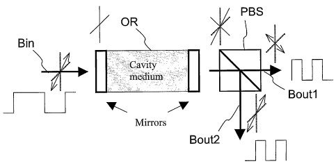
Fig. 1 A basic setup of an optical signal frequency filter according to the
invention.
Fig. 2 Phasor representation of the intracavity electric field.
Fig. 3 Step-pulse response of the intracavity electric field when r = 0.99 and
phase
is matched, i.e. ~p = 0° . The electric field has no imaginary
component.
Fig. 4 Step-pulse response of the intracavity electric field when r~ = 0.99
and phase
mismatch tp =10° . Due to the phase mismatch the field is complex. The
real
CA 02544420 2006-05-O1
WO 2005/046095 PCT/FI2003/000848
6
and imaginary parts of the electric field oscillate sinusoidally and have
phase-shift ~t~2.
Fig. 5 Transfer functions for ~p = 0.1 and ~p = 0 at r = 0.999 .
Fig. 6 Train of pulses (upper part) with period T =188.5 . Frequency
decomposition of the signal (lower part) reveals that it has energy peak at
angular frequency 0.1 rad h 1. Dashed line represents the Fourier-
transformation of rectangular signal, circles show the accurate energy
density position and magnitude of the periodic signal and peaks show the
computational FFT solution of the signal.
Fig. 7 Resonator response for square pulse excitation at angular frequency
~p~3.
Real and imaginary parts of the electric field (upper part) show strong
dependence on third harmonic component of the input excitation. The
intensity of the electric field (lower part), is flattened and does not
reflect
filtering property of the resonator. For comparison one period of the input
excitation (dashed line) is shown.
Fig. 8 Resonator has two axis of birefringence, symbolized with axis x and y.
The
polarization of incoming electric field has angle c~ with respect to the axis
of
birefringence and the polarization beam splitter divides the out-coming
electric field according to angle 9.
Fig. 9 System response with a resonator, where x-axis is matched ( ~p = 0 ), y-
axis is
non-phase-matched ( cp = 0.1 ), reflectivity is r = 0.999 , angle of input
polarization is c~ = 45° and angle of polarization beam splitter PBS is
8 = 45° . In the upper part the intensity components la , Iy , and Ib
are
CA 02544420 2006-05-O1
WO 2005/046095 PCT/FI2003/000848
7
depicted against a single period of excitation E;,~ . On lower part the final
output arms show an oscillating signal, which happens to be third harmonic
of the input pulse frequency.
Fig. 10 Properties of a train of Gaussian pulses with period T =125.7 to be
used as
input for a resonator.
Fig. 11 System response to the pulses defined in Fig. 10.
Fig. 12. Properties of a train of Gaussian pulses with period T =100 to be
used as
input for a resonator.
Fig. 13 System response to the pulses defined in Fig. 12.
Fig. 14 Burst of random data to be used as input for a resonator.
Fig. 15 System response to the pulses defined in Fig. 14.
Fig. 16 An embodiment of the device according to the invention using
polarization
controllers before and after resonator arrangement.
Fig. 17 A system with parameter values: r = 0.99 and 8 =75° , is
subject to change
of birefringence. This system is excited with a step-function. The system
intensity output Bout1 from arm 1 is depicted at three different phase-shift
values, namely ~po = 0 , ~p, =10° , and ~p2 = 20° .
Fig. 1~ A miniaturized embodiment of the device according to the invention.
CA 02544420 2006-05-O1
WO 2005/046095 PCT/FI2003/000848
8
Fig. 19 An embodiment of the device according to the invention with a first
polarization beam splitter in the front of the setup following two separate
resonators whose outputs are further combined with another polarization
beam splitter.
Fig. 20 An embodiment of the device according to the invention based on the
use of
a micro sphere resonator.
Fig. 21 An embodiment of the device according to the invention based on the
use of
photonic bandgap structures.
DETAILED DESCRIPTION OF THE INVENTION
In the following the invention is mainly described referring to a birefringent
resonator
arrangement, where the matched and non-matched resonators are formed within a
single
physical cavity due to the birefringency. However, the invention is not
limited to such
embodiments, but the invention may also be realized using separate matched and
non-
matched resonators. One example of such an embodiment is later given in Fig.
19.
In the Figs 1,16,19 and 20 the polarization axes are depicted with "crossed"
markings
using both solid and dashed lines.
It is known from prior-art, as such, that an optical resonator behaves as an
one-pole
complex filter. Complex one-pole resonators generally, working either in
optical, digital-
electronic etc. domain, are able to transform purely real input signal to a
complex one.
Only when the wavelength of excitation is matched with the resonator, it has
lowpass
filtering function with no imaginary parts and therefore, it can directly be
used for signal
processing purposes. Alternatively, if the wavelength and rate of data both
are matched,
then it operates as a bandpass filter. However, when the wavelength of
excitation does
not match with the resonator, it always behaves as a complex bandpass filter.
Although
CA 02544420 2006-05-O1
WO 2005/046095 PCT/FI2003/000848
9
real and imaginary parts both pass only a narrow band of signal spectrum with
equal
gain, they differ Tc l 2 in phase. While the optical output is always measured
as the
square of amplitude (i.e. intensity) and because of the quadratic phase-shift
between real
and imaginary parts of the signal, the output is flattened out and the
resonator cannot be
used directly as a bandpass filter (later this will be shown graphically).
If one could separate real and imaginary parts from each other, or suppress
one of them,
the resonator bandpass characteristics could effectively be utilized also in
case of
wavelength mismatch. The current invention provides a novel and inventive way
of
doing this.
The key of the invention lies in the novel way of taking into use the
potential bandpass
filtering capabilities of an optical complex one-pole resonator by, 1)
excitating with at
least part of the input signal an optical resonator arrangement that comprises
two
substantially parallel, independent, complex one-pole resonators arranged in a
manner
that one of said resonators is matched with the input signal and the other one
is non-
matched with the input signal, and 2) based on polarization separating further
from the
output of said optical resonator arrangement at least one optical output
signal so that
both said matched and non-matched resonators of said optical resonator
arrangement
contribute to the formation of said output signal.
As will be shown later, such an arrangement, that may be realized for example
by using
a birefringent resonator combined with a polarization beam splitter, will be
able to
amplify the real part of the mismatched optical field and suppress the
imaginary part.
Therefore, the output of such resonator-polarizes setup can be made highly
dependent on
the filtering properties of the complex one-pole resonator.
Figure 1 describes schematically one embodiment of the invention combining a
birefringent optical resonator OR with a polarization beam splitter PBS in
order to
divide the light beam Bin inputted in said system into two separate optical
arms Boutl,
CA 02544420 2006-05-O1
WO 2005/046095 PCT/FI2003/000848
Bout2. This basic setup can be realized in a variety of different ways, as
will be shown
later.
In the following some basic principles of optical resonators are first
discussed. Real and
5 imaginary part transfer functions of a complex one-pole resonator are
presented and an
intensity output of the resonator is presented. Especially, the consequence of
the
birefringence of the resonator OR and the effect of the inclusion of a
polarization beam
splitter PBS at the resonator output are explained. Finally, selected examples
of systems
according to the invention, and using various optical excitation forms are
presented
10 together with some applications.
OPTICAL RESONATOR AND PHASORS
Amplitude and phase of an electric field inside an optical resonator can be
presented
with phasors as depicted in Fig. 2. At time t = 0 an electric field E,.,1 (0)
is injected into
the resonator. After one round-trip the electric field amplitude is decreased
by factor
r ~ ~0,1~ and has experienced a phase-shift cp (in following the phase-shift
~p is
understood to be a modulo of 2~ ). Additionally, a new field-component is
added giving
a total electric field E (1) = re'~E"1 ~0) + E"~ (1) . After fa number of
round-trips the
intracavity electric field becomes
n p
E(~e)=~(re~) E;,~~rz-p)=re'~E(n-1)+Ei,l(n), (1)
p=0
where n = t~trt is the round-trip number and t,~ is the duration of a single
round-trip.
Optical resonator, as a one-pole complex filter, will produce complex electric
field
inside the resonator in presence of phase mismatch ~p . Buildup of energy
under constant
injection in an arbitrary resonator ( r = 0.99 ) with phase mismatch cp =
0° and ~p =10°
are depicted in Figs 3 and 4, respectively.
CA 02544420 2006-05-O1
WO 2005/046095 PCT/FI2003/000848
11
When phase is matched ( ~p = 0 ), the energy starts to build up within the
resonator and
the net electric field has no imaginary part. Now the resonator behaves as a
low-pass
filter and has time constant 2 = .~~(-c In r) for light intensity, where c is
the speed of
light within the medium, ~ is the one-pass length of a Fabry-Perot resonator
and r- is
one-pass loss factor of light intensity within the resonator.
When phase is not matched, the electric field becomes complex and the phasor
draws a
converging spiral loop. As visible in Fig. 4, and as known from prior-art, the
real and the
imaginary part of a causal signal are connected through Hilbert-transform.
Impulse response of the resonator is
j2 ( 12) _ ( re's ~~~ a ( yi ) (2)
where a (zz) is the step-function (Heaviside function) due to causal nature of
the
response. Fourier-transform of the impulse response of real and imaginary
parts give
transfer functions
TR°~~~-2, i~-ln(re'~)+ico-ln(r-e'~) (3)
and
TL"~~~ 2 iw-ln(r-e'~) iw-ln(re'~) ~ (4)
where eo = 27c f = 2~'~~ is an angular frequency expressed in units of rad~n .
Transfer
functions for ~p = 0.1 and ~p = 0 at r- = 0.999 are illustrated in Fig. 5.
Bandpass filtering
property of the optical resonator at phase mismatch and lowpass property at
phase match
are evident. By increase of cavity finesse, i.e. r- ~ 1, the filter becomes
increasingly
selective.
CA 02544420 2006-05-O1
WO 2005/046095 PCT/FI2003/000848
12
Filtering property of the resonator is now shown in time domain for a periodic
input. Let
us assume a train of pulses with period T =188.5 as shown in Fig. 6. Frequency
decomposition of the signal reveals that it has the fundamental angular
frequency at
130 rad fa-' , its second harmonic is suppressed and it has third harmonic at
0.1 rad fi 1.
When such signal is fed into a resonator with phase mismatch ~p = 0.1 and r =
0.999 we
could expect that real and imaginary parts of the signal reflect this third
harmonic
component while all other frequency components are highly suppressed. This
becomes
evident from Fig. 7 upper part. Because the amplitudes are nearly the same and
phase is
quadratically shifted between the real and imaginary parts of the signal,
modulus of the
complex signal remains approximately constant. In phasor representation the
vector
would draw just a circle with nearly constant radius. Intensity output 1 ~ EE'
is thus
flattened as shown in the lower part of Fig. 7. It is evident that such
resonator is hardly
usable as a bandpass filter at wavelength mismatch. The situation would
change,
however, if either real or imaginary part of the signal could be suppressed.
OPTICAL RESONATOR BIREFRINGENCE AND POLARIZATION BEAM SPUTTER
When an optical resonator OR is birefringent, the path lengths inside the
resonator are
uneven for orthogonal polarization components. When this type of resonator is
combined with a polarization beam sputter PBS and circulating electric field
has phase-
matched and non-phase-matched components, the imaginary part of the electric
field
component can be suppressed. In other words, according to the present
invention the
system output can be made strongly dependent on the real part electric field
of the
mismatched resonator and such system behaves as an optical signal bandpass
filter.
Let's define x-axis of the resonator phase-matched and y-axis non-phase-
matched, the
amount of mismatch symbolized by cp . Intracavity electric fields are
Ex ~n~ = rEx ~n-1~+E,.",x ~h~ (5)
and
CA 02544420 2006-05-O1
WO 2005/046095 PCT/FI2003/000848
13
Ey (n) = re'~'Ey (n -1) + E;",y (f2) . (6)
We assume that the incoming field has angle c~ with respect to the axis of
birefringence
of the resonator OR and the polarization beam splitter PBS divides the
outcoming
electric field according to angle 8 , as shown in Fig. 8. The polarization
beam sputter
PBS outputs Boutl and Bout2 are labeled below in the equations shortly as
optical arms
1 and 2. This holds true especially for a polarization beam splitter, but it
should noted
that the invention is not limited to the use of a polarizarion beam splitter,
but any
suitable polarization separating or selecting means may be employed. It can be
shown
that the output intensity of the polarization beam splitter PBS is
cost B sinz 8 sin 29/ Ix
I, 2
IZ sin2 B cost 6 -sin 2~/ ~6 (7)
where Ix = ExEx , Iy = E~,EY , and I6 = ExEy + EzEy = 2Ex Re Ey . As present,
the
oscillating, or beating, term Ib is independent on imaginary electric field Im
E~, when
the field Ex is matched with the resonator.
In order to show the effect, the same pulse excitation than in previous case
is used with a
resonator, where x-axis is matched ( ~p = 0 ), y-axis is non-phase-matched (
~p = 0.1 ),
reflectivity is r = 0.999 , angle of input polarization is c~ = 45° and
angle of polarization
beam splitter PBS is B =45° . In the upper part of Fig. 9 the intensity
components Ix,
1?, , and Ib are depicted against a single period of excitation E,.,~ . The
oscillating term
clearly reflects the absence of imaginary component and the real component of
the
electric field is amplified by Ex . On lower part of the Fig. 9, the final
output arms show
an oscillating signal, which happens to be third harmonic of the input pulse
frequency.
The operation can be proved also for other type of signals. A train of
Gaussian pulses
with period T =125.7 , as depicted in Fig. 10, is fed into the same resonator
than used
CA 02544420 2006-05-O1
WO 2005/046095 PCT/FI2003/000848
14
previously. The second harmonic of the frequency decomposition is exactly at
resonance
frequency of the resonator and, therefore, we can expect this second harmonic
component to be passed by the filter. This is exactly what happens as depicted
by Fig.
11. If the same train of pulses period slightly changed ( T =100 ) and thus no
frequency
components at resonance frequency, is fed into the previously introduced
resonator, the
filter output is essentially flat. For this effect, see Figs 12 and 13, where
said effect
becomes obvious for any person skilled in the art.
APPLICATIONS, ALL-OPTICAL MULTIWAVELENGTH CLOCK RECOVERY
One interesting application of the invention can be found in all-optical clock
recovery.
When compared to prior art solutions to make all-optical clock recovery by use
of
Fabry-Perot resonator, the arrangement of the invention is superior by its
ability to
operate simultaneously at multiple wavelengths. A burst of data (half of bits
randomly
shut off) with clock period T = 62.8 is fed into the resonator OR as shown in
Fig. 14.
The output of the resonator OR is depicted in Fig. 15. For sake of clarity
only arm 1
(Boutl) is plotted. This case illustrates very well the properties of the
invented system. It
selectively filters the angular frequency, which is in match with the
resonance frequency
of the unmatched polarization component, and in addition to this, it maintains
the
operation for some time depending on resonator finesse. Optical resonator can
be
thought as an temporal energy store. Now it stores and maintains the
oscillation it has
picked up for a certain time.
In the following an example calculation of making filtering at several
wavelengths
simultaneously is given.
We shall assume a set DWDM channels (Ov = 100 GHz) operating at s~ = 1550 nm
wavelength region. Data rate at each channel is f = 40 GHz. A resonator medium
has
refractive index y2 = 1.5 . In following we will determine the required Fabry-
Perot
resonator length .~ , degree of birefringence W 2, and one-pass intensity loss
factor r for
simultaneous operation of the system at multiple wavelengths.
CA 02544420 2006-05-O1
WO 2005/046095 PCT/FI2003/000848
Resonator x-modes are set to coincide with channel separation of the DWDM
system,
i.e., Ov = c~(2h~) , which gives the resonator length .~ =1 mm . The DWDM
channels
would also be matched with resonator modes when the length is integer multiple
of .~ , as
5 clear for the persion skilled in the art.
The filtered frequency is dependent on the difference of x- and y-mode
refractive indices
f - C012 (g)
~h
which determines the required degree of birefringence to be 0n = 3.1 ~ 10-4 at
s1, _
10 1550.00 nm.
As present from Eq. 8 the filtered frequency is dependent on the wavelength of
light.
While different channels have slightly different wavelength, the filtered
frequency is
also changed. The difference in filtered signal frequency can be expressed in
function of
15 the wavelength change
d f - _ c~f2 d~. . (9)
~.ZTt
The channel separation can be expressed in terms of wavelength d~, _ -~,Zdv~c
= -0.8
nm, which translates to shift of filtering frequency according to following
Table 1.
Passband of a Fabry-Perot resonator is defined as
Sv = In f-I c ( 10)
2TC~z.~
The filter operates for those DWDM channels where the filtering frequency f
shifts stays
within the passband of the resonator. This happens when df < 0.5 w.
CA 02544420 2006-05-O1
WO 2005/046095 PCT/FI2003/000848
16
Channel d~. (nm)df (GHz)
#
0 0 0
1 -0.8 0.02
2 -1.6 0.04
-8.0 0.21
-16 0.41
50 -40 1.03
Table 1.
The passbands and the number of possible simultaneously processed channels fox
5 various loss factors r- are presented below in Table 2.
r 0.5 w Channel d~, df
(GHz) shift mar.(~) (GHz)
#
0.9 1.68 81 64.87 1.67
0.99 0.16 7 5.61 0.14
0.998 0.03 1 0.8 0.02
Table 2.
10 As can be seen, the resonator is capable of processing smaller number of
channels the
lower the loss factor (higher the mirror reflectivity) is. High loss factor
(low mirror
reflectivity) gives larger number of channels to be processed, but with lower
capability
for recovery (the energy storage of the resonator is lossy). One has to make a
tradeoff
between the number of processed channels and the capability to recover the
clock signal.
The situation can be compensated by suitable control of the wavelength
dependence of
the birefringence ~fa (~,) .
CA 02544420 2006-05-O1
WO 2005/046095 PCT/FI2003/000848
17
One possible setup contains, as depicted schematically in Fig. 16, a first
polarization
controller PC1, a Fabry-Perot type fiber optical resonator OR with ability for
a fiber
twist, second polarization controller PC2, and a polarization beam splitter
PBS.
The first polarization controller PCl sets the state-of polarization of
incoming light such
that the angle of polarization (azimuth) differs from the axis of
birefringence of the
resonator OR. Should they completely coincide, no oscillation may be observed
at the
output while all energy is directed either on matched or non-matched resonator
mode.
In this embodiment, the fiber optical resonator OR is constructed by coating
cleaved or
polished fiber end with high reflectivity dielectric coating. The fiber length
is chosen
such that free spectral range (FSR) is matched with the channel spacing of the
incoming
light. The optical length of the resonator is regulated in order to keep the x-
mode optical
length matched with channels of the incoming light. In the context of this
invention the
aforementioned matching is shortly referred to as mode-locking and in addition
to a fiber
resonator it applies also to other type of resonators. Instead, or in addition
to adjusting
the length of the resonator, mode-locking may also be achieved by tuning the
wavelength of the incoming light. The resonator has preferably low internal
loss and has
high reflectivity dielectric mirrors. The degree of birefringence, and thus
the angular
frequency of the mismatch, is adjusted by twisting the optical fiber
constituting the
resonator. The amount of angular frequency mismatch should be equal with the
angular
frequency of the incoming data.
Second polarization controller PC2 sets the state-of-polarization of the
resonator OR
output such that the polarization beam sputter PBS divides signals suitably
between the
two output arms B out l, B out2.
If the processed signal has multiple wavelengths (channels), each channel
should have
data frequency matched with the degree of angular mismatch from channel to
channel.
CA 02544420 2006-05-O1
WO 2005/046095 PCT/FI2003/000848
18
The phase may differ. Later one may want to separate channels from each other,
but this
speculation and related techniques are beyond the scope of the present
invention.
In the following certain variations and alternatives for the different parts
of the setup
carrying out the invention have been listed. These apply to the clock recovery
application already explained, but are also applicable, mutatis mutandis, to
other
applications and optical setups described in this text. Further, one should
not consider
the invention to be limited even by these variations and alternatives, but the
invention
should be restricted only in the manner indicated by the scope of the claims
appended
hereto.
The resonator OR does not need to be of a Fabry-Perot type, but it could also
be, for
example, a fiber loop resonator (preferably with weak input and output
couplings). It
may also be a micro-ring, -sphere, -toroid or a photonic bandgap resonator. In
such
"non-Fabry-Perot" loop or ring type resonators the optical medium is arranged
to form at
least partly closed optical circle where the light travels substantially only
one common
direction without multiple back-and-forward reflections.
The cavity medium of the resonator OR may constitute of a normal single mode
fiber or
polarization maintaining fiber. However, the setup may also be build
completely without
any fiber optic components. The required optical functions can be achieved
with free-
space optics or integrated optics. Therefore, the resonator OR could be, for
example, a
coated dielectric rod, a pair of free-space dielectric mirrors or even a
semiconductor
device. The cavity medium may be simply air or other transparent gas or liquid
instead
other optically transparent, dielectric or semiconductor materials. It should
be noted, that
the invention is not limited only to visible wavelengths, but it can be used
broadly with
any optical wavelengths that may be shorter or longer than visible
wavelengths. It is also
obvious for a person skilled in the art that certain coherence of the inputted
light is
required.
CA 02544420 2006-05-O1
WO 2005/046095 PCT/FI2003/000848
19
The "mirrors" of the resonator OR may be, for example, dielectric stack
mirrors, metallic
mirrors, fiber loop mirrors, fiber couplers (not really a mirror, but input
port with weak
efficiency) or different type of waveguide couplers. Further, said mirrors may
have
different reflectivities for x- and y-directions. High reflectivity mirrors
are typically
desired.
Light is necessarily not coupled into the resonator OR through the
aforementioned
mirrors, but evanescent coupling, or any other optical coupling methods known
in the art
may also be used. Input coupling may be realized, for example, with prisms
arranged in
planar waveguides.
The degree of birefringence in the resonator OR can be adjusted with not only
twist, but
also by stress, tension, bend, or other structural deformations of the cavity
medium.
Temperature and electro-optical effects may also be used to affect the
birefringence of
the resonator depending on the cavity medium/material. For example, if the
cavity
medium is gas or vacuum, then the birefringency of the resonator may be
altered by
deformation of the end mirrors or corresponding cavity forming reflectors.
As already mentioned, the resonator arrangement does not need to based on a
birefringent cavity, but instead it may also be formed from two physically
separate
resonators one matched with the incoming light and the other one non-matched
with the
incoming light. The polarization state of the incoming light is required to be
such that
both of these resonators participate in the formation of the final output
signal available
after the polarization separating means.
Polarization controllers PC1,PC2 before and after a resonator OR, as shown
schematically in Fig. 16, may not be necessary at all if the polarization of
the incoming
light is already suitable for the resonator OR, and the selection angle of the
polarization
beam sputter PBS is correct or it can be adjusted.
CA 02544420 2006-05-O1
WO 2005/046095 PCT/FI2003/000848
Polarization separating means may be a beam splitter PBS or any optical
component or
set of components known in the art, which selects or separates at least one
polarization
component from the inputted light. It is not even necessary to divide the
polarization
components of the light into different optical arms, but one of these
components may be
5 absorbed or otherwise dumped during the separation process. Possible devices
include,
but are not limited to the following : Wollaston prism, Glan-Foucault
polarizer, Nicol
prism, Rochon prism, dielectric coating polarizer, wire grid polarizer,
polymer based
film polarizer, single polarization mode transmitting fiber, photonic crystal
polarization
separator. The polarization separation means do not need to be comprised in a
separate
10 optical component, but itlthey can be, for example, integrated directly on
the output side
of the resonator arrangement.
In case when the birefringence of the resonator OR is wavelength dependent,
then the
extracted frequency may vary from inputted channel to channel, i.e. data rate
is xx GHz
15 for inputted channel one, yy GHz for channel two etc.
The mode locking may be active or passive. For example, if the light source is
in
vicinity of the resonator OR, the out-leaking light from resonator OR may be
used to
feed some light back to the coherent light source (typically laser). For the
correct
20 operation of the setup, however, the resonator OR is typically required to
be
substantially mode-locked with the incoming light / light source.
The excitation of the system according to the invention may be due to change
of the
incoming light intensity, change of its polarization, change of the resonator
length (so
that x-axis also becomes non-phase-matched), or change of the resonator medium
refraction index. The excitation may be generated by the light source, an
external
modulator (modulating light intensity or polarization), or coupling strength
of the input
port of the resonator. Also the input port coupling strength may be modulated.
Excitation
forms may be periodic: train of square pulses, Gaussian pulses, solitons
(sech), or non-
periodic: stream of data . Other type of input signals may also be used.
Therefore, the
CA 02544420 2006-05-O1
WO 2005/046095 PCT/FI2003/000848
21
excitation may be due to the properties of the incoming light itself, or the
excitation may
also be accomplished by altering the properties of the resonator arrangement.
APPLICATIONS, SIGNAL FREQUENCY COMPONENT ANALYSIS
The setup described schematically in Fig. 16 can be used for input signal RF-
component
analysis when equipped with at least one optical sensor (photodiode) and means
to read
the sensor output. Preferably, photodiodes or other type of fast optical
sensors are
arranged to sense the output of at least one optical signal Bout1 and/or
Bout2. The
degree of birefringence of the resonator OR is swept (by e.g. twist) such that
the optical
frequency phase mismatch goes step-by-step from 0 to ~z While each optical
frequency
mismatch corresponds to a certain radio frequency of the signal, the output
signal
Boutl,Bout2 amplitudes are read during the sweep. One can thus obtain
information
about signal frequencies of the incoming signal Bin. In this configuration one
utilizes the
one-pole complex resonator frequency selectivity for inspection of optical
signal quality.
APPLICATIONS, HIGHER HARMONIC SIGNAL GENERATION
The setup of the previous cases explained abobe (Fig. 16) can be used for
optical
microwave generation when further equipped with suitable optical light source.
As
explained and illustrated in already earlier in this application, the higher
harmonics of,
e.g. train of square pulses, can be extracted if the input signal contains
higher harmonic
components, like some odd harmonic of a train of square pulses.
APPLICATIONS, MEAS UREMENT OF BIREFRINGENCE
The filtering property of a resonator system according to the invention is
dependent on
the degree of birefringence in the optical resonator OR . This property can be
used for
the measurement of minute birefringence in the following way.
When the system is excited with an optical signal Bin, which includes multiple
ranges of
frequencies, or continuum of frequencies, the change of filtering frequency
can be
determined from frequency output oscillations. An example of a signal with
continuum
CA 02544420 2006-05-O1
WO 2005/046095 PCT/FI2003/000848
22
of frequencies is a step-function, and a signal with multiple frequencies is,
for example,
a periodic sinc signal.
A system with parameter values: r- = 0.99 and B =75° , is subject to
the change of
birefringence. This system is excited with an inputted step-function. The
system
intensity output Boutl from arm 1 is depicted in Fig. 17 at three different
phase-shift
values, namely ~po = 0 , gyp, =10° , and ~pz = 20° . As present,
the oscillating frequencies
are dependent on the changes of the birefringence. The oscillation will dampen
out while
the excitation continues unchanged.
If we know the initial state of the studied optical system, i.e., its
birefringence, the
change of oscillation frequency is an indication of the change of
birefringence. While
the' oscillation will dampen out on course of time, the excitation should be
repeated at
some time interval.
An alternative way to measure birefringence is to excite the system with a
periodic
signal, whose fundamental frequency, or some of its harmonics, coinside with
the
filtering frequency of the resonator system. The excitation frequency is
actively tracking
the filter transmission maximum by, e.g., using a voltage controlled
oscillator. If the
filter output amplitude decreases, the excitation frequency is adjusted such
that the
output amplitude reaches again its maximum. Thus, the frequency of excitation
is an
indication of the birefringence of the optical system.
APPLIeATIONS, MINIATURIZED EMBODIMENT
The invention may also be realized as a miniaturized optical arrangement
described
schematically in Fig. 18. Optical resonator OR may be realized as a
miniaturized (just a
few mm in dimensions) Fabry-Perot etalon whose both optical ends have been
coated
with a dielectric reflective coatings. Polarization selective element PBS is a
miniature
size polarization beam splitter or polymer film polarizer. According to one
embodiment,
the PBS could be cemented or integrated directly right after the optical
resonator OR. In
CA 02544420 2006-05-O1
WO 2005/046095 PCT/FI2003/000848
23
Fig. 18 only one optical arm of the PBS is utilized, and the useful light is
amplified with
semiconductor optical amplifier SOA and then directed to output. The input and
output
could naturally comprise additional optical elements, like lenses for focusing
or
waveguides for light transmission. The optical resonator OR temperature is
regulated
with one or more thermoelectric coolers TEC1, which stabilize the optical
resonator OR
temperature to a desired value. This is needed to keep the resonator
transmission modes
stable and the optical resonator OR mode-locked with the wavelengths of the
incoming
light. The device package P may include still further thermoelectric coolers
or
temperature regulators, although they have not been depicted in Fig 18. The
birefringence of the optical resonator OR can in fact be controlled with,
e.g., two or
more thermoelectric coolers. When two or more temperature regulators are
connected to
the optical resonator OR, they can be used to create a temperature gradient,
which
induces birefringence on the optical resonator OR. By controlling the
temperature
difference and the average temperature, one may simultaneously adjust the
optical
resonator OR birefringence and the mode-locking property. Alternatively, a
pair of
electrodes, whose electric field induce and control the amount of
birefringence, can also
be used for birefringence control.
OTHER APPLICATIONS AND FURTHER VARIATIONS
The invention can be used for wide variety of applications related to all-
optical filtering.
Because of the auto-regression nature , i.e. "memory" of the filter, filtering
does not
however apply for very fast changes. For certain applications, this may be a
desired
feature instead of a limitation.
Again, it needs to be emphasized, that while the invention has been shown and
described
here with respect to a few selected embodiments, it should be understood that
these
embodiments are only examples, and that a person skilled in the art could
construct other
embodiments utilizing technical details other than those specifically
disclosed herein
while still remaining within the spirit and scope of the present invention. It
should
therefore be understood that various omissions and substitutions and changes
in the
CA 02544420 2006-05-O1
WO 2005/046095 PCT/FI2003/000848
24
optical design of the resonator arrangement, polarization selective element
and related
optical components coupling light in and out from said components, as well as
in the
mutual organisation and operation of the same, may be made by those skilled in
the art
without departing from the spirit of the invention.
For example, according to the invention it is also possible to arrange a first
polarization
beam sputter PBS1 in the beginning of the setup, then two resonators OR1 and
OR2
(one matched and other non-matched), whose outputs are further combined with
another
polarization beam splitter PBS2. This embodiment is schematically shown in
Fig. 19.
The polarization axes of beam splitters PBS 1 and PBS2 are depicted with solid
line. The
polarization axes of PBSl, which determines the principle polarization axis of
the whole
system, are illustrated with dashed lines in other parts of the system.
Components M1-
M3 are mirrors. Here, instead of a single birefringent resonator arrangement
the
resonator arrangement comprises two physically separate individual resonators
ORl and
OR2.
The setup according to the invention has been shown in the above examples to
operate in
transmission. However, it should be obvious for a person skilled in the art
that
embodiments also operating in reflection are possible. The resonator
arrangement OR
may thus be realized in such a way that the light inputted in the resonator
through a port
(typically a mirror) outputs from the same port. In the above given examples
the
resonator has been arranged with separate ports for input and output.
As a general way of optimizing the performance of the optical setup according
to the
invention, the angle of the linear polarization of the incoming light may be
adjusted
respect to the polarization axes of the resonator arrangement so that the
oscillations at
the output are maximized. Similarly, the angle of the polarization separating
element
after the resonator arrangement may be adjusted for the same purpose.
A light amplifying optical element or light amplifying means may be arranged
in front
of the resonator arrangement, after it or within it. Preferably, such an
element is arranged
CA 02544420 2006-05-O1
WO 2005/046095 PCT/FI2003/000848
between the resonator and the polarization separating means. Suitable light
amplifying
elements include, for example, active optical fibers and other active
waveguides, which
are typically based on the use of rare-earth element doped materials. Another
possibility
is the use of various semiconductor optical amplifier (SOA) devices as shown
in Fig. 18.
5 Figure 20 describes schematically still one possible embodiment of the
device according
to the invention based on the use of a micro sphere resonator. A waveguide is
arranged
to couple the incoming light Bin into the resonator OR, and another waveguide
couples
the light out from the resonator to a polarizing beam splitter PBS.
10 Fig. 21 depicts how the device according to the invention may be
manufactured using
photonic bandgap structures. Expressed in more general terms, the device may
be
manufactured by use of light scattering periodic microstructures. Such a
device can be
built in the size of minimum of few tens of micrometers. A solid-state
substrate medium
(like glass, silicon, or suitable polymer) can serve as the base for periodic
15 microstructures. The incoming light Bin can be guided along the missing row
of
microstructures. Optical resonator OR can be formed using two or more
microstructures,
or it may be formed in the shape of a ring, and the outcoupled light can be
guided to a
photonic crystal polarization beam splitter PBS. Fig. 21 is purely
illustrative and
microstructure form, size, pitch, aspect ratio, etc. are dependent on used
wavelength and
20 optical design.