Note: Descriptions are shown in the official language in which they were submitted.
CA 02544774 2006-04-24
LAMP POWER SUPPLY AND PROTECTION CIRCUIT
FIELD OF THE INVENTION
The present invention relates to a cold cathode fluorescent lamp (CCFL)
circuit, and more particularly to current control of a CCFL circuit.
BACKGROUND OF THE INVENTION
CCFL technology is being used more frequently for illumination in various
types of display systems due to improved durability and efficiency over
conventional
methods. For example, CCFL technology is used for backlighting of LCD monitors
or other computer displays. Additionally, CCFL technology is used in signs and
instrumentation. Typically, an AC line voltage provides power for operating a
CCFL
device. A power supply or ballast is used to convert the AC line voltage to a
voltage
suitable for the CCFL device.
Variations in certain parameters of a CCFL system may adversely affect the
operation of the power supply, the lamp, and/or other components. When the
power
supply provides power for more than one lamp, the performance of a first lamp
may
affect the performance of a second lamp. If the first lamp burns out or is
otherwise
damaged, the voltage and/or current of the second lamp may be affected. In
other
words, in typical CCFL systems, the impedance of each lamp affects the overall
performance of the CCFL system. Factors that determine the impedance of a lamp
include size (i.e. length), temperature, and other process variations.
2
CA 02544774 2006-04-24
Generally, a CCFL system provides a voltage based on particular lamp
requirements. For example, the power supply provides a voltage for a
particular
lamp size. If the CCFL system is operated with an improper lamp (i.e. a lamp
that is
too large or too small), damage may occur to the lamp or other component of
the
CCFL system. Therefore, different power supplies must be used for different
lamps.
Additionally, if the CCFL system is operated with a missing or damaged lamp,
damage may occur.
SUMMARY OF THE INVENTION
A power supply device for a lamp comprises a voltage regulating module that
receives an input voltage signal and generates an output voltage signal that
is
substantially constant. A voltage driving module receives the output voltage
signal
and a detection signal, and generates a driving voltage signal. A current
limiting
module receives the driving voltage signal and generates a current supply
signal that
is substantially constant regardless of an impedance of a load that receives
the
current supply signal. A detection module communicates with one of the current
limiting module, the current supply signal, and/or the load, and generates the
detection signal. The detection signal is indicative of a voltage across the
load. The
voltage driving module discontinues the driving voltage signal if the
detection signal
indicates that the voltage is greater than a threshold.
Further areas of applicability of the present invention will become apparent
from the detailed description provided hereinafter. It should be understood
that the
detailed description and specific examples, while indicating the preferred
3
CA 02544774 2006-04-24
embodiment of the invention, are intended for purposes of illustration only
and are
not intended to limit the scope of the invention.
BRIEF DESCRIPTION OF THE DRAWINGS
The present invention will become more fully understood from the detailed
description and the accompanying drawings, wherein:
FIG. 1 is a functional block diagram of a CCFL circuit that implements current
regulation and circuit protection according to the present invention;
FIG. 2 is a circuit schematic of a CCFL circuit that implements current
regulation and circuit protection according to the present invention;
FIG. 3A is a waveform that illustrates output current for a first output of
the
CCFL circuit according to a first implementation of the present invention;
FIG. 3B is a waveform that illustrates output current for a second output of
the
CCFL circuit according to the first implementation of the present invention;
[0001] FIG. 4A is a waveform that illustrates output current for a first
output of the CCFL circuit according to a second implementation of the present
invention;
FIG. 4B is a waveform that illustrates output current for a first output of
the
CCFL circuit when a second output has a short circuit condition according to
the
second implementation of the present invention;
FIG. 4C is a waveform that illustrates output current for a second output of
the
CCFL circuit when the second output has a short circuit condition according to
the
second implementation of the present invention; and
4
CA 02544774 2006-04-24
FIG. 5 is a waveform that illustrates input current of the CCFL circuit
according to the present invention.
DETAILED DESCRIPTION OF THE PREFERRED EMBODIMENTS
The following description of the preferred embodiments) is merely exemplary
in nature and is in no way intended to limit the invention, its application,
or uses.
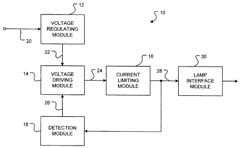
Referring now to Figure 1, a CCFL circuit 10 includes a voltage regulating
module 12, a voltage driving module 14, a current limiting module 16, and a
detection module 18. The voltage regulating module 12 receives an input
voltage
signal 20 from a voltage source. For example, the voltage source may be any
suitable AC voltage source ranging from approximately 90V - 265V with a
frequency
ranging from 50 Hz to 400 Hz. The voltage regulating module 12 generates an
output voltage signal 22. The output voltage signal 22 is substantially
constant
regardless of the value of the input voltage signal 20. In other words, the
value of
the output voltage signal 22 is substantially independent from the value of
the input
voltage signal 20. For example, in the preferred embodiment, the voltage
regulating
module 12 generates a constant output voltage signal 22 of 400V. However,
those
skilled in the art can appreciate that other suitable output voltage values
may be
used according to circuit performance requirements.
The voltage driving module 14 receives the output voltage signal 22 from the
voltage regulating module 12. Additionally, the voltage driving module 14 is
in
communication with detection module 18. The voltage driving module 14 receives
a
detection signal 26 from the detection module 18. The voltage driving module
14
CA 02544774 2006-04-24
generates a driving voltage signal 24 according to the output voltage signal
22 and
the detection signal 26. For example, the output voltage signal 22 determines
an
amplitude of the driving voltage signal 24. In one implementation, the voltage
driving
module 14 is a half-bridge driver as is known in the art. In this manner, the
waveform of the driving voltage signal 24 is maintained at a specific polarity
and
frequency.
The current limiting module 16 receives the driving voltage signal 24 from the
voltage driving module 14. The current limiting module 16 generates a current
supply signal 28 according to the driving voltage signal 24. A lamp interface
module
30 receives the current supply signal 28 from the current limiting module 16.
In
other words, the current limiting module 16 supplies current to power the lamp
interface module 30 via the current supply signal 28. The current limiting
module 16
maintains the current supply signal 28 at a constant value when the driving
voltage
24 is a constant value. As described above, the voltage regulating module 12
and
~ the voltage driving module 14 operate to ensure that the driving voltage
signal 24 is
a constant value. Therefore, the current supply signal 28 is a constant value
regardless of the value of the input voltage signal 20. Further, the current
supply
signal 28 is constant regardless of load requirements of the lamp interface
module
30. In the preferred embodiment, the current supply signal 28 is approximately
160
milliamps (mA). However, those skilled in the art can appreciate that other
suitable
current values may be used according to requirements of the lamp interface
module
30.
6
CA 02544774 2006-04-24
The detection module 18 communicates with the current supply signal 28
and/or the lamp interface module 30 to determine an operating condition of the
lamp
interface module 30. For example, although the current supply signal 28 is
constant,
the load requirements (i.e. impedance) of one or more lamps of the lamp
interface
module 30 affect the voltage of the lamp interface module 30. Therefore, as an
impedance of a lamp increases, the voltage across the lamp increases. The
impedance of the lamp may be indicative of length or other characteristics of
the
lamp.
In this manner, the detection module 18 is able to determine if an improper
lamp (i.e. a lamp of improper size) is being used with the lamp interface
module 30
based on a voltage increase. Similarly, the detection module 18 is able to
determine
if a lamp is missing from the lamp interface module 30, resulting in an open
circuit.
In another possible condition, all lamps associated with the lamp interface
module
30 may be present but damaged or burnt out, causing a voltage increase. Here
again, the detection module 30 is able to detect such a condition. In the
preferred
embodiment, the detection module 18 senses a voltage increase due one of the
above conditions and generates the detection signal 26 in response to the
voltage
increase. In other words, the detection signal 26 is indicative of one or more
operating conditions of the lamp interface module 30. If the detection signal
26
indicates that the voltage increases above a threshold, the voltage driving
module 14
shuts off the driving voltage signal 24 to prevent damage to the lamp
interface
module 30 or other elements of the CCFL circuit 10.
7
CA 02544774 2006-04-24
Referring now to Figure 2, the voltage regulating module 12, the voltage
driving module 14, the current limiting module 16, the detection module 18,
and the
lamp interface module 30 of one implementation of the CCFL circuit 10 are
shown in
detail. The voltage regulating module 12 receives the input voltage signal 20
and
generates the constant output voltage signal 22 as described above. Generally,
an
inductor 40 regulates the output voltage signal 22. The voltage regulating
module
12 also includes a power factor pre-regulator 42 and a VCC-regulating zener
diode
44 and transistor 46. The voltage regulating module 12 therefore provides
power
factor correction for the input voltage signal 20. The zener diode 44 and the
transistor 46 provide regulation for a VCC input 48 of the power factor pre-
regulator
42 and for a VCC signal 50 supplied to other components of the CCFL circuit
10.
For example, the voltage driving module 14 receives the VCC signal 50. Both
the
power factor pre-regulator 42 and the voltage driving module 14 require that
the
VCC signal 50 is within a particular range. Therefore, the zener diode 44 and
the
transistor 46 regulate the VCC signal 50 to ensure that the components that
receive
the VCC signal 50 operate properly.
The voltage driving module 14 includes a half-bridge driver 52 and timing
resistors 54-1, 54-2, and 54-3, referred to collectively as timing resistors
54. The
timing resistors 54 are connected across timing inputs 56 and 57 of the half-
bridge
driver 52 and determine a frequency of the driving voltage signal 24. The
driving
voltage signal 24 alternates between 400V and ground at the frequency
determined
by the timing resistors 54. In the present implementation, the frequency of
the
driving voltage signal 24 decreases as a resistance across the timing inputs
56 and
8
CA 02544774 2006-04-24
57 increases. Those skilled in the art can appreciate that any suitable
combination
of resistors can be used to determine a desired frequency.
The current limiting module 16 includes an inductor 58. The inductor 58
regulates the current supply signal 28. In the present implementation, the
inductor
58 has an inductance of approximately 4.7 millihenries in order to regulate
the
current supply signal 28 at 160 mA according to the 400V output voltage signal
22.
The lamp interface module 30 includes transformers 60 and 62 and lamp
sockets 64 and 66. The voltage and frequency of the driving voltage signal 24
supplied to the inductor 58 determines the current input to the transformers
60 and
62. More specifically, IPP = V l(4 * L * F) , where I pP is the peak-to-peak
input current
of the transformers 60 and 62 (i.e. the current supply signal 28), V is
voltage of the
driving voltage signal 24, L is the inductance of the inductor 58, and F is
the
frequency of the driving voltage signal 24.
The transformers 60 and 62 step down the current supply signal 28. In the
present implementation, the current at the outputs of the lamp sockets 64 and
66 is
approximately 8 mA. Although two transformers and corresponding lamp sockets
are shown, it is to be understood that any suitable number of lamp sockets may
be
provided. In the present implementation, each transformer 60 and 62 is
connected
independently to the lamp sockets 64 and 66, respectively. In other words,
each
transformer 60 and 62 includes separate primary and secondary windings, rather
than sharing a primary winding with the other transformer. The transformer 60
acts
as a first current source for the lamp socket 64. Similarly, the transformer
62 acts as
a second current source for the lamp socket 66. Since the primary windings of
the
9
CA 02544774 2006-04-24
transformers 60 and 62 are in series, the current through each transformer 60
and
62 is substantially identical. The output (i.e. secondary winding) of the
transformers
60 and 62 are isolated, thereby isolating operating conditions of the lamp
sockets 64
and 66 from one another. Changes in an impedance of a lamp connected to the
lamp socket 64 do not affect the operation of the lamp socket 66. Analogously,
changes in an impedance of a lamp connected to the lamp socket 66 do not
affect
the operation of the lamp socket 64. In this manner, the current supply signal
28 is
able to power either of the lamp sockets 64 and 66 when the other is not
functioning
properly.
As described above with respect to Figure 1, a voltage increase occurs when
the lamps connected to both of the lamp sockets 64 and 66 are burnt out or
otherwise not functioning properly, or when a lamp is missing. The detection
module
18 detects the voltage increase. More specifically, the detection module 18
includes
one or more voltage sensing devices. When a voltage at the voltage sensing
device
exceeds a particular threshold, the voltage driving module 14 shuts off the
driving
voltage signal 24 as described below in more detail.
The detection module 18 includes transistors 70 and 72, a comparator 74,
and a latching resistor 76. During normal operating conditions, the transistor
70 is
OFF, and no current flows between nodes 80 and 82 of the transistor 70. As
such,
the transistor 70 does not provide current to node 84 of the transistor 72,
and there
is no electrical communication between the transistor 72 and the timing input
57.
When the voltage at node 86 exceeds the threshold, the transistor 70 is ON. In
the
present implementation, the threshold is 2.5V. The VCC signal 50 (13.5 V in
the
CA 02544774 2006-04-24
present implementation) is applied through the transistor 70 to node 84,
through the
transistor 72, and to the timing input 57. The timing input 57 of the voltage
driving
module 14 also functions as a shutoff input. When the voltage at the timing
input 57
exceeds a threshold, the voltage driving module 14 interrupts the driving
voltage
signal 24.
Those skilled in the art can appreciate that certain components of the CCFL
circuit 10, and in particular the detection module 18, may be replaced with
electrical
components having analogous functions without departing from the features of
the
invention. For example, the transistor 72 may be replaced with a first diode
and a
second diode that are connected between nodes 84, 88, and 90. The anodes of
the
first and second diode are connected together at node 84.
In a further feature of the invention, current flows through the transistor 72
between nodes 84 and 88 when the transistor 70 is on. The VCC signal 50 is
applied to the comparator 74 through the latching resistor 76. In other words,
the
transistors 70 and 72 and the latching resistor 76 provide a positive voltage
via the
VCC signal 50 to the comparator 74. In this manner, the detection module 18
maintains the voltage at the timing input 57 at a level such that the voltage
driving
module 14 is OFF. To resume normal operation, the input voltage signal 20 of
the
CCFL circuit 10 must be reset or cycled.
Referring now to Figure 3A, an output current waveform 100 of the of the
CCFL circuit 10 is shown. The output current waveform 100 demonstrates the
output current at the lamp socket 64 when a first lamp connected to the lamp
socket
64 is 24 inches long and a second lamp connected to the lamp socket 66 is 14
11
CA 02544774 2006-04-24
inches long. Referring now to Figure 3B, an output current waveform 102
demonstrates the output current at the lamp socket 66 with the same
configuration
as described in Figure 3A. As shown in Figures 3A and 3B, the output currents
at
the lamp sockets 64 and 66 are substantially identical regardless of lamp
length.
For both waveforms 100 and 102, a 115 VAC, 60 Hz input voltage signal 20 was
used.
Referring now to Figure 4A, an output current waveform 104 of the CCFL
circuit 10 is shown. The output current waveform 104 demonstrates the output
current at the lamp socket 64 when a first lamp connected to the lamp socket
64 and
a second lamp connected to the lamp socket 66 are both 24 inches long.
Referring
now to Figure 4B, an output current waveform 106 demonstrates the output
current
at the lamp socket 64 when a first lamp connected to the lamp socket 64 is 24
inches long and the second lamp socket 66 is short circuited. Referring now to
Figure 4C, an output current waveform 108 demonstrates the output current at
the
lamp socket 66 when a first lamp connected to the lamp socket 64 is 24 inches
long
and the second lamp socket 66 is short circuited. As shown in Figures 4A, 4B,
and
4C, the output currents at the lamp sockets 64 and 66 are substantially
identical
regardless of lamp length. Further, a short circuit condition at either lamp
socket 64
or 66 does not affect the output current. For all waveforms 104, 106, and 108,
a 115
VAC, 60 Hz input voltage signal 20 was used.
Referring now to Figure 5, an input current waveform 110 of the CCFL circuit
is shown. The input current waveform 110 demonstrates the input current at the
input voltage signal 20 when a first lamp connected to the lamp socket 64 is
24
12
CA 02544774 2006-04-24
inches long and a second lamp connected to the lamp socket 66 is 14 inches
long.
In this manner, it can be seen that the input current is a continuous 60 Hz
sine wave
regardless of lamp length as a result of the power factor correction features
of the
invention. For the input current waveform 110, a 115 VAC, 60 Hz input voltage
signal 20 was used. Those skilled in the art can appreciate that the
configurations
demonstrated in Figures 3-5 are merely exemplary, and that the present
invention
can be extended to any number of configurations.
The description of the invention is merely exemplary in nature and, thus,
variations that do not depart from the gist of the invention are intended to
be within
the scope of the invention. Such variations are not to be regarded as a
departure
from the spirit and scope of the invention.
13