Note: Descriptions are shown in the official language in which they were submitted.
CA 02544792 2006-05-04
WO 2005/048181 PCT/US2004/036804
RFID TAG WITH ENHANCED READABILITY
BACKGROUND OF THE INVENTION
1. Field of the Invention
[0001] This invention relates to the field of Radio Frequency Identification
(RFID) tags and labels, and in particular to tags and labels that include an
antenna structure.
2. Description of the Related Art
(0002] Current inventory and manufacturing methods rely on the ability to
track
and identify items of concern, such as inventory items, packages, individual
parts,
etc., and to communicate information concerning such items of concern in a
wireless manner for processing and use. One known method of tracking and
providing information on such items of concern is to attach to each such item
a
wireless communication device, such as an active or passive transponder,
incorporated into an identification tag or label that responds to radio
frequency
interrogation and commands. The tag may store or represent information
concerning the object to which it is attached, such as a unique identifying
number,
object status such as opened or unopened, location, and the like. The tag may
be attached to an individual item or to packaging containing multiple items.
[0003] One example of a prior art RFID device 1 is illustrated in Fig. 1. The
device 1 includes a chip 2 coupled to a simple dipole antenna structure 3. The
antenna structure 3 consists of a pair of antenna elements 4 and 5 on a
substrate
6.
[0004] One difficulty with the simple dipole antenna structure 3 illustrated
in Fig.
1 is that the readability of the structure maybe highly dependent on its
orientation. For instance, readability of the device 1 along its edges,
especially
parallel to the direction of the antenna elements 4 and 5, along a narrow
'axis 8 of
the device 1, may be difficult.
(0005] It will be appreciated that it would be desirable to have RFID devices
that
overcome the previously-mentioned difficulties.
CA 02544792 2006-05-04
WO 2005/048181 PCT/US2004/036804
SUMMARY OF THE INVENTION
[0006] According to an aspect of the invention, an RFID device includes a
hybrid
loop-slot antenna.
[0007] According to another aspect of the invention, an RFID device includes:
an antenna structure having electrically conductive material on both sides of
an
elongated slot; a wireless communication device having a pair of contacts
electrically coupled to respective parts of the conductive material. The parts
of
conductive material are electrically coupled together at an end of the
elongated
slot distal from the wireless communication device.
[0008] According to yet another aspect of the invention, an RFID device has a
continuous layer of conductive material with an elongated slot therein; and an
RFID interposer with respective different contact points electrically coupled
to the
conductive material on the two sides of the elongated slot.
[0009] According to still another aspect of the invention, a method of
communicating with one or more of plural RFID devices, the method comprising:
enhancing performance of the devices by bringing the devices in close
proximity
to one another; and communicating with wireless communication devices of the
one or more of the devices.
[0010] According to a further aspect of the invention, performance of RFID
devices is enhanced by the devices being brought in close proximity to one
another.
[0011] To the accomplishment of the foregoing and related ends, the invention
comprises the features hereinafter fully described and particularly pointed
out in
the claims. The following description and the annexed drawings set forth in
detail
certain illustrative embodiments of the invention. These embodiments are
indicative, however, of but a few of the various ways in which the principles
of the
invention may be employed. Other objects, advantages and novel features of the
invention will become apparent from the following detailed description of the
invention when considered in conjunction with the drawings.
BRIEF DESCRIPTION OF THE DRAWINGS
[0012] In the annexed drawings, which are not necessarily according to scale,
[0013] Fig. 1 is an oblique view of a prior art device having a simple dipole
antenna structure;
CA 02544792 2006-05-04
WO 2005/048181 PCT/US2004/036804
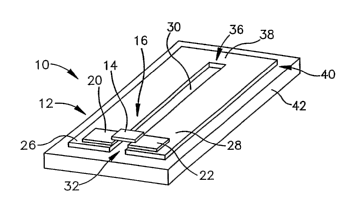
(0014] Fig. 2 is a plan view of an RFID device in accordance with the present
invention;
[0015] Fig. 3 is an oblique view of the RFID device of Fig. 2;
[0016] Fig. 4 is a plan view of an alternate embodiment RFID device in
accordance with the present invention;
[0017] Fig. 5 is a plan view of another embodiment RFID device in accordance
with the present invention;
[0018] Fig. 6 is a plan view of yet another alternate embodiment RFID device,
utilizing a monopole antenna;
[0019] Fig. 7 is a plan view of still another alternate embodiment RFID device
in
accordance with the present invention;
[0020] Fig..8 is an end view of the device of Fig. 7;
[0021 ] Fig. 9 is a side view of the device of Fig. 7;
[0022] Fig. 10A is a plan view of another alternate embodiment RFID device in
accordance with the present invention;
[0023] Fig. 10B is a side view of the device of Fig. 10A, with the substrate
of the
device folded along a fold line;
[0024] Fig. 11A is a plan view of another alternate embodiment RFID device in
accordance with the present invention;
[0025] Fig. 11 B is a side view of the device of Fig. 11A, with the substrate
of the
device folded along a fold line;
[0026] Fig. 12 is a plan view of yet another alternate embodiment RFID device
in accordance with the present invention;
[0027] Fig. 13 is a plan view of still another alternate embodiment RFID
device
in accordance with the present invention;
[0028] Fig. 14 is a plan view of another alternate embodiment RFID device in
accordance with the present invention;
[0029] Fig. 15 is an oblique illustrating yet another alternate embodiment
RFID
device in accordance with the present invention;
[0030] Fig. 16 is an oblique view illustrating one application for an RFID
device
of the present invention, attachment to a clothing item;
[0031] Fig. 17 is an oblique view of a reader display unit able to read RFID
devices of the present invention;
3
CA 02544792 2006-05-04
WO 2005/048181 PCT/US2004/036804
[0032] Fig. 18 is an oblique view of another reader display unit able to read
RFID devices of the present invention;
[0033] Fig. 19 is an oblique view illustrating reading of clothing items on a
portable rack;
[0034] Fig. 20 is an oblique view illustrating reading of clothing items on a
display rack;
[0035] Fig. 21A is an oblique view of multiple objects, each with an RFID
device,
in close proximity, in a carton or container;
[0036] Fig. 21 B is an oblique view of multiple objects, each with an RFID
device,
in close proximity, on a shelf;
[0037] Fig. 22A is an oblique view of a bottle with an RFID device on its
bottom
surface;
[0038] Fig. 22B is an oblique view layers of bottles with RFID devices;
[0039] Fig. 22C is an oblique view of a part of a bottle with an RFID device
on its
cap;
[0040] Fig. 22D is an oblique view of cylindrical bottles with RFID devices
thereupon;
[0041] Fig. 22E is an oblique view of rectangular bottles with RFID devices
thereupon;
[0042] Fig. 23 is a plan view of an RFID device with an antenna structure of a
first configuration;
[0043] Fig. 24 is a plan view of an RFID device with an antenna structure of a
second configuration;
[0044] Fig. 25 is a plan view of an RFID device with an antenna structure of a
third configuration;
[0045] Fig. 26 is a plan view of an RFID device with an antenna structure of a
fourth configuration;
[0046] Fig. 27 is a plan view of an RFID device with an antenna structure of a
fifth configuration;
[0047] Fig. 28 is a plan view of an RFID device with an antenna structure of a
sixth configuration;
[0048] Fig. 29 is a plan view of an RFID device with an antenna structure of a
seventh configuration;
4
CA 02544792 2006-05-04
WO 2005/048181 PCT/US2004/036804
[0049] Fig. 30 is a plan view of an RFID device with an antenna structure of
an
eighth configuration;
[0050] Fig. 31 is a plan view of an RFID device with an antenna structure of a
ninth configuration; and
[0051] Fig. 32 is a plan view of an RFID device with an antenna structure of a
tenth configuration.
DETAILED DESCRIPTION
[0052] A radio frepuency identification (RFID) device includes a conductive
antenna structure having an elongated slot therein. Parts of the antenna
structure on both sides of one end of the elongated slot are coupled to a
wireless
communication device, such as an RFID chip or interposes. On the opposite end
of the elongated slot, parts of the antenna structure at both sides of the
elongated
slot are electrically coupled together, for instance by being coupled together
by
other conductive parts of the antenna structure. All of the parts of the
antenna
structure may be parts of a continuous unitary layer of conductive material.
The
antenna structure with the elongated slot therein may facilitate increased
readability of the RFID device, particularly in directions out from the edges
of the
RFID device. The antenna structure may be directly conductively coupled to the
wireless communication device. Alternatively, the antenna structure may be
indirectly (reactively) coupled to the RFID device, such as by capacitive
coupling.
[0053] Referring initially to Figs. 2 and 3, an RFID device 10 includes an
antenna structure 12 that is coupled to a wireless communication device, such
as
an RFID chip 14 that may be a part of an RFID interposes or strap 16. The RFID
interposes or strap 16 includes conductive leads 20 and 22 that are coupled to
arms or parts 26 and 28 of the antenna structure 12.
[0054] The standard elements of the interposes or strap 16 include the RFID
chip 14 and conductive leads. The interposes or strap 16 also may include a
substrate to support the RFID chip 14 and the conductive leads. In most
embodiments herein (e.g. Figures 2 and 3) there is no substrate, but rather
the
conductive leads and the chip 14 are supported by the antenna. In the
embodiments of Figures 10A and 11A (discussed below), the interposes substrate
is the same as the antenna substrate. In another possible variation, the RFID
chip and the conductive leads may be supported by a separate substrate for
CA 02544792 2006-05-04
WO 2005/048181 PCT/US2004/036804
processing purposes, and this separate substrate may remain with the chip and
leads after the chip and leads are coupled to the antenna, or may be removed.
[0055] The arms 26 and 28 are on either side of an aperture or elongated slot
30, an opening between the parts of the antenna structure 12. At a first end
32 of
the aperture or elongated slot 30, an open end, the arms 26 and 28 are
electrically coupled to the conductive leads 20 and 22 of the RFID interposer
or
strap 16. The conductive leads 20 and 22 are in turn coupled to contact points
of
the RFID chip 14. At a second end 36 of the aperture or slot 30, a closed end
that is distal relative to the RFID interposer or strap 16, the arms 26 and 28
are
electrically connected together, for example by linked together by a
conductive
connection 38 that is also part of the antenna structure 12. The arms 26 and
28,
and the conductive connection 38, all may be parts of a unitary, continuous
layer
40 of conductive material forming the antenna structure 12. The conductive
layer
40 may be attached or otherwise coupled to a substrate 42.
[0056] The slot or aperture 30 may have a substantially constant width between
the arms 26 and 28 of the antenna structure 12. The slot 30 may have a length
from of approximately one quarter of a wavelength of radiation used to
communicate with the RFID chip 14. The slot 30 allows the RFID device 10 to be
read along a narrow axis 46. Indeed, the RFID device 10 may exhibit good
readability characteristics in substantially any direction within or parallel
to the
plane of the antenna structure 12 or the RFID device 10 as a whole.
[0057] In addition, at short ranges, the RFID device 10 demonstrates good read
performance in other directions, such as above and below the tag. Thus the
RFID device 10 shows good read performance in all directions around the device
10. The read performance of the RFID device 10 is good even when the device
is of a small size. For example, an RFID device of the configuration shown in
Figs. 2 and 3, having outer dimensions of 25mm x 25mm (1 inch x 1 inch) has
been found to have good read performance at distances in excess of 2m (6.5
feet), when utilizing suitable power and frequency levels. Examples of
suitable
power and frequency labels are operation over a frequency band of 902 to
928MHz at a power of 4W e.i.r.p (effective isotropic radiated power) in
accordance with FCC part 15 section 247. By using a suitable reader with
either
a circularized polarized antenna, or dual linear antennas polarized at 90
degrees
to each other connected to separate ports on a reader system which are
CA 02544792 2006-05-04
WO 2005/048181 PCT/US2004/036804
alternately switched, the antenna structure 12 gives a read capability that is
good
over a wide variety of orientations, and may be substantially orientation
independent.
(0058] The coupling between the RFID chip 14 and the arms 26 and 28 may
either be a direct conductive coupling, occurring through the conductive leads
20
and 22 of the interposer 16, or may be in whole or in part a reactive
coupling,
such as capacitive or inductive coupling through a dielectric material.
Several
configurations of reactive coupling connections are discussed below with
regard
to different embodiments of the RFID device 10. With regard to the direct
(conductive) electrical connections between the conductive leads 20 and 22,
and
the arms 26 and 28, such connections may be made by use of a suitable
conductive adhesive.
(0059] A circuit path 54 proceeds from one side (contact point) of the RFID
chip
14, through the arm 26, the conductive connection 38, and the arm 28, to
another
side (contact point) of the RFID chip 14. Thus, in contrast to a standard slot
antenna, there is not conductive material fully around the slot 30. A standard
slot
antenna has a short circuit of conductive material fully surrounding a slot.
[0060] The antenna structure 12 of the RFID device 10 may have some features
of loop antennas, and may have some features of slot antennas, while
overcoming the null spots that may occur in traditional loop antennas and slot
antennas. The antenna structure 12 may provide better coverage of a wide range
of orientations by coupling to the RFID chip 14 with at least two modes of
operation. The antenna modes may include two or more modes that include
modes such as a mode substantially that of a notch antenna, a mode
substantially that of a loop antenna, a mode substantially that of a folded
dipole
antenna, and/or a mode substantially that of a slot antenna.
[0061] The RFID device 10 may utilize a variety of suitable materials. The
substrate 42 may be a suitable plastic material, such as PET or polypropylene,
which may be a flexible film or sheet of plastic material. The conductive
layer 40
of the antenna structure 12 may be formed, deposited or adhered onto the
substrate 42 by any of a variety of suitable methods. For example, the
conductive layer 40 may be a conductive ink, such as an ink containing metal
particles, that is printed onto the substrate 42 in a suitable pattern.
Alternatively,
the conductive layer 40 may be plated onto the substrate 42, such as by
CA 02544792 2006-05-04
WO 2005/048181 PCT/US2004/036804
electroplating. As another alternative, the conductive layer 40 may be
adhesively
adhered to the substrate 42. Etching may be used to remove conductive material
to form the slot 30.
[0062] The RFID device 10 may include additional suitable layers, such as
protective layers to protect the functional elements of the device that may
also
provide desired surface properties such as printability or weatherability,
and/or an
adhesive layer to adhere the device 10 to an object.
[0063] It will be appreciated that a variety of wireless communication
devices,
such as RFID interposers or straps, may be used as the RFID interposes or
strap
16. Examples of suitable RFID interposers or straps include an RFID strap
available from Alien Technologies, and the interposes (called a module)
marketed
under the name I-CONNECT, available from Philips Electronics. Chips available
from Alien Technologies may be attached either conductively, in a flip-chip
die, or
conductively or reactively for a strap form of the chip. Suitable RFID chips
include
Philips HSL chip, available from Philips Electronics, and the EM Marin EM4222,
available from EM Microelectronic-Marin SA, as well as RFID chips available
from
Matrics Inc. of Columbia, Maryland USA.
(0064] It will be appreciated that the RFID device 10 may have any of a
variety
of suitable configurations, some of which are described further below. The
configuration of the conductive areas and slot of the antenna structure may
vary
widely, for instance. As one example, the slot 30 may be substantially
rectangular, as shown in Figs. 2 and 3. Alternatively, the slot may have
another
shape, such as bent or curved.
(0065] Fig. 4 shows one alternative configuration for the RFID device 10, in
which the slot 30 has a bent shape, with a number of constant-width segments
60, 62, 64, and 68, angled with regard to one another. The segments 60-68
allow
the same overall slot length on a small, more compact device. An RFID
interposes 16 is mounted onto both sides of the aperture or slot 30, thus
using
material of the conductive layer on both sides of the slot 30 and along a
distal end
of the elongated slot as a hybrid loop-slot antenna, similar to the above-
discussed
embodiment of the RFID device 10 shown in Figs. 2 and 3. The conductive layer
40 covers substantially all of an underlying substrate 42, with an exception
of the
slot 30.
CA 02544792 2006-05-04
WO 2005/048181 PCT/US2004/036804
[0066] Turning now to Fig. 5, another embodiment of the RFID device 10 is
shown, in which the arms 26 and 28 are not directly electrically coupled to
one
another. Rather the arms 26 and 28 are reactively coupled together by
respective coupling portions 76 and 78 of the arms 26 and 28, that are
capacitively coupled together across an interaction region 80 of the substrate
42
upon which the conductive arms 26 and 28 are mounted. The interaction region
80 and the slot 30 are to some extent separate, although it will be
appreciated
that the interaction region 80 may be taken into account when properly tuning
the
antenna structure 12 by tuning the arms 26 and 28 in the vicinity of the slot
30.
[0067] The embodiment of the RFID device 10 illustrated in Fig. 5 may be
advantageously used with RFID chips that require that no short circuit be
presented between the contacts of the chip that are coupled to the arms 26 and
28. Examples of such RFID chips are the EM4222 and the HSL chips.
[0068] Fig. 6 illustrates yet another embodiment of the RFID device 10, which
has an antenna structure 12 that includes both a hybrid loop-slot antenna, as
well
as a monopole antenna element 90. The hybrid loop-slot antenna may be similar
to the structure described above with regard to the embodiment shown in Figs.
2
and 3, with a pair of arms 26 and 28 coupled to different contact points of
the
RFID chip 14, and a conductive connection 38 between the arms 26 and 28, with
the conductive connection 38 and the arms 26 and 28 defining the slot 30. The
arms 26 and 28 are coupled, respectively, to an RF input 92 and a common
(ground) connection 94 of the RFID chip 14.
[0069] The monopole antenna element 90 is a folded dipole element 96 that is
electrically coupled to another contact point (connection) 100 of the RFID
chip 14.
The dipole element 96 has a serpentine shape, with a number of back-and-forth
segments 102. The antenna structure 12 thus utilizes the hybrid loop-slot
antenna as a ground plane for the folded dipole element 96. The antenna
structure 12 is thus a dual polarization antenna.
[0070] Fig. 7-14 show various embodiments of the RFID device 10 that have
capacitive coupling between the RFID chip 14 and at least one of the arms 26
and 28. Referring first to the embodiment of the RFID device 10 shown in Figs.
7-
9, the conductive leads 20 and 22 of the RFID interposer 16 are adhesively
coupled to the arms 26 and 28 of the antenna structure 12 by respective
adhesive
pads or layers 110 and 112. The adhesive pads 110 and 112 are made from a
CA 02544792 2006-05-04
WO 2005/048181 PCT/US2004/036804
non-conductive adhesive that prevents direct (conductive) electrical coupling
between the conductive leads 20 and 22, and the arms 26 and 28. Rather, the
conductive leads 20 and 22 are capacatively coupled to the arms 26 and 28
across the non-conductive adhesive pads 110 and 112. By avoiding direct
conductive electrical coupling between the conductive leads 20 and 22, and the
arms 26 and 28, shorting together of the corresponding contact points of the
RFID chip 14 is avoided. As noted above, some chips may require that the
contact points not be shorted together, for the chips to operate properly.
[0071] It will be appreciated that a suitable thickness may be selected for
the
adhesive pads 110 and 112, in order to provide the desired capacitive coupling
between the conductive leads 20 and 22, and the arms 26 and 28. The thickness
of the adhesive pads may be selected based on such factors as the operating
power and frequency, the coupling area, and the dielectric constant of the
adhesive to be used. In one example, adhesive pads having an area of 5mm2
and a thickness of 10pm may be used, although it will be appreciated that a
wide
range of suitable areas and thicknesses may be used.
[0072] Figs. 10A and 10B show another embodiment of the RFID device 10,
which illustrates one way of forming a device that utilizes adhesive pads 110
and
112 to attach conductive leads 20 and 22 to arms 26 and 28. As shown in Fig.
10A, different parts of the device 10 are formed on different parts 120 and
122 of
a substrate 124. The parts 120 and 122 have a fold line 126 therebetween. On
the first part 120 the RFID interposes 16 is placed, with the conductive leads
20
and 22 face up. The RFID interposes 16 may be attached to the first part 120
of
the substrate 124 by use of a suitable adhesive. Alternatively, the interposes
16
may be formed in situ, by depositing or forming the conductive leads 20 and
22,
such as by printing or electroplating, after placing the RFID chip 14 face up
on the
first part 120.
[0073] The antenna structure 12 is deposited or attached onto the second part
122 of the substrate 124. The adhesive pads 110 and 112 may then be
deposited on the arms 26 and 28 of the antenna structure 12, for example by a
suitable printing process.
[0074] Following making of the structure shown in Fig. 10A, the two parts of
the
device are joined together by folding the substrate 124 along the fold line
126.
This brings in conductive leads 20 and 22 into contact with the adhesive pads
110
to
CA 02544792 2006-05-04
WO 2005/048181 PCT/US2004/036804
and 112, thereby adhesively joining together the conductive leads 20 and 22 to
the arms 26 and 28, as illustrated in Fig. 10B.
[0075] The first part 120 of the substrate 124 may be sized to substantially
cover
the second part 122, when the first part 120 is folded over the second part
122.
The second part 122 may be pressed against and sealed to the second parts,
such as by heat sealing, to enclose and protect the operative elements of the
device 10.
[0076] It will be appreciated that the method of making an RFID device, as
illustrated in Figs. 10A and 10B, may be performed as a series of continuous
roll
operations, such as in a roll-to-roll process. The placement of the RFID chip
14
and/or the interposer 16; the formation of the antenna structure 12 on the
substrate 124 (or adherence of the antenna structure 12 to the substrate 124);
and/or placement of the adhesive pads 110 and 112, all may be performed as
roll
operations. Such operations may be performed on a web of material, which may
then be suitably cut to produce individual RFID devices.
[0077] It will be further appreciated that the sort of method described above
may
be utilized with RFID devices having other configurations, as described
herein.
For example, suitable electrically-conductive adhesive may be substituted for
non-conductive adhesive of the adhesive pads 110 and 112, thereby producing
an RFID device 10 where the conductive leads 20 and 22 are directly
(conductively) electrically coupled to the arms 26 and 28 of the antenna
structure
12. As another example, the antenna structure 12 may have some of the other
configurations described herein.
[0078] Figs. 11 A and 11 B illustrate another folded embodiment of the device
10,
with a first part 130 and a second part 132 of a substrate 134 being separated
along a fold line 136. The first part 130 has an RFID chip 14 and conductive
leads 20 and 22 thereupon. The second part 132 has the conductive layer 40,
with its various parts 26, 28, and 38, thereupon.
[0079] As illustrated in Fig. 11 B, the first part 130 may be folded back
along the
fold line 136, to make back-to-back contact with the second part 132 of the
substrate 134. The parts 130 and 132 may be joined with an adhesive layer 138.
In the resulting structure, the conductive leads 20 and 22 are capacitively
coupled
to the arms 26 and 28, with the combined thickness of the parts 130 and 132 in
between.
11
CA 02544792 2006-05-04
WO 2005/048181 PCT/US2004/036804
[0080] Turning now to Fig. 12, another embodiment of the RFID device 10 has
an interdigitated capacitive coupling 140 for coupling the RFID chip 14 (or an
RFID interposes) to the arm 26 of the antenna structure 12. The chip 14 is
conductively coupled to a conductive pad 142 on the substrate 42. The
conductive pad 142 includes a number of fingers 144 jutting out therefrom,
along
the substrate 42. The fingers 144 interdigitate with corresponding fingers 146
of
the arm 26, leaving a narrow serpentine gap 150 between the sets of fingers
144
and 146. Capacitive coupling may occur across the gap 150, indirectly
(capacitively) electrically coupling the conductive pad 142 and the arm 26,
without
danger of short-circuiting of the arm 26. The conductive pad 142 and the
fingers
144 may be part of a conductive layer 154 that also includes the arms 26 and
28,
and the conductive connection 38.
(0081] Fig. 13 shows an additional embodiment of an RFID device 10 that has
reactive coupling between the chip 14 and the arm 26. In the embodiment shown
in Fig. 13, the RFID chip 14 (or RFID interposes) is coupled to a conductive
element 160 that follows a curvy path through the arm 26, with a gap 162
between the conductive element 160 and the arm 26. This enables capacitive
coupling between the conductive element 160 and the arm 26.
(0082] Fig. 14 illustrates yet another capacitive coupling embodiment of the
RFID device 10. The device shown in Fig. 14 has the antenna structure 12 on an
opposite side of the substrate 42 from the RFID interposes 16. The conductive
leads 20 and 22 of the RFID interposes 16 are capacitively coupled with the
arms
26 and 28 of the antenna structure 12, across the portions of the substrate 42
therebetween.
[0083] A variety of capacitive coupling embodiments of the RFID device 10 have
been described above. It will be appreciated that other types of indirect
reactive
coupling, such as inductive coupling via a magnetic field, may be used
instead.
[0084] Fig. 15 illustrates an embodiment of the RFID device 10 with a
corrugated cardboard layer 180. A pair of conducting strips 182 and 184, such
as
copper strips, are placed on corrugations 186 and 188 during manufacture of
the
cardboard layer 180. The conducting strips 182 and 184 serve as the arms of a
hybrid loop/aperture antenna. A shorting conductive connection 190 is placed
at
one point along the conductive strips 182 and 184, and an RFID interposes 16
is
placed at another point along the conductive strips 182 and 184. The points
for
12
CA 02544792 2006-05-04
WO 2005/048181 PCT/US2004/036804
placement for the shorting connection 190 and the interposer 16 are chosen so
that the aperture 12 defined by the various elements has a suitable length.
[0085] Following placement of the elements of the device 10 shown in Fig. 15,
construction of the cardboard layer may be completed by placement of a facing
layer atop the corrugations. The cardboard may be used for suitable purposes,
such as in a carton or other container. The RFID device 10 thus may be
employed as an internal device within a cardboard layer, readable from a wide
variety of orientations. The placement of the device within the cardboard
layer
may help protect the device from physical damage during handling of the
cardboard. In addition, placement of the device within a cardboard layer helps
to
hide the device, protecting it from deliberate attempts to disable it.
However, it
will be appreciated that an external marker may be provided on the cardboard
to
indicate location of the RFID device 10, for example to aid in placement of a
reader for short-range reading.
[0086] Fig. 16 illustrates one application of the RFID device 10, with
application
of the device 10 to a clothing item 200, such as a shirt. The device 10 may be
a
card-mounted label placed between buttons of the clothing item 200, or
attached
to the item 200 with a plastic fastener. The device 10 on the clothing item
200
may be read with a hand-held reader 204, from any of a variety of directions
relative to the clothing item 200.
[0087] Fig. 17 shows a display unit 210 capable of reading RFID devices 10 on
a group of clothing items 200. The display unit 210 has a number of suitable
antennas 212 and 214 in a back wall 216 of the display unit 210. The antennas
212 and 214 are coupled to a reader 220. The ability of the RFID devices 10 to
be read along their edges in a variety of orientations, especially along axes
in the
narrow directions of the devices 10, facilitates reading of the devices by the
display unit 210.
[0088] It will be appreciated that the variety of permissible edge-reading
angles
for the devices 10 allow reading even when the items 200 are placed in the
display unit 210 at a variety of orientations, as illustrated in Fig. 18. The
flexibility
in variety of read orientation for the RFID devices 10 allows, for example, a
retailer flexibility to display the items 200 at a variety of orientations,
while still
allowing them to be detected by the display unit 210. In addition, detection
by the
13
CA 02544792 2006-05-04
WO 2005/048181 PCT/US2004/036804
display unit 210 may be maintained largely unaffected by how the items 200 are
placed or misplaced in the display unit, such as by employees or customers.
[0089] Fig. 19 illustrates reading of RFID devices 10 on clothing items 230,
which are on a portable rack 240. The RFID devices 10 may be integrated into
labels 232 on the clothing items 230. The devices 10 on the items 230 may be
read from a side direction 244 or 246 as the rack 240 is moved past a reading
station. The good edge-reading characteristics of the RFID devices 10
facilitate
detection of the devices 10 in the directions 244 and 246.
[0090] Fig. 20 shows the clothing items 230 mounted on a display rack 250.
The RFID devices 10 on the clothing items 230 may be read from a read
direction
252, from an antenna 254 on a back wall 256 of the display rack 250. Figs. 19
and 20 illustrate the usefulness of the quasi-isotropic read properties of the
RFID
device 10, allowing the clothing items 230 to be detected on a variety of
racks,
read from a variety of directions.
(0091] It will be appreciated that the read properties of the RFID devices 10
may
be utilized in detecting and/or tracking a wide variety of objects in addition
to
clothing items. The detection of the clothing items 200 and 230 is but one
example of a wide variety of objects with which the RFID devices 10 may be
utilized.
(0092] Turning now to Figs. 21A and 21 B, multiple objects 300, each with an
RFID device 10, are placed in close proximity to one another, such that the
proximity of the RFlD devices 10 to one another enhances performance of the
RFID devices 10. Fig. 21A shows the objects 300 placed in a carton or
container
310. Fig. 21 B shows the objects 300 placed on a shelf 320.
j0093] The term "close proximity," as used herein, refers to adjacent
(nearest) of
the RFID devices 10 being within about twice a relevant longest dimension of
conductive material (e.g., length or width) of the antenna of the RFID device
10.
A group of RFID devices 10 may be said to be in close proximity to one another
if
each of the RFID devices is in close proximity with at least one other device,
and
if all of the RFID devices are linked together by devices in close proximity
with
one another. For instance, if the antennas of the RFID devices 10 had a length
and width of about 5cm, the RFID device 10 may be in close proximity to one
another if they are within about 10cm of one another.
14
CA 02544792 2006-05-04
WO 2005/048181 PCT/US2004/036804
[0094] It is believed that having the RFID devices 10 in close proximity to
one
another improves the radiation resistance of the RFID devices 10. This
improves
the performance of the RFID devices 10, such as by increasing the read
distance
and/or signal strength for the RFID devices 10.
[0095] It will be appreciated that many advantages may be obtained by
increasing performance of the RFID devices 10 when the devices 10 are in close
proximity to one another. The increased performance of devices in close
proximity to one another may allow use of smaller RFID devices, while still
maintaining desired performance levels, at least when the devices are in close
proximity to one another. Smaller RFID devices 10 are desirable from a number
of standpoints: smaller RFID devices require less raw materials, which may
reduce costs; and smaller RFID devices require less space to affix to an
object,
are loss obtrusive, and are less likely to be damaged. In addition, smaller
RFID
devices may be less detectable after purchase by the end user, when the RFID
device 10 is no longer in close proximity to other such devices. The reduced
detectability of a separated RFID device (not in close proximity to other
devices)
may allay privacy concerns concerning RFID devices.
[0096] Increased performance of the RFID devices 10 may be particularly useful
in circumstances where the RFID devices 10 are naturally grouped together,
such
as when objects are shipped in containers or are displayed on shelf or in
other
ways. For instance, the shelf 320 may have or be near a reader 324 used to
keep track of available inventory.
[0097] The performance of the RFID devices 10 may also be enhanced by the
presence of electrically-conductive materials, other than those in the RFID
device
10. For instance, the objects 300, the container 310, and/or the shelf 320 may
contain the metal or other electrically-conductive material that may enhance
the
performance of the RFID devices 10.
[0098] The RFID devices 10 may have an overall size of about 8cm (3 inches) x
8cm (3 inches) or less. The RFID device 10 may be even smaller, having for
example a size of about 4cm x 4cm or less, or of about 2.5cm (1 inch) x 2.5cm
(1
inch) or less. However, it will be appreciated that other sizes for the RFID
devices
are possible.
[0099] From the definition of "close proximity" given above, it will be
appreciated
that there is a wide range of spacing of RFID devices 10 that will produce
is
CA 02544792 2006-05-04
WO 2005/048181 PCT/US2004/036804
enhanced performance of the RFID devices 10. For example, the RFID devices
may have enhanced performance when the nearest devices are within about
4cm of each other.
[0100] Generally, the enhancement of performance resulting by the close
proximity of the RFID devices 10 is increased the closer the devices 10 are to
one
another. This result is not to be expected from experiences with at least some
types of prior art antenna configurations, such as dipole antenna
configurations.
In contrast to the enhancement by close proximity described herein,
performance
of devices with dipole antennas actually degrades when the devices are brought
closely together, with nearby devices effectively "de-tuning" one another.
[0101] Figs. 21A and 21 B show the objects 300 in the container 310 and on the
shelf 320. It will be appreciated that objects with RFID devices may be placed
in
close proximity to one another in many other sorts of circumstances, including
other sorts of display devices and/or transport devices and/or configurations.
[0102] Generally it is observed in the case of RFID devices with hybrid
antennas
(combining characteristics of slot or notch antennas with characteristics of
loop
antennas) that the enhancement of performance is most pronounced if the tags
are in close proximity, and are coplanar.
[0103] This performance enhancement in grouping of tagged items may be
employed to advantage in the RFID tagging of packaged articles. Figs. 22A-22E
illustrate this effect in a variety of configurations of RFID-tagged, packed
bottles
330, with RFID devices 10 in close proximity to one another. In Fig. 22A the
bottles 330 are tagged at their the bottom surfaces 332 with RFID devices 10,
wherein packing the bottles 330 on a common surface results in roughly co-
planar placement of the RFID devices 10. Fig. 22B shows multiple layers of
tagged bottles 330 separated by packing sheets 336, resulting in a series of
co-
planar groups of RFID devices (horizontal planes at different packing levels).
In
Fig. 22C, the RFID devices 10 are applied to plastic bottle caps 340 instead
of to
the bottoms of the bottles. Placement of the RFID devices 10 on the bottle
caps
340 may be desirable for bottles containing liquids, in order to provide
greater
distance of the RFID device 10 from the liquid. In Figs. 22D and 22E the
bottles
330 are tagged at their sidewalls 350. For bottles 330 with cylindrical shapes
352
(Fig. 22D), this may result in less consistency in co-planarity of groups of
tags
because of variations in orientation from bottle to bottle. For bottles 300
with flat
16
CA 02544792 2006-05-04
WO 2005/048181 PCT/US2004/036804
faces 354 and natural orientations, such as rectangular cross sections 358
(Fig.
22E), it is easier to assure co-planarity of the RFID devices 10.
[0104] Figs. 22A-22E show RFID devices 10 placed on bottles 330. However, it
will be appreciated that the bottles 300 are merely examples of a larger group
of
objects that may have RFID devices 10 attached to or mounted thereupon.
[0105] Figs. 23-32 show several possible alternative configurations for the
antenna structure 12 of the RFID device 10. Fig. 23 shows an antenna structure
12a having a rectangular shape, with a straight slot 30a having a wider
portion
400 close to an RFID interposes 16a, and a narrower portion 402 further from
the
interposes 16a.
[0106] Figs. 24 and 25 show antenna structures 12b arid 12c that both have
square shapes, with respective diagonal slots 30b and 30c. The slot 30b is a
straight slot, running from one corner of the antenna structure 12b, through
the
center of the structure, and most of the way to the opposite corner. The slot
12c
is an angled slot, with a bend 410 at a center of the antenna structure 12c.
[0107] Figs. 26-29 show various antenna structures 12d-12g with non-straight
slots 30d-30g. The slot 30d has a pair of curved sections 420 and 422. The
slots
30e-30g have various angled bends 426 in them. The antenna structures 12d-12f
have a generally circular shape, while the antenna structure 12g has a square
shape.
[0108] Fig. 30 shows an antenna structure 12h with a square shape, and having
a C-shape slot 30h. The slot 30h has a branch 430 is coupled to one of the
distal
legs 432 of the C-shape slot 30h. The RFID interposes 16 is coupled across the
branch 432.
[0109] Fig. 31 shows an antenna structure 12i that has a compensation element
440 that aids in compensating for electrical characteristics of nearby objects
(e.g.,
electrical conductive and dielectric constant), so as to provide performance
that is
less dependent upon the characteristics of nearby objects. Many other sorts of
compensation elements are described and illustrated in U.S. Provisional Patent
Application No. 60/536,483, filed January 20, 2004, which is incorporated
herein
by reference in its entirety.
[0110] Fig. 32 shows an antenna structure 12j that includes a pair of portions
450 and 452 that are separated by a narrow gap 454. The portions 450 and 452
may be capacitively coupled across the gap 454. A straight slot 30j fully
1~
CA 02544792 2006-05-04
WO 2005/048181 PCT/US2004/036804
separates parts 456 and 458 of the portion 450, and partially bisects the
portion
452.
[0111] Although the invention has been shown and described with respect to a
certain embodiment or embodiments, it is obvious that equivalent alterations
and
modifications will occur to others skilled in the art upon the reading and
understanding of this specification and the annexed drawings. In particular
regard to the various functions performed by the above described elements
(components, assemblies, devices, compositions, etc.), the terms (including a
reference to a "means") used to describe such elements are intended to
correspond, unless otherwise indicated, to any element which performs the
specified function of the described element (i.e., that is functionally
equivalent),
even though not structurally equivalent to the disclosed structure which
performs
the function in the herein illustrated exemplary embodiment or embodiments of
the invention. In addition, while a particular feature of the invention may
have
been described above with respect to only one or more of several illustrated
embodiments, such feature may be combined with one or more other features of
the other embodiments, as may be desired and advantageous for any given or
particular application.
is