Note: Descriptions are shown in the official language in which they were submitted.
CA 02544935 2006-05-04
WO 2005/052974 PCT/US2004/032801
MANUFACTURING PROCESS OF SUBSTRATE FOR IMAGE DISPLAY PANEL
Background
A panel-shaped image display apparatus includes a liquid crystal (LC) display
panel, an organic electroluminescence (EL) display panel, a plasma display
panel ("PDP"),
and so forth. Particularly, a PDP is characterized by being thin and capable
of providing a
large display, for industrial purposes and recently for use as a wall-hung TV.
Generally, a
' PDP has a number of small discharge display cells as shown schematically in
Fig.l . In a
PDP 50, each discharge display cell 53 is surrounded and defined by a pair of
glass
substrates separated from and opposed to each other, that is, a front glass
substrate 61 and
a back glass substrate 51, and ribs (also referred to as burner ribs,
partition walls or burner
walls) 54 having a fine structure arranged in a predetermined pattern between
these glass
substrates. The front glass substrate 61 comprises a transparent display
electrode 63
consisting of scan electrodes and sustain electrodes, a transparent dielectric
layer 62 and a
transparent protective layer 64 thereon. The back glass substrate 51 comprises
an address
electrode 53 and a dielectric layer 52 thereon. Each discharge display cell 56
has a
phosphor layer 55 on the inner wall and at the same time a rare gas (for
example, Ne-Xe
gas) is enclosed for a self light-emitting display by a plasma discharge
between the above-
mentioned electrodes.
In general, the rib 54 has a ceramic fine structure and is normally provided
on the
back glass substrate 51 together with the address electrode 53, making up a
back plate for
a PDP, as shown schematically in Fig.2: As the shape and the dimensional
precision of the
rib 54 considerably affect the performance of a PDP, it is formed in various
patterns. A
typical one is a stripe rib pattern 54 shown in Fig.2, and in this case, each
discharge
display cell 56 also has a stripe pattern.
Particularly, in the substrate for a PDP as described above, an electrode is
generally formed from a conductive electrode material such as silver by use of
the
photolithographic method or the screen-printing method. For example, the
formation of a
silver electrode by use of the photolithographic method is carried out by
performing a
series of processes of exposing with a photo-mask, developing and drying after
coating a
photosensitive silver paste on the entire surface of a glass substrate, and by
curing the
silver paste by sintering. On the other hand, the formation of a silver
electrode by use of
CA 02544935 2006-05-04
WO 2005/052974 PCT/US2004/032801
the screen printing method, which is a more simplified method, is carned out
by drying in
a drying oven after screen-printing a silver paste designed for printing in a
fixed pattern
directly on a glass substrate, and by curing the silver paste by sintering.
Ribs for a PDP substrate are generally formed by use of a screen printing
method,
a sand blast method, a transfer method, and so forth, after forming electrodes
on a glass
substrate as described above. For example, the formation of ribs by use of the
transfer
method is carried out by performing the processes of filling the recess in a
mold sheet
having a printing mask in accordance with the shape of the rib with a ceramic
paste;
contacting the mold sheet closely to the glass substrate; peeling off the mold
sheet and
transferring the ceramic paste from the sheet recess onto the glass substrate;
curing the
ceramic paste by sintering.
However, when manufacturing a PDP substrate equipped with ribs and electrodes
by use of the above-mentioned methods, at least three heating processes, that
is, a drying
process and a sintering process during an electrode formation stage and a
sintering process
during a rib formation stage, are utilized that consume substantial amounts of
energy and a
large amount of equipment investment. It has been suggested in the prior art
to form ribs
and electrodes simultaneously or reduce the number of heating steps.
For example, a method for manufacturing a PDP substrate has been proposed,
that
is characterized in that after a rib forming mold is bonded and fixed to an
insulating
substrate with an electrode composition, the recess in the rib forming mold is
filled with a
rib material and solidified, and then is sintered integrally with the
insulating substrate at a
temperature of 500 to 650°C for forming ribs and electrodes
simultaneously (JP 10-
241581).
On the other hand, a method for manufacturing a back plate for a PDP has been
proposed, that is characterized in that at least one of a rib forming part
consisting of a rib
precursor mixture and an electrode pattern including an electrode material,
and a
multicolor pattern including a phosphor are baked in a state in which they are
formed on a
substrate in a prescribed arrangement (JP 10-334793).
Moreover, amethod for manufacturing a substrate for a PDP has been proposed,
that is characterized in that after electrode patterns are formed on a glass
substrate by use
of a paste for the electrodes, and a dielectric material paste applied layer
is formed by
applying a dielectric material paste thereon, and fiu-ther a rib pattern is
formed by use of a
2
CA 02544935 2006-05-04
WO 2005/052974 PCT/US2004/032801
paste for rib thereon, the rib pattern is baked together with the electrode
patterns and the
dielectric material paste applied layer (JP 11-329236).
Another method for manufacturing a PDP has been proposed, that is
characterized
by comprising a first process in which a thick film pattern material of an
electrode is
formed by use of a first type roller, and a second process in which a thick
film pattern
material of a rib is formed by use of a second type roller (JP 001-35363)
Summary of the Invention
The methods just describe employ at least two heating processes. Also these
methods utilize relatively large equipment having a complex structure.
Described herein is a manufacturing process of a substrate for an image
display
panel comprising a transparent substrate and protruding ribs and thin film
electrodes each
formed in the predetermined pattern on the surface of the substrate,
characterized by
comprising steps of: forming an electrode precursor layer by coating an
electrode
precursor on the surface of the substrate' in the predetermined pattern;
forming a rib
precursor layer in the predetermined pattern on the surface of the substrate
on which the
electrode precursor layer has been formed; and sintering the electrode
precursor layer and
the rib precursor layer simultaneously at a predetermined temperature.
The method reduces the number of process steps by reducing the number of
heating step to one-step, thereby reducing energy consumption and equipment
investment,
when manufacturing a PDP substrate equipped with ribs and electrodes or other
substrates
for use in an image display panel.
Further, it is possible to manufacture ribs highly precisely without the
occurrence
of bubbles and defects such as pattern deformation, particularly by use of the
transfer
method for forming ribs.
Furthermore, it is possible to manufacture ribs having a complex structure
with
high dimensional precision without requiring skill and easily carry out
peeling from the
forming mold without damages to the ribs.
Brief Description of the Drawings
Fig. 1 is a sectional view of an illustrative PDP.
Fig. 2 is a perspective view of a back plate for a PDP used in the PDP in
Fig.l .
3
CA 02544935 2006-05-04
WO 2005/052974 PCT/US2004/032801
Fig.3 shows sectional views illustrating a manufacturing process of a
substrate for
a PDP of the present invention.
Fig.4 shows sectional views illustrating the barner rib forming process in the
manufacturing process of a substrate for a PDP in Fig.3.
Detailed Description of Preferred Embodiments
The manufacturing process of a substrate for an image display panel according
to
the present invention is particularly suitable to manufacture a substrate
comprising a
transparent substrate and protruding ribs and thin film electrodes formed in a
predetermined pattern, respectively, on the surface of the substrate. A
substrate having
such a structure includes a substrate for an image display panel such as an LC
display
panel, an EL display panel, a PDP, and the like.
The practice of the present invention will be described in detail below by
referring
to a manufacturing process of a substrate for a PDP. The present invention is
not limited to
the manufacture of a PDP substrate. In the following description, "substrate
equipped with
ribs and electrodes" is also referred to as "panel substrate" in order to
distinguish it from a
transparent substrate.
As already described referring to Fig.2, the rib 54 of the PDP 50 is provided
on the
back glass substrate 51, making up a back plate for a PDP (substrate for a
PDP). Although
the interval between the ribs 54 (cell pitch) varies depending on the screen
size or the like,
a range of approximately 150 to 400 ~m is typical. In general, it is necessary
for the ribs to
"be free from a mixture of bubbles and defects such as deformation" and "be
excellent in
pitch precision." As for the pitch precision, it is necessary to provide the
rib to a
predetermined position with almost no displacement with respect to the address
electrode
53 on the back glass substrate 51 in the course of formation of ribs, and in
fact allowable
positional errors need to be within tens of ~,m. If the positional error
exceeds tens of ~,m,
the conditions for emitting visible light and the like are adversely affected
particularly for
larger screens. _ _
When the ribs 54 are viewed as a whole, although there are some differences
depending on the size of a substrate for a PDP and the shape of the rib, the
total pitch
(distance between the ribs 54 on both ends; only five ribs are shown
schematically but
4
CA 02544935 2006-05-04
WO 2005/052974 PCT/US2004/032801
actually there are approximately 3,000 ribs) of the ribs 54 needs to be less
than tens of
ppm in dimensional precision generally. Moreover, in the practice of the
present invention,
it is effective to form ribs by use of a flexible forming mold consisting of a
supporting
body and a shaping layer with a groove pattern supported by the supporting
body, and in
the case of such a forming method, the total pitch (distance between the
grooves on both
ends) of the forming mold needs to be less than tens of ppm in dimensional
precision, as in
the ribs.
The panel substrate according to the present invention has a substrate (also
called
"base material" or "base") that supports ribs and electrodes. Preferably, it
is necessary for
the substrate used herein to have a transparency high enough to transmit light
to carry out
a curing process, in which ribs and electrodes are cured by the irradiation of
light (in this
specification, as is generally recognized in the field of photolithography,
light from
various light sources such as visible light, ultraviolet rays, and infrared
rays, and laser
beams and electron beams is generally called "light"). It is preferable,
therefore, that the
substrate is substantially transparent. For example, a transparent substrate
material
includes, but is not limited to, glass (for example, soda glass, borosilicate
glass, and so
forth), ceramics, plastic, and so forth. The dimensions of these substrates
can be changed
in a considerably wide range according to, for example, the size of the
desired panel
substrate. For example, the thiclcness of a substrate has normally a range of
approximately
0.5 to 10 mm:
On the surface of a transparent substrate, protruding ribs and thin film
electrodes
are at least provided. The protruding ribs are not particularly restricted in
shape, size and
array pattern, but in general, they have a straight rib pattern in which
plural ribs are
arranged in parallel to each another, as described above referring to Fig. 2.
The ribs can
also have a grid-shaped (matrix) rib pattern in which a first set of ribs are
arranged (at a
certain intervals) substantially in parallel and a second set of parallel ribs
intersect the first
set of ribs (such as wherein the second set of ribs intersect the first set of
ribs in a
substantially orthogonal direction, or a delta (meander)-shaped rib pattern.
In the case of
the grid-shaped rib pattern or the delta-shaped rib pattern, it ispossible to.
improve the
display performance because a state is established in which each discharge
display cell is
separated by the rib pattern as a small area. Although these ribs can be
formed by use of
various materials and methods, they can be advantageously formed from a rib
precursor
5
CA 02544935 2006-05-04
WO 2005/052974 PCT/US2004/032801
comprising a photo-curable material, as described in detail below.
In the panel substrate according to the present invention, thin film
electrodes
combined with ribs are formed at an arbitrary position on the transparent
substrate. The
electrodes, as in the ribs, are not restricted in shape, size and array
pattern. In the case of a
substrate for a PDP, for example, it is possible to form the electrode, so-
called here, as an
address electrode on the bottom of a discharge display cell formed by
neighboring ribs, as
described above referring to Fig.2. The address electrodes are normally formed
in such a
way that pairs of address electrodes are independently provided on the surface
of a
transparent substrate at certain intervals in substantially parallel to each
another. Although
the electrodes can be formed by use of various materials and methods, they can
be
advantageously formed from an electrode precursor comprising a photo-curable
material,
as described in detail below.
The manufacturing process of a panel substrate according to the present
invention
is characterized by carrying out in order the following steps of:
(1) forming an electrode precursor layer by coating an electrode precursor in
a
predetermined pattern on the surface of a transparent substrate;
(2) forming a rib precursor layer in a predetermined pattern on the surface of
the substrate on which the electrode precursor layer has been formed; and
(3) sintering the electrode precursor layer and the rib precursor layer
simultaneously at a predetermined temperature, after sequential formation of
the above
layers according to the above-mentioned steps.
If necessary, the order of these steps may be changed and when a dielectric
layer or
other layers are necessary on the panel substrate, it is possible to
additionally provide a
step of forming such a layer.
The manufacturing process of the present invention is also characterized in
that
after an electrode precursor .layer is formed, a step of forming a rib
precursor layer is
carried out immediately, without forming an electrode layer by sintering-the
electrode
precursor layer. In other words, according to the manufacturing process of the
present
invention, after an electrode precursor layer is formed, it is possible to
carry out the
subsequent step of forming a barrier precursor layer, without putting the
electrode
6
CA 02544935 2006-05-04
WO 2005/052974 PCT/US2004/032801
precursor layer into the drying step, and in this case no problem is caused by
omitting the
drying step based on heating. The omission of the drying step can make a
considerable
contribution toward reducing the energy consumption.
In the practice of the present invention, the electrode precursor layer for
finally
forming an electrode can be formed by use of various film forming methods. A
proper
film forming method includes, for example, the screen printing method,
printing methods
other than the screen printing method, the photolithographic method, and so
forth. The
most preferable method is the screen printing method. When other film forming
methods
are used, caution must be taken because there is the possibility that when the
rib precursor
is laminated together with the forming mold in a state in which the precursor
layer is not
dried well yet, the rib precursor and the electrode precursor are mixed and
the electrode
pattern may be damaged. Moreover, there is another possibility that if the
electrode
precursor and the cured rib precursor are not sufficiently bonded to each
other, and when
the panel substrate is removed from the forming mold, the rib precursor is not
transferred
to the substrate side together with the electrode precursor but remains in the
forming mold
therefore the rib pattern may not be formed successively, and in this case
caution must be
taken also.
Normally, a paste-like electrode precursor suitable for thin film formation is
used
to form an electrode precursor layer. Preferably, an electrode precursor paste
is composed
of a photo-curable material but if necessary, it can be composed of heat-
curable material
or a material that can be cured under other conditions. Preferably, an
electrode precursor
paste is a silver paste, silver-palladium paste, gold paste, nickel paste,
copper paste,
aluminum paste, and so forth, and it is possible for each paste to have a
composition that is
generally adopted in a process of forming electrodes or other conductive
films. For
example, a silver paste is one in which silver powder, glass powder or frit,
and other
essential ingredients axe scattered uniformly in a photo-curable resin. These
electrode
precursor pastes are coated on the surface of a transparent substrate by use
of methods
such as the screen printing method described above, but it is necessary that
the coating
pattern corresponds to the desired electrode pattern and the pattern width and
the film
thickness axe determined with the loss due to contraction during sintering
being talcen into
consideration. The film thiclrness of the coated paste can be changed in a
wide range
according to the thickness of the desired electrode, but normally it is
preferable for the
7
CA 02544935 2006-05-04
WO 2005/052974 PCT/US2004/032801
thickness of the electrode obtained after sintering to be within a range of
approximately 3
to 50 ~.m, more preferably, within a range of approximately 4 to 25 ~,m, and
most
preferably, within a range of approximately 5 to 10 ~.m.
For example, the process of forming an electrode precursor by use of the
screen
printing method can be advantageously carried out as follows.
First, an electrode precursor paste selected for forming electrodes is printed
by use
of the screen printing method in a predetermined pattern and with a
predetermined film
thickness on a transparent substrate such as a glass substrate. The paste used
here is photo-
curable. Then, the obtained printed material of the paste is irradiated with
light that can
initiate the curing of the paste. The type of light used to cure the paste and
its irradiation
intensity depend on the paste composition, but typical light for curing is
visible light or
ultraviolet rays because of the easiness in handling, and so forth. It is
preferable to cure the
paste by the irradiation with light under an inert gas atmosphere. A proper
inert gas
includes a nitrogen gas, an argon gas, and so forth. From the standpoint of
cost and
handling, and so forth, a nitrogen gas is the most preferable. By the
irradiation with light,
the curing reaction of the paste is initiated and an electrode precursor layer
having a
predetermined pattern that corresponds to that of the intended electrodes can
be obtained.
After the electrode precursor layer is formed as described above, the
subsequent
process of forming a rib precursor is carried out without drying the layer.
A rib precursor layer is formed preferably by use of the transfer method. In
other
words, a rib precursor layer is formed in advance on a proper supporting body
and the rib
precursor layer is transferred onto the substrate supporting the electrode
precursor layer, or
after the rib precursor is applied to the forming mold equipped with the
printing mask of
the rib precursor, the rib precursor is transferred in a state of a film onto
the substrate
supporting the electrode precursor layer, thus the rib precursor layer can be
advantageously formed.
For forming the rib precursor layer, a paste-like rib precursor suitable to
thick film
formation is normally used. Preferably, the rib precursor paste is composed of
a photo-
curable material, but if necessary, a_heat-curable material or a material that
can be cured _
under other conditions can constitute the rib precursor. For example, "a rib
precursor paste
may be composed of a paste in which ceramic powder and other essential
ingredients are
uniformly scattered in a photo-curable resin.
8
CA 02544935 2006-05-04
WO 2005/052974 PCT/US2004/032801
The transfer of a rib precursor layer by use of a forming mold can be
advantageously carried out particularly by use of a flexible forming mold. A
flexible
forming mold used herein may have various forms, but a preferable one is a
forming mold
having a supporting body and a shaping layer supported by the supporting body
and
equipped on the surface with a groove pattern having a shape and dimensions
corresponding to those of the protruding pattern of the ribs. Preferably, the
transfer of a rib
precursor layer by use of such a flexible forming mold can be advantageously
carned out
by the following steps of filling the groove pattern of a flexible forming
mold preferably
with a paste-like photo-curable rib precursor; transfernng the rib precursor
onto the
surface of a substrate having the electrode precursor layer formed in the
previous step; and
forming a rib precursor layer having a predetermined pattern by irradiating
the rib
precursor with light that can initiate curing of the rib precursor.
The transfer of a rib precursor layer by use of such a flexible forming mold
can be
advantageously carried out particularly by the following method.
First, a flexible forming mold is prepared, which is duplicated from a die
having a
shape and dimensions in accordance with a rib such as a PDP rib. Normally, a
flexible
forming mold has a two-layer structure consisting of a supporting body and a
shaping
layer supported by the supporting body, but if the shaping layer can function
as a
supporting body, the use of the supporting body may be omitted. Basically, a
flexible
forming mold has a two-layer structure, but it is possible to additionally
provide a layer or
coating, if necessary.
The flexible forming mold used in the process of the present invention is not
restricted in the form, material, thickness, and so forth, as long as the
supporting body can
support the shaping layer and have sufficient flexibility and proper hardness
to ensure the
flexibility of the forming mold. Generally, a flexible film made of a plastic
material
(plastic film) can be advantageously used as a supporting body. Preferably;
the plastic film
is transparent and at least it is necessary to have transparency enough to
transmit
ultraviolet rays used for irradiation to form a shaping layer. Moreover, if
the formation of
PDP ribs or other ribs from a photo-curable rib precursor by use of this
forming mold is
particularly taken into consideration, it is preferable for both the
supporting body and the
shaping layer to be transparent.
9
CA 02544935 2006-05-04
WO 2005/052974 PCT/US2004/032801
In order to control the pitch precision of the grooves of the flexible forming
mold
so as to be within tens of ppm in the plastic ~hn to be used as a supporting
body, it is
preferable to select a plastic material for a plastic film, which is by far
harder than the
forming material (preferably, a photo-curable material such as an ultraviolet
curable
composition) constituting the shaping layer involved in groove formation.
Generally, the
coefficient of curing contraction of a photo-curable material is approximately
several
percent, therefore, it is impossible to control the pitch precision of grooves
so as to be
within tens of ppm when a soft plastic film is used as a supporting body
because the
dimensions of the supporting body itself change owing to the curing
contraction. On the
other hand, when the plastic film is hard, it is possible to maintain a high
pitch precision of
grooves because the dimensional precision of the supporting body itself is
maintained
even if the photo-curable material cures and contracts. Moreover, when the
plastic film is
hard, there is an advantage in both the formability and the dimensional
precision because
the variations in pitch when ribs are formed can be suppressed so as to be
small. Still
moreover, when the plastic film is hard, because the pitch precision of
grooves of the
forming mold depends only on the change in the dimensions of the plastic film,
therefore,
in order to stably and constantly provide a forming mold having a desired
pitch precision,
all that is required as a post process is only to examine that the plastic
film is
manufactured with the scheduled dimensions in the forming mold and remains
unchanged
at all.
An example of a plastic material suitable to plastic film formation includes,
but is
not limited to, polyethylene terephthalate (PET), polyethylene naphthalate
(PEN),
extended polypropylene, polycarbonate, triacetate, and so forth. A PET film is
particularly
useful as a supporting body, and a polyester film, for example, a TetronTM
film can be
advantageously used as a supporting body. These plastic films can be used as a
single film
or a multiple or laminated film consisting of two or more combined films.
The plastic films and other supporting bodies described above may be used in
various thicknesses in accordance with the structure, etc., of the forming
mold, but a range
of approximately 50 to 500 p,m is normal,and a range of approximately 100 to
400 ~,m is
preferable. If the thickness of the supporting body falls below 50 ~,m, the
rigidity of a film
becomes too low and wrinkles or bends are likely to occur. On the contrary, if
the
thiclcness of the supporting body exceeds 500 p,m, the flexibility of a film
is lowered and
CA 02544935 2006-05-04
WO 2005/052974 PCT/US2004/032801
the handling performance is deteriorated.
A flexible forming mold has a shaping layer on the supporting body described
above. A shaping layer may have various compositions and thicknesses. For
example, a
shaping layer may be composed of a cured resin of an ultraviolet curable
composition
including acrylic monomer and/or oligomer as a main component. The method for
forming
a shaping layer from such an ultraviolet curable composition is useful because
a huge
heating oven is not required for forming a shaping layer and it is possible to
obtain a cured
resin in a relatively short time by curing.
An acrylic monomer suitable to formation of a shaping layer includes, but is
not
limited to, urethane acrylate, polyether acrylate, polyester acrylate, acrylic
amide,
acrylonitrile, acrylic acid, acrylic acid ester, and so forth. An acrylic
oligomer suitable to
formation of a shaping layer includes, but is not limited to, urethane
acrylate oligomer,
polyester acrylate oligomer, polyester acrylate oligomer, epoxy acrylate
oligomer, and so
forth. Particularly, urethane acrylate or its oligomer can provide a flexible
and rigid cured
resin layer after curing, and the curing speed is by far higher compared to
other acrylate
substances, therefore, the productivity of the forming mold can be improved.
Moreover, if
acrylic monomer or oligomer is used, the shaping layer becomes optically
transparent.
Therefore, a flexible forming mold equipped with such a shaping layer has an
advantage
that it can use a photo-curable forming material when forming PDP ribs or
other ribs.
An ultraviolet curable composition may optionally contain a
photopolymerization
initiator (photo-curing initiator) or other additives, if necessary. For
example, a
photopolyrnerization initiator includes 2-hydroxy-2-methyl-1-phenylpropane-1-
on, bis (2,
4, 6-trimethylbenzoyl) phenylphosphineoxide, and so forth. Although the amount
of the
photopolymerization initiator to be used in an ultraviolet curable composition
may be
varied, normally it is preferable to use the amount of approximately 0.1 to 10
weight % on
the basis of the total amount of the acrylic monomer and/or oligomer. When the
amount of
the photopolymerization initiator falls below 0.1 weight %, a problem is
caused that the
curing reaction speed is considerably reduced or curing is not sufficient. On
the contrary,
when the amount of the photopolymerization initiator exceeds 10 weight %, a
problem is
caused that a state, in which the photopolymerization initiator that has not
reacted yet
remains after the curing process is completed, is established and therefore,
the resin is
yellowed or deteriorated, or the resin contracts owing to volatilization.
Other useful
11
CA 02544935 2006-05-04
WO 2005/052974 PCT/US2004/032801
additives include, for example, an anti-static additive.
The shaping layer may be used in various thicknesses in accordance with the
structure of the forming mold and ribs on the substrate, and so forth, but a
range of
approximately 5 to 1,000 ~,m is normal, a range of approximately 10 to 800 ~,m
is
preferable and a range of approximately 50 to 700 ~,m is most preferable. When
the
thickness of the shaping layer falls below 5 pm, a problem is caused that a
necessary
height of the rib cannot be obtained.
After the flexible forming mold having the structure described above is
prepared,
the groove pattern in the shaping layer is filled with, preferably, a paste-
like rib precursor
and transferred onto the surface of the substrate provided with the electrode
precursor
layer. This process can be advantageously carried out by, for example,
supplying the rib
precursor in a predetermined amount necessary for forming ribs on a substrate
such as a
glass substrate, filling the groove pattern in the shaping layer with the rib
precursor in such
a way that the forming mold and the substrate sandwich the rib precursor, and
transfernng
the rib precursor layer onto the substrate by curing the rib precursor. The
rib precursor can
be advantageously cured by the irradiation of light (e.g., ultraviolet rays)
that can initiate
curing of the rib precursor, for example, when the rib precursor is photo-
curable. In this
manner, a substrate equipped with the rib precursor layer having a
predetermined pattern
as well as the electrode precursor layer can be obtained.
Here, the "rib precursor" means any forming material that can be formed into a
rib,
which is the final object, and is not limited as long as it can be formed into
a rib-formed
I
body. The rib precursor may be heat-curable or photo-curable. Particularly,
the photo-
curable rib precursor can be much effectively used in combination with the
transparent
a flexible forming mold described above. The flexible forming mold is almost
free from
bubbles and defects such as deformation, as described above, and capable of
suppressing
nonuniform scattering of light, etc. Thus, the rib-forming material is cured
uniformly and
the ribs of uniform and excellent quality can be obtained.
One example of the composition suitable to a rib precursor includes one
basically
containing (1) a ceramic component such as aluminum oxide that provides the-
configuration of the rib, (2) a glass component such as lead glass and
phosphate glass that
provides the rib with density by filling the gaps between the ceramic
components
therewith, and (3) a binder component containing, holding, and binding the
ceramic
12
CA 02544935 2006-05-04
WO 2005/052974 PCT/US2004/032801
component to each other, and its curing agent or polymerization initiator. It
is preferable
that the binder component is cured by irradiation of light, not by heating. In
this case, it is
no longer necessary to take the thermal deformation of the glass substrate
into
consideration. Moreover, if necessary, an oxidation catalyst consisting of an
oxide, salt
and complex of chromium (Cr), manganese (Mn), iron (Fe), cobalt (Co), nickel
(Ni),
copper (Cu), zinc (Zn), indium (In) or tin (Sn), ruthenium (Ru), rhodium (Rh),
palladium
(Pd), silver (Ag), iridium (Ir), platinum (Pt), gold (Au) or cerium (Ce) can
be added to the
composition to lower the temperature at which the binder component is removed.
After the electrode precursor layer and the rib precursor layer are
sequentially
formed on the substrate, as described above, the electrode precursor layer and
the rib
precursor layer are simultaneously sintered. When a forming mold such as a
flexible
forming mold is used, sintering is carried out after the substrate is removed
from the
forming mold. The sintering process can be carried out by use of a sintering
oven
generally used in manufacturing a PDP substrate, etc. The process of
simultaneously
sintering the electrode precursor layer and the rib precursor layer can be
carned out under
variable conditions depending on the composition of those layers or other
factors. As for
the sintering temperature, a range of approximately 400 to 600°C is
normal, and a range of
approximately 450 to 560°C is preferable. As for he sintering time, a
range of
approximately 10 to 120 minutes is normal, and a range of approximately 30 to
60 minutes
is preferable.
The manufacturing process of a panel substrate according to the present
invention
can be advantageously carned out, as described above. For further
understanding of the
present invention, a preferred embodiment of the present invention is
described below
referring to the accompanied drawings.
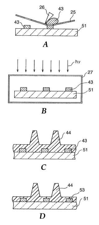
Fig. 3 is sectional views illustrating the manufacturing process of a
substrate for a
PDP according to the present in order. As shown in Fig. 3 (A), a stripe-shaped
electrode
precursor layer 43 is printed in advance in a predetermined pattern on the
surface of the
glass substrate 51. In this example, the screen printing method is used,
therefore, the
photo-curable silver paste 43 as an electrode precursor is extruded-onto the
glass substrate
51 through the opening of a screen printing mask 25. To improve the efficiency
in
extrusion, a squeezer 26 is used.
13
CA 02544935 2006-05-04
WO 2005/052974 PCT/US2004/032801
Next, in order to cure the silver paste after printed, the glass substrate 51
is put into
a curing oven 27 and irradiated with light such as ultraviolet rays (hv) under
a nitrogen gas
atmosphere, as shown in Fig.3 (B). The silver paste is cured and the electrode
precursor
layer 43 is thus formed.
After the electrode precursor layer is formed as described above, a rib
precursor
layer 44 is formed on the glass substrate 51 as shown in Fig.3 (C). First, the
glass substrate
is taken out from the curing oven, and after a forming mold on which a desired
rib pattern
has been formed is aligned in advance so that the rib pattern is formed
between the
electrode patterns, a paste-like photo-curable rib precursor is coated on the
glass substrate
and the forming mold is laminated thereon. Then, the paste-like rib precursor
is cured by
the irradiation of light (for example, ultraviolet rays) that can cause the
rib precursor to
react. After the rib precursor is cured, the used forming mold is removed.
The forming process of the rib precursor layer shown in Fig. 3 (C) can be
preferably carned out by use of the method that is illustrated in order in
Fig. 4. Note that,
the present process can be advantageously carried out by use of the
manufacturing
equipment shown in Figs. 1 to 3 of JP 2001-191345.
First, a glass substrate equipped with a stripe-shaped electrode precursor
layer is
prepared and set on a base of the production apparatus. Then, as shown in Fig.
4 (A), a
flexible forming mold 20 consisting of a supporting body 21 that supports a
shaping layer
22 having a groove pattern on its surface is placed at a predetermined
position on the glass
substrate 51, and the glass substrate 51 and the forming mold 20 is aligned.
As shown, the
electrode precursor layer 43 has already been formed on the surface of the
glass substrate
51. As the forming mold 20 is transparent, it is possible to easily align
itself with the
electrode on the glass substrate 51. To be precise, it is possible to carry
out the alignment
visually or by use of a sensor such as a CCD camera. At this time, if
necessary, it is
possible to make the groove of the forming mold 20 coincide with the distance
between
two neighboring electrodes on the glass substrate by adjusting temperature and
humidity.
This is because the forming mold 20 and the glass substrate 51 extend or
contract
according to the change in temperature and humidity but differ in the
magnitude in
extension or contraction. Therefore, after the alignment between the glass
substrate 51 and
the forming mold 20 is completed, it is necessary to control the temperature
and humidity
so that they are maintained unchanged. This controlling method is particularly
effective in
14
CA 02544935 2006-05-04
WO 2005/052974 PCT/US2004/032801
manufacturing a substrate for a large PDP.
Subsequently, a laminate roll 23 is mounted on one end of the forming mold 20.
Preferably, the laminate roll 23 is a rubber roll. At this time, it is
preferable that one end of
the forming mold 20 is fixed onto the glass substrate 51. This is because the
glass substrate
51 and the forming mold 20 that have already been aligned are prevented from
deviating
from each other.
Next, the other end of the forming mold 20 is lifted up over the laminate roll
23 by
use of a holder (not shown) so that the glass substrate 51 is laid bare. At
this time, be
caxeful not to exert tension on the forming mold 20. This is because to
prevent wrinkles
from occurring in the forming mold 20 and maintain the alignment between the
forming
mold 20 and the glass substrate 51. However, as long as the alignment is
maintained, other
means can be used. In the present method, even if the forming mold 20 is
lifted up as
shown schematically, the exact alignment can be resumed in the following
laminating
process, because the forming mold 20 has elasticity.
Thereafter, a predetermined amount of the rib precursor 44 necessary for
forming
ribs is supplied onto the glass substrate 51. A nozzle-attached paste hopper,
for example,
can be used for supply of the rib precursor. The details of the rib precursor
have been
described above.
Next, a rotary motor (not shown) is driven to move the laminate roll 23 on the
forming mold 20 at a predetermined speed in the direction of the arrow in
Fig.4 (A). As
the laminate roll 23 moves on the forming mold 20 in this manner, a pressure
due to the
self weight of the laminate roll 23 is sequentially applied to the forming
mold 20 from the
one end to the other, thus the rib precursor 44 spreads between the glass
substrate 51 and
the forming mold 20 and the grooves of the forming mold 20 are also filled
therewith. At
this time, the thickness of the rib precursor can be adjusted in a range
between several ~,m
to tens of ~,m by properly controlling the viscosity of the rib precursor or
the diameter,
weight or traveling speed of the laminate roller.
y
According to the illustrated method, even if the groove of the forming mold
captures air herein as an air channel, the captured air can be efficiently
excluded to the
outside or the ambient area of the forming mold when the above-mentioned
pressure is
exerted. As a result, the present method is capable of preventing bubbles from
remaining
even if the filling of the rib precursor is carried out under the atmospheric
pressure. In
CA 02544935 2006-05-04
WO 2005/052974 PCT/US2004/032801
other words, depressurization is not required for the filling of the rib
precursor. Of course,
it is possible to more easily remove the bubbles by means of depressurization.
Subsequently, the rib precursor is cured. When the rib precursor 44 spread on
the
glass substrate 51 is photo-curable, the laminated body of the glass substrate
51 and the
forming mold 20 is put in a light irradiation apparatus (not shown) and the
rib precursor 44
is irradiated with light such as ultraviolet rays for curing via the glass
substrate 51 and the
forming mold 20. Thus, the rib precursor layer 44 as shown in Fig. 4 (C) can
be obtained.
After the electrode precursor layer and the rib precursor layer are
sequentially
formed, as described above, in a state in which these layers are bonded to the
glass
substrate, the glass substrate and the forming mold are taken out from the
light irradiation
apparatus and the forming mold 20 is peeled off and removed as shown in Fig.4
(C).
Because the forming mold 20 used here is excellent also in handling, it is
possible to easily
peel off and remove the forming mold 20 with a small force without destroying
the rib
precursor layer 44 bonded to the glass substrate 51. Of course, huge equipment
is not
required for this peeling and removing work.
Next, the glass substrate on which the electrode precursor layer and the rib
precursor layer have been formed is put in a sintering oven and the two layers
are sintered
simultaneously according to the predetermined sintering schedule. Although the
sintering
temperature can be changed in a wide range, as described above, a range of
approximately
400 to 600°C is normal. When the glass substrate is taken out from the
sintering oven, the
glass substrate 51, equipped with the electrodes 53 and the ribs 54 each
formed with more
or less contraction, is obtained, as shown in Fig.3 (D). The formed product
thus obtained
exactly coincides with the objective substrate for a PDP both in the shape and
in the
dimensions and is free from defects such as a deficiency of barrier rib.
Now, the present invention is described with reference to examples thereof.
Note
that these examples do not restrict the present invention.
Example 1
Preparation of a silver paste for electrode formation:
The following components were mixed carefully to prepare a photo-curable
silver
paste, in which each component was uniformly dispersed:
16
CA 02544935 2006-05-04
WO 2005/052974 PCT/US2004/032801
Silver powder (manufactured by Tanaka Kikinzoku Kogyo K.K.)
65.7 g
Low-melting point lead glass powder (manufactured by Asahi Glass Co.)
2.7 g
Photo-curable oligomer: bisphenol A diglycidyl methacrylate acid adduct
(manufactured
by Kyoeisha Chemical Co., Ltd.)
7.5 g
Photo-curable monomer: triethylene glycol dimethacrylate (manufactured by Wako
Pure
Chemical Industries, Ltd.)
3.0 g
Diluent: l, 3-butanediol (manufactured by Wako Pure Chemical Industries, Ltd.)
10.5 g
Photo-curing initiator: 2-benzoyl 2-dimethoxyamino-1-(4-morpholinophenyl)
butanone-1
(manufactured by Ciba-Gigy)
0.6 g
Preparation of a ceramic paste for rib formation:
The following components were mixed carefully to prepare a photo-curable
ceramic paste, in which each component was uniformly dispersed:
Photo-curable oligomer: bisphenol A diglycidyl methacrylate acid adduct
(manufactured
by Kyoeisha Chemical Co., Ltd.)
21.0 g
Photo-curable monomer: triethylene glycol dimethacrylate (manufactured by Wako
Pure
Chemical Industries, Ltd.)
9.0 g
Diluent: 1, 3-butanediol (manufactured by Wako Pure Chemical Industries, Ltd.)
30.0 g
Photo-curing initiator: bis (2, 4, 6-trimethylbenzoyl)-phenylphosphineoxide)
(manufactured by Ciba Specialty Chemicals K.K., the product name
"IRGACURE819")
17
CA 02544935 2006-05-04
WO 2005/052974 PCT/US2004/032801
0.3 g
Surface active agent: phosphate propoxyalkyl polyol
3.0 g
Inorganic particles: a mixture of lead glass and ceramic particles
(manufactured by Asahi
Glass Co.)
180.0g
Manufacture of a back plate for PDP:
A glass substrate made of soda-lime glass having a thickness of 2.8 mm was
prepared and the photo-curable silver paste prepared as described above was
coated on the
surface of the glass substrate by use of the screen printing method. The
screen printing
mask used in this example had an opening for electrode pattern formation
having a width
of 120 p,m and a pitch of 300 ~,m.
Next, the glass substrate on which the silver paste had been coated was put in
a
closed vessel having a quartz glass window, and the inside of the vessel is
filled with
nitrogen gas and purged of oxygen until the oxygen concentration fell below
0.1 %. The
coating film of silver paste was irradiated for 20 seconds with ultraviolet
rays having a
wavelength of 300 to 400 nm (D-bulb made by FUSION UV Systems, Inc.) through
the
quartz glass window and thus the silver paste was cured. Then, the glass
substrate
equipped with the silver electrode precursor layer was taken out from the
closed vessel.
In order to form ribs by use of the transfer method, a flexible forming mold
designed to form a rib precursor having a rib pitch of 300 p,m, a rib height
of 200 p,m and
a rib top width of 80 p,m was prepared. The forming mold was arranged through
the
positional alignment on the glass substrate equipped with the silver electrode
precursor
layer so that the groove pattern of the forming mold was opposed to the glass
substrate.
Then, the gap between the forming mold and the glass substrate was filled with
the photo-
curable ceramic paste prepared as described above.
After the filling of the ceramic paste was completed, the forming mold was
laminated in such a way that the surface of the glass substrate was covered
therewith. The
grooves of the forming mold were completely filled with the ceramic paste by
carefully
pressing the forming mold by use of the laminate roll.
18
CA 02544935 2006-05-04
WO 2005/052974 PCT/US2004/032801
In this state, both the surfaces of the forming mold and the glass substrate
were
irradiated for 30 seconds with ultraviolet rays having a wavelength of 400 to
450 nm (peak
wavelength: 352 nm) by use of a fluorescent lamp manufactured by Philips Co.
The
quantity of irradiation of ultraviolet rays was 200 to 300 mJlcm2. The ceramic
paste cured
and became a barrier rib precursor layer. Then, the glass substrate together
with the rib
precursor layer thereon was peeled from the forming mold.
The glass substrate equipped with the silver electrode precursor layer and the
rib
precursor layer was put in the sintering oven and sintered at a temperature of
550°C for
one hour. After the sintered glass substrate was taken out from the sintering
oven, the
objective back plate for a PDP with silver electrodes and ribs was obtained.
It was
confirmed that the silver electrodes and ribs were formed simultaneously
without any
damages to the back plate. The electrical resistivity of the silver electrode
was 1 ohm per 1
cm, for both the portion formed on the rib and the portion not formed on the
rib,
respectively, and from this fact it was confirmed that the silver electrode
was conductive.
Moreover, it was confirmed that the electrical resistivity between neighboring
silver
electrodes was infinity and that the silver electrodes were formed properly.
Example 2
A back plate for a PDP was manufactured by repeating the processes described
in
Example 1. In this example, however, the same amount (0.6 g) of bis (2, 4, 6-
trimethylbenzoyl) - phenylphosphineoxide) (manufactured by Ciba Specialty
Chemicals
K.K., the product name "IRGACURES19) was used instead of 2-benzoyl-2-
dimethoxyamino 1-(4-morpholinophenyl) butanone-1 as a photo-curing initiator
in
preparing the photo-curable silver paste. Moreover, for curing, the silver
paste was
irradiated for 20 seconds with ultraviolet rays having a wavelength of 400 to
500 nm (D-
bulb made by FUSION UV Systems, Inc.) through the quartz glass window.
The glass substrate equipped with the silver electrode precursor layer and the
rib
precursor layer was put in a sintering oven and sintered for one hour at a
temperature of
_ 550°C. The sintered glass ubstrate was_taken out from the sintering
oven, and the
objective back plate for a PDP with silver electrodes and ribs was obtained.
It was
confirmed that the silver electrodes and ribs were formed simultaneously
without any
damages to the back plate. The electrical resistivity of the silver electrode
was 1 ohm per 1
19
CA 02544935 2006-05-04
WO 2005/052974 PCT/US2004/032801
cm, for both the portion formed on the rib and the portion not formed on the
rib,
respectively, and from this fact it was confirmed that the silver electrode
was conductive.
Moreover, it was confirmed that the electrical resistivity between neighboring
silver
electrodes was infinity and that the silver electrodes were formed properly.
Comparison example 1
A back plate for a PDP was manufactured by repeating the processes described
in
Example 1. In this example, however, for comparison, the back plate for a PDP
was
manufactured according to the following procedure by use of the photo-curable
silver
paste and the photo-curable.ceramic paste prepared in Example 1.
A glass substrate made of soda-lime glass having a thickness of 2.8 mm was
prepared and the photo-curable silver paste was coated on the surface of the
glass substrate
by use of the screen printing method. The screen printing mask used in this
example had
an opening for electrode pattern formation having a width of 120 ~.m and a
pitch of 300
Vim.
Next, the glass substrate on which the silver paste had been coated was put in
a
closed vessel having a quartz glass window. Under an ambient atmosphere, the
coating
film of silver paste was irradiated for 20 seconds with ultraviolet rays
having a wavelength
of 300 to 400 nm (D-bulb made by FUSION UV Systems, Inc.) through the quartz
glass
window and thus the silver paste was cured. The glass substrate equipped with
the silver
electrode precursor layer in which the silver paste had not cured well was
taken out from
the closed vessel.
In order to form ribs by use of the transfer method, a flexible forming mold
designed to form a rib precursor having a rib pitch of 300 ~,m, a rib height
of 200 ~,m and
a rib top width of 80 p,m was prepared. The forming mold was arranged through
the
positional alignment on the glass substrate equipped with the silver electrode
precursor
layer so that the groove pattern of the forming mold was opposed to the glass
substrate.
Then, the gap between. the forming mold and the glass substrate was filled
with the photo-
curable ceramic paste. - - -- -
After the filling of the ceramic paste was completed, the forming mold was
laminated in such a way that the surface of the glass substrate was covered
therewith. The
grooves of the forming mold were completed filled with the ceramic paste by
carefully
CA 02544935 2006-05-04
WO 2005/052974 PCT/US2004/032801
pressing the forming mold by use of the laminate roll. At this moment,
however, the silver
paste that had not cured well was mixed with the ceramic paste and the
electrode pattern
was destroyed. After the destruction of the electrode pattern was recognized,
further
photo-curing process for curing the ceramic paste was omitted. As a result, it
was
impossible to obtain a back plate for a PDP equipped with silver electrodes
and ribs in this
example.
21