Note: Descriptions are shown in the official language in which they were submitted.
CA 02545163 2006-05-08
WO 2005/048364 PCT/US2004/038028
LIGHT EMITTING DEVICES WITH SELF ALIGNED OHMIC CONTACT AND
METHODS OF FABRICATING SAME
RELATED APPLICATION AND CLAIM OF PRIORITY
The present application is related to and claims priority from United
States Provisional Patent Application Serial No. 60/519,425, filed November
12, 2004 and entitled "LED WITH SELF ALIGNED OHMIC CONTACT," the
disclosure of which is incorporated herein as if set forth in its entirety.
BACKGROUND OF THE INVENTION
1. Field of the Invention
The present invention relates to semiconductor devices, and more
particularly to light emitting devices having an ohmic contact formed on an
epitaxial layer.
2. Description of the Related Art
Light emitting diodes (or LEDs) are well known solid state electronic
devices capable of generating light upon application of a sufficient voltage.
Light emitting diodes generally comprise a p-n junction formed in an epitaxial
layer deposited on a substrate such as sapphire, silicon, silicon carbide,
gallium arsenide and the like. The wavelength distribution of the light
generated by the LED depends on the material from which the p-n junction is
fabricated and the structure of the thin epitaxial layers that comprise the
active
region of the device.
Commonly, an LED includes an n-type substrate, an n-type epitaxial
region formed on the substrate and a p-type epitaxial region formed on the n-
type epitaxial region. In order to facilitate the application of a voltage to
the
device, an anode ohmic contact is formed on a p-type region of the device
(typically, an exposed p-type epitaxial layer) and a cathode ohmic contact
must be formed on an n-type region of the device (such as the substrate or an
exposed n-type epitaxial layer).
1
CA 02545163 2006-05-08
WO 2005/048364 PCT/US2004/038028
Because it is difficult to make highly conductive p-type Group III-nitride,
materials (such as GaN, AIGaN, InGaN, AIInGaN, and AIInN), lack of current
spreading in the p-type layer may be a limiting factor in the performance of
LEDs formed from such materials. Accordingly, it is desirable to form an
ohmic contact over as much of the surface area of the exposed p-type layer
as possible in order to induce current to pass through as much of the active
region of the device as possible. Moreover, patterning an ohmic contact
conventionally requires at least one photolithography step. Photolithography
may be an expensive and time consuming step in the semiconductor device
fabrication process. It is desirable to reduce the number of photolithography
steps required for device fabrication.
SUMMARY OF THE INVENTION
In some embodiments, a light emitting diode includes a substrate and
an epitaxial region formed on the substrate. The epitaxial region includes an
n-type epitaxial region formed on the substrate and a p-type epitaxial region
formed on the n-type epitaxial region. At least a portion of the epitaxial
region
including surface portions of the p-type epitaxial region are formed in the
shape of a mesa. An ohmic contact is formed on exposed portions of the p-
type epitaxial layer. The ohmic~contact is self aligned to the mesa and to the
p-type epitaxial layer_ The sidewalls of the mesa may be semi-insulating for
protection of the p-n junction to discourage degradation and failure of the
device.
Method embodiments of the invention include forming an epitaxial
region on a substrate including an n-type region and a p-type region; forming
an ohmic contact on exposed portions of the p-type epitaxial layer; applying
an etch mask to portions of the ohmic contact; etching through exposed
portions of the ohmic contact; with the mask in place, continuing etching
through exposed portions of the epitaxial region to form a mesa; and
removing the etch mask. The sidewalls of the mesa may be implanted with
ions in a manner that causes the surface of the sidewalls to become semi-
insulating.
2
CA 02545163 2006-05-08
WO 2005/048364 PCT/US2004/038028
Further embodiments of the present invention provide light emitting
devices that include a substrate, an n-type epitaxial region on the substrate
and a p-type epitaxial region on the n-type epitaxial region. At least a
portion
of the p-type epitaxial region comprises a mesa with respect to the substrate.
An ohmic contact is provided on an exposed portion of the p-type epitaxial
layer. The ohrnic contact is self aligned to a sidewall of the mesa and to the
p-type epitaxial layer such that a sidewall of the ohmic contact is
substantially
aligned with a sidewall of the mesa and to the p-type epitaxial layer.
In some embodiments of the present invention, a sidewall of the mesa
is configured such that a portion of the substrate extends beyond the sidewall
of the mesa. A portion of the p-type epitaxial region and/or the n-type
epitaxial region of the mesa adjacent the sidewall of the mesa may be semi-
insulating.
In further embodiments of the present invention, the mesa has a
sidewall extending through the p-type epitaxial region. The mesa may have a
sidewall extending through the p-type epitaxial region and into the n-type
epitaxial region. The mesa may also have a sidewall extending through the p-
type epitaxial region and the n-type epitaxial region. The mesa may have a
sidewall extending to the substrate.
In particular embodiments, the light emitting device is a light emitting
diode. The light emitting device could also be a laser diode.
In further embodiments of the present invention, the p-type epitaxial
region comprises a Group III-nitride epitaxial layer and the n-type epitaxial
region comprises a Group III-nitride epitaxial Payer. The substrate may be a
SiC substrate or a sapphire substrate. The ohmic contact include platinum.
In still further embodiments of the present invention, methods of
fabricating a light emitting device include forming an n-type epitaxial layer
on
a substrate, forming a p-type epitaxial layer on the n-type epitaxial layer,
forming an ohmic contact layer on exposed portions of the p-type epitaxial
layer, etching through exposed portions of the ohmic contact layer to provide
a patterned ohmic contact and etching into the p-type epitaxial layer using
the
patterned ohmic contact as a mask to form a mesa.
Further embodiments of the present invention include applying an etch
mask to portions of the ohmic contact layer. In such embodiments, etching
3
CA 02545163 2006-05-08
WO 2005/048364 PCT/US2004/038028
through exposed portions of the ohmic contact layer includes etching through
the ohmic contact layer using the etch mask. The etch mask may also be
removed.
In additional embodiments of the present invention, etching into the p
type epitaxial layer includes etching into the p-type epitaxial layer using
the
etch mask on the ohmic contact layer as a mask and removing the etch mask
is preceded by etching into the p-type epitaxial layer.
In some embodiments of the present invention, etching into the p-type
epitaxial layer includes etching into the p-type epitaxial layer using the
etch
mask such that a sidewall of the mesa is configured such that a portion of the
substrate extends beyond the sidewall of the mesa.
Additional embodiments of the present invention include ion implanting
the sidewall of the mesa such that a portion of the p-type epitaxial layer of
the
mesa adjacent the sidewall of the mesa is made semi-insulating.
In yet other embodiments of the present invention, etching into the p-
type epitaxial layer includes etching through the p-type epitaxial layer such
that a sidewalls extends through the p-type epitaxial layer. Etching into the
p-
type epitaxial layer may also include etching through the p-type epitaxial
layer
and into the n-type epitaxial layer such that a sidewall of the mesa extends
through the p-type epitaxial layer and into the n-type epitaxial layer.
Etching
into the p-type epitaxial layer could also include etching through the p-type
epitaxial layer and the n-type epitaxial layer such that a sidewall of the
mesa
extends through the p-type epitaxial layer and the n-type epitaxial layer.
Etching into the p-type epitaxial layer could include etching through the p-
type
epitaxial layer and the n-type epitaxial layer such that a sidewall of the
mesa
extends through the p-type epitaxial layer and the n-type epitaxial layer and
to
the substrate.
BRIEF DESCRIPTION OF THE DRAWINGS
Figures 1A-1F illustrate conventional methods of forming an ohmic contact.
Figures 2A-C illustrate methods of forming an ohmic contact according to
embodiments of the invention.
Figure 3 is a cross-sectional drawing illustrating implantation of ions into
the
sidewalls of a mesa.
4
CA 02545163 2006-05-08
WO 2005/048364 PCT/US2004/038028
DETAILED DESCRIPTION
The present invention now will be described more fully hereinafter with
reference to the accompanying drawings, in which embodiments of the
invention are shown. This invention should not be construed as limited to the
embodiments set forth herein; rather, these embodiments are provided so that
this disclosure will be thorough and complete, and will fully convey the scope
of the invention to those skilled in the art. Like numbers refer to like
elements
throughout. Furthermore, the various layers and regions illustrated in the
figures are illustrated schematically. As will also be appreciated by those of
skill in the art, while the present invention is described with respect to
semiconductor wafers and diced chips, such chips may be diced into arbitrary
sizes. Accordingly, the present invention is not limited to the relative size
and
spacing illustrated in the accompanying figures. In addition, certain features
of the drawings are illustrated in exaggerated dimensions for clarity of
drawing
and ease of explanation.
The terminology used herein is for the purpose of describing particular
embodiments only and is not intended to be limiting of the invention. As used
herein, the singular forms "a", "an" and "the" are intended to include the
plural
forms as well, unless the context clearly indicates otherwise. It will be
further
understood that the terms "comprises" andlor "comprising," when used in this
specification, specify the presence of stated features, integers, steps,
operations, elements, andlor components, but do not preclude the presence
or addition of one or more other features, integers, steps, operations,
elements, components, andlor groups thereof.
It will be understood that when an element such as a layer, region or
substrate is referred to as being "on" or extending "onto" another element, it
can be directly on or extend directly onto the other element or intervening
elements may also be present. In contrast, when an element is referred to as
being "directly on" or extending "directly onto" another element, there are no
intervening elements present. It will also be understood that when an element
is referred to as being "connected" or "coupled" to another element, it can be
directly connected or coupled to the other element or intervening elements
may be present. In contrast, when an element is referred to as being "directly
5
CA 02545163 2006-05-08
WO 2005/048364 PCT/US2004/038028
connected" or "directly coupled" to another element, there are no intervening
elements present. Like numbers refer to like elements throughout the
specification.
It will be understood that, although the terms first, second, etc. may be
used herein to describe various elements, components, regions, layers and/or
sections, these elements, components, regions, layers and/or sections should
not be limited by these terms. These terms are only used to distinguish one
element, component, region, layer or section from another region, layer or
section. Thus, a first element, component, region, layer or section discussed
below could be termed a second element, component, region, layer or section
without departing from the teachings of the present invention.
Furthermore, relative terms, such as "lower" or "bottom" and "upper" or
"top," may be used herein to describe one element's relationship to another
elements as illustrated in the Figures. It will be understood that relative
terms
are intended to encompass different orientations of the device in addition to
the orientation depicted in the Figures. For example, if the device in the
Figures is turned over, elements described as being on the "lower" side of
other elements would then be oriented on "upper" sides of the other elements.
The exemplary term "lower", can therefore, encompasses both an orientation
of "lower" and "upper," depending of the particular orientation of the figure.
Similarly, if the device in one of the figures is turned over, elements
described
as "below" or "beneath" other elements would then be oriented "above" the
other elements. The exemplary terms "below" or "beneath" can, therefore,
encompass both an orientation of above and below.
Embodiments of the present invention are described herein with
reference to cross-section illustrations that are schematic illustrations of
idealized embodiments of the present invention. As such, variations from the
shapes of the illustrations as a result, for example, of manufacturing
techniques and/or tolerances, are to be expected. Thus, embodiments of the
present invention should not be construed as limited to the particular shapes
of regions illustrated herein but are to include deviations in shapes that
result,
for example, from manufacturing. For example, an etched region illustrated or
described as a rectangle will, typically, have rounded or curved features.
Thus, the regions illustrated in the figures are schematic in nature and their
6
CA 02545163 2006-05-08
WO 2005/048364 PCT/US2004/038028
shapes are not intended to illustrate the precise shape of a region of a
device
and are not intended to limit the scope of the present invention.
Unless otherwise defined, all terms (including technical and scientific
terms) used herein have the same meaning as commonly understood by one
of ordinary skill in the art to which this invention belongs. It will be
further
understood that terms, such as those defined in commonly used dictionaries,
should be interpreted as having a meaning that is consistent with their
meaning in the context of the relevant art and will not be interpreted in an
idealized or overly formal sense unless expressly so defined herein.
It will also be appreciated by those of skill in the art that references to,a
structure or feature that is disposed "adjacent" another feature may have
portions that overlap or underlie the adjacent feature.
Although various embodiments of LEDs disclosed herein include a
substrate, it will be understood by those skilled in the art that the
crystalline
epitaxial growth substrate on which the epitaxial layers comprising an LED are
grown may be removed, and the freestanding epitaxial layers may be
mounted on a substitute carrier substrate or submount which may have better
thermal, electrical, structural and/or optical characteristics than the
original
substrate. The invention described herein is not limited to structures having
crystalline epitaxial growth substrates and may be utilized in connection with
structures in which the epitaxial layers have been removed from their original
growth substrates and bonded to substitute carrier substrates.
Embodiments of the invention now will be described, generally with
reference to gallium nitride-based light emitting diodes on silicon carbide-
based substrates. However, it will be understood by those having skill in the
art that many embodiments of the invention may be employed with many
different combinations of substrate and epitaxial layers. For example,
combinations can include AIGaInP diodes on GaP substrates; InGaAs diodes
on GaAs substrates; AIGaAs diodes on GaAs substrates; SiC diode on SiC
or sapphire (AI203) substrate; and/or a nitride-based diodes on gallium
nitride, silicon carbide, aluminum nitride, sapphire, zinc oxide and/or other
substrates.
GaN-based light emitting diodes (LEDs) typically comprise an insulating
or semiconducting substrate such as SiC or sapphire on which a plurality of
7
CA 02545163 2006-05-08
WO 2005/048364 PCT/US2004/038028
GaN-based epitaxial layers are deposited. The epitaxial layers comprise an
active region having a p-n junction that emits light when energized.
Figure 1A schematically illustrates a precursor structure for an LED
device having an n-type SiC substrate 10, an active region comprising an n-
GaN-based layer 14 and a p-GaN-based layer 16 grown on the substrate.
An ohmic contact 18 is formed on the p-GaN layer 16. Ohmic contact layer
18 may comprise a thin (< 100 A) layer of platinum deposited by evaporation.
Formation of ohmic contacts on gallium nitride layers is described for example
in U.S. Patent Application Publication Number 2003/0025121 entitled "Robust
Group III Light Emitting Diode for High Reliability in Standard Packaging
Applications" which is assigned to the assignee of the present invention and
which is incorporated herein by reference as if fully set forth herein.
In order to pattern the ohmic contact, an etch mask 15 may be formed on
the ohmic contact layer 18 as illustrated in Figure 1 B. Etch mask 15 may
comprise photoresist or any suitable material which resists etching by a
chlorine-based dry etch. In one such process, after formation of ohmic
contact 18, a layer of photoresist is applied to the top surface of the
device.
The photoresist is selectively exposed using a mask and exposed portions of
the photoresist are developed out (i.e. removed) to leave a portion of the
photoresist on the upper surface of the ohmic contact layer 18 to act as an
etch mask.
Next, as illustrated in Figure 1C, exposed portions of the ohmic contact
layer are etched away using a chlorine-based dry etch. Dry etching using a
chlorine-based etchant is described in U.S. Patent No. 5,631,190 which is
assigned to the assignee of the present invention and is incorporated herein
by reference.
After etching for a sufficient time to remove exposed portions of the
ohmic contact, the etch mask 15 is optionally removed and a second etch
mask 17 is formed over ohmic contact 18 and also over exposed portions of
p-type layer 16. Due to the width tolerance of the photolithographic process,
etch mask 17 may overlap the ohmic contact by about 1-2 arm or more. As
illustrated in Figure 1 E, the p-type layer 16 and n-type layer 14 are then
etched (using a chlorine-based dry etch in some embodiments) to reveal a
portion of the surface of substrate 10. The etch mask 17 is then removed as
8
CA 02545163 2006-05-08
WO 2005/048364 PCT/US2004/038028
illustrated in Figure 1 F. If the etch mask is a photoresist, it may be
removed
through immersion in a solvent such as acetone or a stripper such as N-
methylpyrolidinone.
A bond pad (not shown) may be formed on the ohmic contact 18 and a
passivation layer (not shown) may be formed over the upper surface of the
device. The passivation layer may comprise a dielectric material such silicon
nitride or silicon dioxide and may be deposited using a conventional method
such as PECVD deposition or sputtering. Methods of forming passivation
layers are described in detail in the aforementioned U.S. Patent Application
Publication No. 2003/0025121.
Photolithography steps such as those described above are expensive
and time consuming, since they require multiple steps and precise alignment
of a mask to a wafer.
Embodiments of the invention which use a reduced number of
photolithography steps are illustrated in Figures 2A-2C. In these
embodiments, an etch mask 19 is formed on portions of the surface of ohmic
contact layer 18 as illustrated in Figure 2A. Next, as shown in Figure 2B, the
ohmic contact layer 18 is etched along with p-type epitaxial layer 16 and, in
some embodiments, the n-type epitaxial layer 14, to expose portions of the
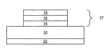
surface of substrate 10 and form mesa 27. Thus, a mesa is formed having a
sidewall that extends into the p-type epitaxial layer 16. In some
embodiments, the etch is performed until the sidewall of the mesa extends
through the p-type epitaxial layer 16 and, in some embodiments, into the n-
type epitaxial layer 14. In further embodiments, the etch is performed until
the
sidewall of the mesa extends through the p-type epitaxial layer 16 and
through the n-type epitaxial layer 14. In some embodiments, the etch is
performed until the sidewall extends to and/or into the substrate 10. In some
embodiments, the etch extends into but not through the substrate, thus
maintaining a mesa with respect to the substrate.
In some embodiments, etching is performed using a chlorine-based dry
etch as described above for a sufficient time to remove both the exposed
ohmic contact metal 18 as well as the Group III-nitride based epitaxial
layers.
As shown in Figure 2C, the etch mask is then removed.
9
CA 02545163 2006-05-08
WO 2005/048364 PCT/US2004/038028
Although substrate 10 is SiC in the illustrated embodiment, substrate
may comprise any other suitable substrate material such as sapphire,
silicon, gallium arsenide and the like.
A blanket passivation layer (not shown) may be formed over the
5 exposed upper surfaces of the device. The passivation layer may comprise a
dielectric material such silicon nitride or silicon dioxide and may be applied
by
known methods such as PECVD or sputter deposition.
In order to protect the p-n junction, prior to removal of the mesa etch
mask 19, the exposed surfaces of the mesa may be implanted with ions to
10 render the surfaces semi-insulating. Methods of ion implantation are
disclosed in U.S. Patent Application Serial No. (Attorney Docket
No. 5000.270A) entitled "Led Fabrication Via Ion Implant Isolation," Slater et
al. inventors, filed concurrently herewith, which is incorporated herein by
reference as if fully set forth fully herein.
In preferred methods of ion implantation, the wafer is tilted and ions are
implanted into the sidewalls of the mesa. Since the wafer is tilted during
implantation, the implanted ions strike the sides of the mesa at a relatively
steep angle. Since the entire sidewall is implanted at once, multiple implants
are not required. Also, the dose and depth of the implant may be reduced.
As a result, the volume of the implanted region is reduced, thereby reducing
light absorption within the implanted region. The implant depth may be 0.1-
0.2 pm. The wafer may be rotated during the implant for uniformity. In one
embodiment, the wafer is rotated 8 times during implantation. The implant
dose may be 2x10'3cm-2 N+ at 60keV at a 60 degree angle. Rotating the
wafer reduces the implant dose by a factor of 4 for square mesas. Thus, an
implant dose of 2x'10'3cm-2 actually results in a dose of 5x10~2cm-2 per side
for a four-sided mesa structure.
Turning to Figure 3, after growth of the epitaxial layers on the substrate
and mesa formation (for simplicity, only one mesa 27 is illustrated in Figure
3.)
the substrate 10 is mounted on a tiltable, rotatable wafer carrier (not shown)
and placed in an ion implanter. The wafer carrier is tilted to make the
sidewalls 27A of the mesas 27 as close to horizontal as possible (i.e. as
close
as possible to perpendicular to the implant direction). In one embodiment, the
wafer carrier is tilted by at least 45° and preferably by 60°
such that the
CA 02545163 2006-05-08
WO 2005/048364 PCT/US2004/038028
implant direction is less about 25° from a direction normal to the mesa
sidewall 27A. In the illustrated embodiment, the mesa makes an angle of
about 105° with the substrate, resulting in an implant angle of about
15° from
normal. Ions 112 are then implanted into the mesa sidewall to form an
implanted region 114 which extends approximately 0.1-0.2 pm into the mesa
sidewall 27A. As discussed above, the wafer carrier may be rotated one time
or a plurality of times during implantation for uniformity. By implanting the
sidewalls 27A of the mesas 27, only a single implant may be required to
effectively render regions of the sidewalls 27A semi-insulating.
While embodiments of the present invention have been described with
reference to light emitting diodes (LEDs), some embodiments of the present
invention may be utilized with other light emitting devices, such a laser
diodes.
Accordingly, the term light emitting device is used herein to refer to devices
that emit light in the visible or non-visible spectrum and the light may be
coherent or incoherent.
Furthermore, while embodiments of the present invention have been
described with reference to the etch mask 19 being used for a single etch
step, other embodiments of the present invention may use multiple etch steps
with either the etch mask 19 or the patterned ohmic contact layer 18 as a
mask. Such may be case, for example, if a second etch step is used where
the etchant utilized has etch selectivity with respect to the ohmic contact
material and the underlying epitaxial layers. In such a case a self aligned
structure that provides a mesa with a sidewall that is substantially aligned
(i.e.
not differing by substantially more than results from differences in lateral
etch
rate) with the sidewall of the ohmic contact may be provided with only a
single
application and patterning of the etch mask 19.
In the drawings and specification, there have been disclosed
embodiments of the invention and, although specific terms are employed, they
are used in a generic and descriptive sense only and not for purposes of
limitation, the scope of the invention being set forth in the following
claims.
11