Note: Descriptions are shown in the official language in which they were submitted.
CA 02545241 2006-05-08
WO 2005/050704 PCT/US2004/037845
MICROFLUID EJECTION DEVICE HAVING
EFFICIENT LOGIC AND DRIVER CIRCUITRY
FIELD OF THE INVENTION
The invention relates to microfluid ejection devices and in particular to
ejection heads for ejection devices containing efficient logic and driver
circuitry.
BACKGROUND OF THE INVENTION
Microfluid ejection devices such as ink jet printers continue to experience
wide acceptance as economical replacements for laser printers. Such ink jet
printers
are typically more versatile than laser printers for some applications. As the
capabilities of ink jet printers are increased to provide higher quality
images at
increased printing rates, ejection heads, which are the primary printing
components of
to ink jet printers, continue to evolve and become more complex. As the
complexity of
the ejection heads increases, so does the cost for producing ejection heads.
Nevertheless, there continues to be a need for microfluid ejection devices
having
enhanced capabilities including increased quality and higher throughput rates.
Competitive pressure on print quality and price promote a continued need to
produce
ejection heads with enhanced capabilities in a more economical manner.
SUMMARY OF THE INVENTION
With regard to the foregoing and other objects and advantages there is
provided semiconductor substrate for a microfluid ejection head. The substrate
2o includes a plurality of fluid ejection actuators disposed on the substrate.
A plurality
of driver transistors are disposed on the substrate for driving the plurality
of fluid
ejection actuators. Each of the driver transistors have an active area ranging
from
about 1000 to less than about 15,000 p,m2. A plurality of logic circuits
including at
least one logic transistor are coupled to the driver transistors. The driver
and logic
2s transistors are provided by a high density array of MOS transistors wherein
at least
the logic transistors have a gate length of from about 0.1 to less than about
3 microns.
1
CA 02545241 2006-05-08
WO 2005/050704 PCT/US2004/037845
In another embodiment there is provided a microfluid ejection cartridge for a
microfluid ejection device. The cartridge body has a fluid supply source and
an
ejection head attached to the cartridge body in fluid communication with the
fluid
supply source. The ejection head includes a semiconductor substrate having a
plurality of fluid ejection actuators disposed on the substrate. A plurality
of driver
transistors disposed on the substrate for driving the plurality of fluid
ejection
actuators. Each of the driver transistors have an active area width ranging
from about
100 to less than about 400 microns. A plurality of logic circuits including at
least one
logic transistor are operatively coupled to the driver transistors. The driver
and logic
to transistors comprise a high density array of MOS transistors wherein at
least the logic
transistor has a gate length of from about 0.1 to less than about 3 microns. A
nozzle
plate is attached to the semiconductor substrate for ejecting fluid therefrom
upon
activation of the fluid ejection actuators.
In yet another embodiment there is provided a semiconductor substrate for an
ink jet printhead. The substrate includes a plurality of heater resistors
disposed on the
substrate. The heater resistors have a protective layer of diamond like carbon
with a
thickness ranging from about 1000 to about 3000 Angstroms. A plurality of
driver
transistors are disposed on the substrate for driving the plurality of fluid
ejection
actuators. A plurality of logic circuits including at least one logic
transistor are
coupled to the driver transistors. The driver and logic transistors provide a
high
density array of MOS transistors wherein at least the logic transistors have a
gate
length of from about 0.1 to less than about 3 microns.
An advantage of the invention is that it provides microfluid ejection heads
for
microfluid ejection devices that require substantially less substrate area yet
provide
increased functionality. The semiconductor substrates may be used for a wide
variety
of applications including ink jet printheads, microfluid cooling devices,
delivery of
controlled amounts of pharmaceutical preparations, and the like. In ink jet
printer
applications, the substrates of the invention can significantly reduce the
manufacturing and raw material costs of the printheads incorporating the
ejection
3o heads.
2
CA 02545241 2006-05-08
WO 2005/050704 PCT/US2004/037845
BRIEF DESCRIPTION OF THE DRAWINGS
Further advantages of the invention will become apparent by reference to the
detailed description of preferred embodiments when considered in conjunction
with
the following drawings illustrating one or more non-limiting aspects of the
invention,
s wherein like reference characters designate like or similar elements
throughout the
several drawings as follows:
Fig. 1 is a micro-fluid ejection device cartridge, not to scale, containing a
microfluid ejection head according to the invention;
Fig. 2 is a perspective view of a preferred microfluid ejection device
according
l0 to the invention;
Fig. 3 is a cross-sectional view, not to scale of a portion of a microfluid
ejection head according to the invention;
Fig. 4 is a schematic drawing of a logic circuit according to the invention;
Figs. 5 is a schematic drawing of an inverter for a logic circuit according to
the
1 s invention;
Fig. 6 is a cross-sectional view, not to scale, of a portion of logic circuit
transistors according to the invention;
Figs 7 and 8 are cross-sectional views, not to scale of portions of driver
transistors according to the invention;
20 Fig. 9 is a plan view, not to scale, of a portion of a driver transistor
according
to the invention;
Fig. 10 is a plan view not to scale of a typical layout on a substrate for a
microfluid ejection head according to the invention; i
Fig. 11 is a plan view, not to scale of a portion of an active area of a
25 microfluid ejection head according to the invention; and
Fig. 12 is a partial schematic drawing of a logic diagram for a microfluid
ejection device according to the invention.
DETAILED DESCRIPTION OF THE INVENTION
3o With reference to Fig. 1, a fluid cartridge 10 for a microfluid ejection
device is
illustrated. The cartridge 10 includes a cartridge body 12 for supplying a
fluid to a
3
CA 02545241 2006-05-08
WO 2005/050704 PCT/US2004/037845
fluid ejection head 14. The fluid may be contained in a storage area in the
cartridge
body 12 or may be supplied from a remote source to the cartridge body.
The fluid ejection head 14 includes a semiconductor substrate 16 and a nozzle
plate 18 containing nozzle holes 20. It is preferred that the cartridge be
removably
attached to a micro-fluid ejection device such as an ink jet printer 22 (Fig.
2).
Accordingly, electrical contacts 24 are provided on a flexible circuit 26 for
electrical
connection to the microfluid ejection device. The flexible circuit 26 includes
electrical traces 28 that are connected to the substrate 16 of the fluid
ejection head 14.
An enlarged view, not to scale, of a portion of the fluid ejection head 14 is
1o illustrated in Fig. 3. In this case, the fluid ejection head 14 contains a
thermal heating
element 30 as a fluid ejection actuator for heating the fluid in a fluid
chamber 32
formed in the nozzle plate 18 between the substrate 16 and a nozzle hole 20.
However, the invention is not limited to a fluid ej ection head 14 containing
a thermal
heating element 30. In the case of thermal heating elements 30, the heating
elements
are heater resistors preferably having a protective layer comprising diamond
like
carbon with a thickness ranging from about 1000 to about 3000 Angstroms. Other
fluid ejection actuators, such as piezoelectric devices' may also be used to
provide a
fluid ej ection head according to the invention.
Fluid is provided to the fluid chamber 32 through an opening or slot 34 in the
substrate 16 and through a fluid channel 36 connecting the slot 34 with the
fluid
chamber 32. The nozzle plate 18 is preferably adhesively attached to the
substrate 16
as by adhesive layer 36. As depicted in Fig. 3, the flow features including
the fluid
chamber 32 and fluid channel 36 are formed in the nozzle plate 18. However,
the
flow features may be provided in a separate thick film layer and wherein a
nozzle
plate containing only nozzle holes is attached to the thick film layer. In a
particularly
preferred embodiment, the fluid ejection head 14 is a thermal or piezoelectric
ink jet
printhead. However, the invention is not intended to be limited to ink jet
printheads
as other fluids may be ejected with a microfluid ejection device according to
the
invention.
3o Referring again to Fig. 2, the fluid ejection device is preferably an ink
jet
printer 22. The printer 22 includes a carriage 40 for holding one or more
cartridges
4
CA 02545241 2006-05-08
WO 2005/050704 PCT/US2004/037845
and for moving the cartridges 10 over a media 42 such as paper depositing a
fluid
from the cartridges 10 on the media 42. As set forth above, the contacts 24 on
the
cartridge mate with contacts on the carriage 40 for providing electrical
connection
between the printer 22 and the cartridge 10. Microcontrollers in the printer
22 control
5 the movement of the carriage 40 across the media 42 and convert analog
and/or digital
inputs from an external device such as a computer for controlling the
operation of the
printer 22. Ejection of fluid from the fluid ejection head 14 is controlled by
a logic
circuit 44 on the fluid ejection head 14 in conjunction with the controller in
the printer
22.
1o Figs. 4 and 5, illustrate a preferred logic circuit 44 for a fluid ejection
head 14.
The logic circuit 44 includes a NAND gate 46 with inputs 48 from the
microfluid
ejection device or printer 22 and has an output to an inverter 50. A preferred
inverter
50 is CMOS logic circuit illustrated in Fig. 5 and includes a NMOS transistor
52 in a
P-type substrate and an adjacent PMOS transistor 54 provided by an NWELL in a
P-
type substrate. The output of the inverter 50 is tied to a gate 56 of a driver
transistor
58 that drives the fluid actuator, in this case a thermal heating element 30.
There is at
least one driver transistor 58 adjacent each heater element 30. The heater
element 30
is preferably a resistor having a resistance ranging from about 70 to about
150 ohms
or more, more preferably from about 100 to about 120 ohms.
2o A cross-sectional view, not to scale of an inverter 50 as described above
is
illustrated in Fig. 6. As set forth above, the inverter 50 includes an NMOS
transistor
52 and a PMOS transistor 54. Each of the transistors 52 and 54 preferably have
gates
60 and 62 that have gate lengths ranging from about 0.1 to less than about 3
microns,
most preferably from about 0.1 to about 1.5 microns. Likewise the channels in
the
substrate 64 or NWELL 66 preferably have channel length ranging from about 0.1
to
less than about 3 microns. By providing smaller gate and channel length, a
higher
density of transistors 52 and 54 may be provided for an area of a substrate
containing
the logic circuit 44. Other features of the transistors 52 and 54 are
conventional and
the inverter 50 is produced by conventional semiconductor processing
techniques.
3o Cross-sectional views, not to scale of preferred driver transistors 68 and
70 are
illustrated in Figs. 7 and 8. Fig. 9 is a simplified plan view of driver
transistor 68.
5
CA 02545241 2006-05-08
WO 2005/050704 PCT/US2004/037845
Fig. 7 is a driver transistor 68 having a lightly doped drain region 72,
whereas driver
transistor 70 contains both a lightly doped source region 74 and a lightly
doped drain
region 76. It is also preferred that the driver transistors 68 and 70 include
gates 78
and 80 having gate lengths Lo ranging from about 0.1 to less than about 3
microns
and preferably from about 0.1 to about 1.5 microns and channels having channel
lengths LC (Fig. 9) ranging from about 0.1 to less than about 3 microns. The
gate
length LG of the driver transistors 68 and 70 enables driver transistors
having lower
resistance. Typically the resistance of the driver transistors 68 and 70 is
less than
10% of a total resistance provided in the circuit by the heater resistors 30,
logic circuit
1o 44, driver transistor 68 or 70, and associated connective circuitry. Such
driver
transistors 68 and 70 are preferably operated at a voltage of greater than 8
volts,
preferably from about 8 to about 12 volts.
The driver transistor 68 or 70 includes a substrate 82 which is preferably a P
type silicon substrate. Areas 84 and 86 are N-doped source and drain regions
for
transistors~68 and 70. Area 88 is a P-doped region that provides zero
potential for the
transistor source contacts 90 and 92. Other features of the driver transistors
68 and
70 are conventional and the transistors 68 and 70 are made by conventional
semiconductor processing techniques. It is preferred that the driver
transistor 68 or 70
have an on resistance of less than about 20 ohms, preferably from about 1 to
less than
about 20 ohms.
A plan view, not to scale of a fluid ejection head 14 is shown in Fig. 10. The
fluid ejection head 14 includes a semiconductor substrate 16 and a nozzle
plate 18
attached to the substrate 16. A layout of device areas of the semiconductor
substrate
16 is shown providing preferred locations for logic circuitry 44, driver
transistors 58,
and heater resistors 30. As shown in Fig. 10, the substrate 16 includes a
single slot 34
for providing fluid such as ink to the heater resistors 30 that are disposed
on both
sides of the slot 34. However, the invention is not limited to a substrate 16
having a
single slot 34 or to fluid ejection actuators such as heater resistors 30
disposed on both
sides of the slot 34. Other substrates according to the invention may include
multiple
3o slots with fluid ejection actuators disposed on one or both sides of the
slots. The
substrate may also include no slots 34, whereby fluid flows around the edges
of the
6
CA 02545241 2006-05-08
WO 2005/050704 PCT/US2004/037845
substrate 16 to the actuators. Rather than a single slot 34, the substrate 16
may
include multiples or openings, one each for one or more actuator devices. The
nozzle
plate 18, preferably made of an ink resistant material such as polyimide is
attached to
the substrate 16.
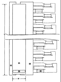
An active area 94 required for the driver transistors 58 is illustrated in
detail in
a plan view of the active area 94 in Fig. 11. This figure represents a portion
of a
typical heater array and active area. The active area 94 of the substrate 16
preferably
has a width dimension W ranging from about 100 to about 400 microns and an
overall
length dimension D ranging from about 6,300 microns to about 26,000 microns.
The
to driver transistors 58 are provided at a pitch P ranging from about 10
microns to about
84 microns. A ground bus 96 and a power bus 98 are provided to provide power
to
the devices in the active area 94 and to the heater resistors 30.
In a particularly preferred embodiment, the area of a single driver transistor
58
in the semiconductor substrate 16 has an active area width ranging from about
100 to
less than about 400 microns and an active area of preferably less than about
15,000
~.un2. The smaller active area 94 is made possible by use of driver
transistors 58
having gates lengths and channel lengths ranging from about 0.1 to less than
about 3
as described above. Likewise a smaller area is require for the logic circuit
44 (Fig.
10) because of the use of transistors 52 and 54 having gate lengths ranging
from about
0.1 to less than about 3 microns.
Fig. 12 is a partial simplified logic diagram for a micro fluid ejection
device
such as a printer 22 (Fig. 2) according to the invention. The device includes
a main
control system 100 connected to the fluid ejection head 14. As described above
with
reference to Fig. 10, the fluid ejection head 14 includes logic circuitry 44,
device
drivers 58 and fluid ejection actuators 30 connected to the device drivers 58.
A
programmable memory device 102 may be located on the ejection head 14 or in
the
control system 100 of the printer 22. The printer 22 includes a power supply
104 and
an AC to DC converter 106. The AC to DC converter 106 provides power to the
ejection head 14 and to an analog to digital converter 108. The analog to
digital
converter 108 accepts a signal 110 from an external source such as a computer
and
provides the signal to a controller 112 in the printer 22. The controller 112
contains
7
CA 02545241 2006-05-08
WO 2005/050704 PCT/US2004/037845
logic devices, for controlling the function of the ejection head 14. The
controller 112
also contains local memory and logic circuits for programming and reading the
memory 102, if any, on the ejection head 14.
It is contemplated, and will be apparent to those skilled in the art from the
preceding description and the accompanying drawings, that modifications and
changes may be made in the embodiments of the invention. Accordingly, it is
expressly intended that the foregoing description and the accompanying
drawings are
illustrative of preferred embodiments only, not limiting thereto, and that the
true spirit
and scope of the present invention be determined by reference to the appended
claims.
8