Note: Descriptions are shown in the official language in which they were submitted.
CA 02545525 2006-05-02
FIELD OF THE INVENTION
The present invention relates generally to power delivery over signal lines.
More
particularly, the present invention relates to a midspan power delivery
system, or power
adapter.
BACKGROUND OF THE INVENTION
Internet telephony, also known as Voice over IP (Internet Protocol), or VoIP,
is the
routing of voice conversations over the Internet or any other IP network. In
VoIP, voice
data flows over a general-purpose packet-switched network, instead of the
conventional
dedicated, circuit switched voice transmission lines used with conventional
telephony,
also known as plain old telephone service (POTS).
Telephones require electrical power to operate. In POTS, a combined voice
signal
and power signal is transmitted over twisted pair cable between a telephone
and a line
card at a public telephone exchange. Unlike POTS, where the voice signal and
power
signal are combined and require only two wires, Ethernet uses four pairs. In a
10Base-T
(10Mbps) or 100Base-T (100Mbps) Ethernet system one pair is used for the
transmit
signal, a second pair carries the receive signal and there are two unused or
spare pairs.
To provide a similar ease of use for VoIP phones as for conventional phones,
configurations have arisen that provide power to a VoIP phone from a power
source over
an Ethernet connection. Power over Ethernet (PoE), or IEEE standard reference
802.3af,
allows the electrical power necessary for the operation of a powered device to
be carried
by data cables rather than by separate power cords. This minimizes the number
of wires
that must be used in order to install the network and eliminates the need for
AC outlets
and AC/DC adapters for each powered device, resulting in lower cost, easier
maintenance and greater installation flexibility.
There are two main types of PoE devices: endspan and midspan. An endspan
device is generally a network switch that transmits the data signal and
provides power. It
resides at the end of a link. Endspan devices can provide power in either of
two ways:
"phantom" feed devices provide power over the active or signal (transmit and
receive)
wire or line pairs; or power can be sourced on the unused or spare pairs. A
midspan
device fits in between a switch and a powered device, and can be mounted
adjacent to
the Ethernet switch in an equipment rack or located near the peripheral end
device such
as an IP Phone. A midspan device, or power adapter, typically supplies power
on the
unused wire pairs and simply passes the data signal through without
modification - it does
1
CA 02545525 2006-05-02
not include any transmit or receive functionality. A midspan power adapter is
typically a
stand-alone device, making it suitable for use with a network switch that does
not support
PoE. Furthermore, since midspans are less expensive than endspans, midspans
are a
cost-effective way of adding PoE on a port by port basis to an existing
network. As such,
IP phones are conventionally powered by a midspan power adapter where adding
endspan PoE devices is cost prohibitive.
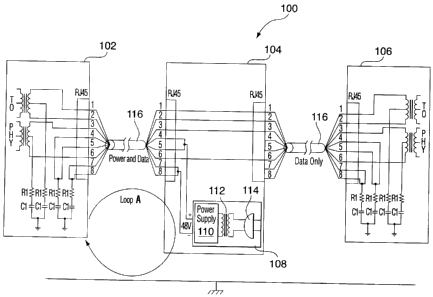
Fig. 1 illustrates a system 100 in which a conventional IP phone 102 is
coupled to
a known midspan power adapter 104, which is in turn coupled to a network
switch 106.
The midspan power adapter 104 includes, or is otherwise connected to or in
electrical
communication with, a power source 108. The power source 108 in Fig. 1 is
connected
between device connector wire pairs 4,5 and 7,8. The power source 108 is
typically 48
volts DC, and can comprise one or more batteries, or an uninterruptible power
supply
(UPS). More typically, and as shown in Fig. 1, the power source comprises an
AC
adapter which can plug into a typical wall outlet. The AC adapter can include
a power
supply 110, a transformer 112, and a wall plug 114. Connection between the IP
phone
102, the midspan power adapter 104, and the network switch 106 is
conventionally
enabled by cabling 116, such as Category 5, or CATS, cabling. Different
categories of
cabling can be used for different equipment, such as 10/100/1000 Mbps
Ethernet, also
known respectively as 10/100/1000 Base-T, with 1000 Mbps Ethernet also being
known
as Gigabit Ethernet.
Midspan power adapters typically feed the signal wires directly through a
first set
of wires, identified as wires 1 to 3 and 6 in Fig. 1. Power is injected on the
phone (or
powered device) side from the power source 108 via spare pairs, shown as pairs
4,5 and
7,8 in Fig. 1. On the switch side, the spare wires are usually unterminated.
Cutting the
spare pairs to insert power, and not properly terminating the pairs
significantly changes
the common mode impedance between each pair within the cable. This
discontinuity
alters the balance and symmetry of the cable, causing an increase in radiated
emissions
when a midspan power adapter is used with an IP phone. Thus the powered device
may
exceed emission limits when in operation. The design intent for powered
Ethernet
devices, such as IP phones, is to have minimal electro-magnetic emissions.
Discontinuities such as those encountered in midspan PoE adapters can
significantly
elevate emission levels.
It is possible to provide power to an end device without breaking or cutting
the
spare pairs inside the midspan power adapter. However, there is no way of
knowing what
the spare pairs are connected to at the network switch 106. For example, if a
resistive
load is attached at the network switch 106, placing power on the spare pair
could destroy
2
CA 02545525 2006-05-02
the load. For this reason, a break in the spare pairs is generally provided in
a midspan
power adapter. Unfortunately, this break also causes an increase in the amount
of
radiated energy.
Several methods exist for containing unwanted emissions. One approach is to
add
a common mode filter clamp on an Ethernet cable to be used with a powered
device.
This involves customers placing chokes on cables which often does not occur,
and
makes cable management difficult since the chokes can be bulky. Alternatively,
a choke
could be moulded onto the cable, but this can be costly and standard
replacement cables
cannot be used. Another approach is to add common mode chokes within the
powered
device either as discrete parts or embedded into the Ethemet connectors. A
further
approach is to use shielded cable throughout any links containing a midspan
power
adapter. Shielded cable, however, is more expensive and not as commonly used
as the
Unshielded Twisted Pair Category 5 Ethernet cable specified for use with IP
Phones
today. Rewiring a building tends to be cost prohibitive.
In general, these approaches merely add extra filtering and cost to each IP
phone,
rather than fixing the source of the problem. The problem lies in the midspan
power
adapter and the radiated energy it causes.
It is, therefore, desirable to provide a midspan power adapter that can power
an IP
device without adding significant radiated energy to the system.
SUMMARY OF THE INVENTION
It is an object of the present invention to obviate or mitigate at least one
disadvantage of previous midspan power adapters for use with a powered device,
end
device or IP device.
This invention provides a midspan PoE adapter with reduced emission levels
when compared with conventional implementations of midspan PoE adapters.
In a first aspect, the present invention provides a midspan power adapter to
power
a powered device in a balanced cable system. The power adapter has a device
side
including device connectors and a system side including system connectors, as
well as a
power source provided between two spare pairs of the device connectors. The
adapter
includes a common mode choke connected inline between the power source and the
spare pairs of the device connectors. The adapter also includes a transformer
to isolate
the device connectors and the system connectors. The transformer has device
side
terminals connected to signal pairs of the device connectors and system side
terminals
connected to signal pairs of the system connectors. The transformer also has
first center
taps and second center taps. The adapter further includes a termination
network
3
CA 02545525 2006-05-02
connected between non-signal connectors and a common point to provide common
mode
termination. The adapter also includes a common mode choke connected to the
termination network to provide power from the power source to a pair of device
connectors.
In an embodiment, the non-signal connectors include the first center taps of
the
transformer, spare pairs of the device connectors and spare pairs of the
system
connectors. The adapter can further include a phantom power common mode choke
to
provide power from a power supply to the second center taps on the
transformer. In
another embodiment, the non-signal connectors include the second center taps
of the
transformer, in which case the termination network terminates the first and
second center
taps to a common point. The common mode choke can be connected to a spare pair
of
device connectors. The termination network can include a plurality of common
mode
terminations each having substantially similar resistance and capacitance
values. The
resistance values can be determined in accordance with pair-to-pair common
mode
impedance within a connector cable. The termination network can include a Bob
Smith
Termination. The termination network can include a first termination network
for
terminating the end device connectors and system connectors, and a second
termination
network for terminating the first center taps. The transformer can be a 1:1
isolation
transformer, the balanced cable system can be an Ethernet system, and the
powered
device can be an Internet protocol (IP) device.
Other aspects and features of the present invention will become apparent to
those
ordinarily skilled in the art upon review of the following description of
specific
embodiments of the invention in conjunction with the accompanying figures.
BRIEF DESCRIPTION OF THE DRAWINGS
Embodiments of the present invention will now be described, by way of example
only, with reference to the attached Figures, wherein:
Fig. 1 illustrates an Internet phone system including a midspan power adapter;
Fig. 2 illustrates an Internet phone system including a midspan power adapter
according to an embodiment of the present invention;
Fig. ~ illustrates a midspan power adapter according to another embodiment of
the present invention;
Fig. 4 is a frequency plot of radiated emissions from an Internet phone system
powered from an endspan device (no midspan adapter); and
Fig. 5 is a frequency plot of radiated emissions from an Internet phone system
including a conventional midspan power adapter; and
4
CA 02545525 2006-05-02
Fig. 6 is a frequency plot of radiated emissions from an Internet phone system
including a midspan power adapter according to an embodiment of the present
invention.
DETAILED DESCRIPTION
Generally, the present invention provides a midspan power adapter for use in a
balanced communication system, such as an Ethernet system, where differential
signals
are transmitted between two devices. The adapter of the invention passes data
signals
through, and provides power to an end device, such as an IP phone, with
significantly
less contribution to the electromagnetic emissions of the system than
conventional
midspan adapters. The adapter of the invention can provide power through
separate
unused wires (known as spare pair power in Ethernet systems) or by combining
power
with data signals (otherwise known as phantom feed). A common mode choke is
included
in the power feed to prevent noise currents from flowing through the power
supply
connections to earth ground, helping to minimize radiated noise. The midspan
power
adapter also includes a transformer having first and second center taps. Using
proper
common mode terminations to a common point from the center taps and the spare
pairs
of both the incoming and outgoing cables, the balance and symmetry inherent in
a
structured cable, such as those found in Ethernet communication systems, can
be
maintained. Maintaining this balance and symmetry reduces the amount of wanted
differential signal energy that is converted to common mode energy which leads
to
radiated emissions.
A common mode signal is, strictly speaking, the average of the signals present
at
the two inputs of a differential amplifier. A common mode signal also refers
to the voltage
level present at both inputs of a differential amplifier, as if they were tied
together.
Common mode impedance is an impedance seen when testing into a pair of lines
driven
by identical (common) signals.
The present invention provides an enhancement to current implementations of a
Midspan Power Over Ethernet Adapter. It can be used in a balanced system, such
as a
100 Base-T or Gigabit Ethernet system. Current midspan adapters cause
significant
energy to be radiated off of an attached Ethernet cable carrying data signals.
A midspan
power adapter according to the present invention assists in meeting emission
limits for
any powered device, such as an IP Phone, connected to the adapter. The
emission limits
can be defined by IEC CISPR 22 Class B, or similar requirements such as FCC
Class B.
Integrating the solution directly into a Midspan Power Over Ethernet Adapter
shifts the
cost from the powered device (IP Phone) to the Adapter, which is the source of
the
problem.
CA 02545525 2006-05-02
To reduce the amount of energy being radiated by a cable carrying 100 Base-T
signaling, the amount of common mode current carried on the cable can be
reduced. A
midspan power device of the present invention maintains cable symmetry and
balance by
properly terminating both the incoming and outgoing cables within the adapter,
and adds
common mode impedance to the power feed. Current solutions simply leave the
spare
pairs on the incoming cable floating, or unterminated, and do not properly
maintain the
common mode impedance between each pair; a part of the intended differential
mode
signal on the cable is thus converted to common mode energy, which leads to
increased
radiated energy.
The present invention also provides midspan power in a novel manner. A
galvanic
device, such as a transformer, is included in the midspan power adapter to
maintain
isolation and supply power to the powered device without presenting power to
the
network switch or the rest of the network. The transformer provides power and
maintains
isolation, while at the same time maintaining signal integrity within the
cable, without
adding radiated noise. While it is presently believed that a transformer
provides the best
isolation, diodes or capacitors can also be used. The transformer is
preferably a
transformer having a one-to-one winding ratio. Other transformer winding
ratios can be
used, but such a change would affect the Ethernet signal and would not provide
maximum power transfer as will a winding ratio of 1 to 1. A different
transformer winding
ratio can be used in order to compensate for a mismatch, such as an impedance
mismatch.
The present invention counterintuitively addresses an electromagnetic
compatibility (EMC) issue. Intuitively, a designer would not add another
component to the
adapter, as it would adversely affect the main data signal. Clearly, adding a
transformer in
the midspan power adapter adds an insertion loss. This added insertion loss
can reduce
the maximum cable length, or span, between the powered device and the system.
However, unexpectedly, the radiated emissions are minimized.
While there are some known approaches that claim a device is FCC (or IEC)
Class B compliant, those compliance tests generally only test the power
supply, and do
not include putting 100 Mbps Ethernet signaling through the adapter during the
test. The
present invention is meant to address the energy radiated due to the Ethernet
signaling
passing through the adapter.
One known approach deals with the coupling of power with a data signal using a
transformer. However, that approach does not use common mode terminations on
the
center taps of the transformer, and does not return common mode currents to a
common
reference point. This does not consider the problem of radiated emissions.
Moreover, the
6
CA 02545525 2006-05-02
configuration results in discontinuities, which are addressed by the present
invention.
Known midspan devices do not provide proper common mode terminations of spare
pairs
with respect to signal pairs for maintaining low levels of radiated emissions.
Fig. 2 illustrates an Internet phone system 200, including a midspan power
adapter 202 according to an embodiment of the present invention. The phone
102,
network switch 106 and cabling connections 116 in Fig. 2 are generally similar
to those
shown in Fig. 1. In the new adapter 202, a transformer 204, such as a 1:1
isolation
transformer, is used to pass a data signal, such as a 100 Base-T signal. The
transformer
204 logically separates the midspan power adapter into two separate cables or
sides: a
device side 206 having device connectors 208, and a system side, or switch
side, 210
having system connectors 212. Signal pairs of the device connectors are
connected to
device side terminals of the transformer, and signal pairs of the system
connectors are
connected to system side terminals of the transformer. The logical separation
into two
separate sides permits proper consideration of balancing and symmetry of the
cable.
Balance and symmetry help to control radiated emissions when the midspan power
adapter is used with an IP phone.
Rather than feeding the signal pairs straight through, center taps 214 of the
transformer 204 are used to properly terminate signal pairs from a common mode
perspective via a first termination network 216, in order to maintain the
impedance
between signal pairs and spare pairs. The spare pairs are also connected to a
common
mode termination via a second termination network 218, such as a DC blocking
capacitor
and a resistor. All terminations for both incoming and outgoing cables are
preferably
connected to a common point 220. Although the termination networks 216 and 218
are
discussed separately in order to distinguish the points that they connect
together, the
termination networks themselves are generally the same as each other, as
illustrated in
Fig. 2. Considering both termination networks as a single termination network,
it can be
described as being connected between non-signal connectors and a common point
to
provide common mode termination. The non-signal connectors can include first
center
taps of the transformer, spare pairs of the device connectors and spare pairs
of the
system connectors.
The center taps 214 can also be referred to as first and second center taps,
as
they will be in another embodiment. In the embodiment of Fig. 2, the
termination network
terminates both the first center taps and second center taps to the common
point 220.
The first and second termination networks 216 and 218 preferably have
substantially similar resistance and capacitance values. Keeping all resistors
at
substantially similar values provides the desired symmetric impedance between
pairs,
7
CA 02545525 2006-05-02
and improves cable balance over current implementations. Resistor values can
be
determined in accordance with the pair-to-pair common mode impedance within
the
cable. The selection of resistor values can be determined in accordance with
the Bob
Smith Termination technique described in United States Patent No. 5,321,372
issued on
June 14, 1994 and entitled "Apparatus and method for terminating cables to
minimize
emissions and susceptibility". Variations on that technique are described in
"Updating the
Bob Smith Termination Technique", by Jim Satterwhite of Teltest Electronic
Laboratories
at http://www.commsdesign.com/design
corner/showArticle.jhtml?articlelD=19300046.
Different types of cable require different termination resistor values. The
invention
described herein can be used with other types of cable (such as Category 6
cable) by
selecting appropriate resistor values.
By providing termination networks 216 and 218, noise currents are contained
within the cable. The present invention sends noise back to its source so that
it forms the
smallest loop area (Loop B in Fig. 2), i.e. its antenna size is minimized. If
a noise signal
is allowed to radiate over a large loop (Loop A in Fig. 1), the result is a
large antenna.
This is the result when antenna pairs, or wire pairs, are broken such as shown
in Fig. 1.
The return path for noise currents in a system as in Fig. 1 is via earth
ground. The
transformer configuration according to an embodiment of the present invention
in Fig. 2
maintains the symmetry and coupling of the Ethernet signal within the cable
itself.
Power is added to the spare pair on the outgoing cable through a common mode
choke 222. This power is typically from a power source 224, such as a DC power
source
suitable for powering a powered device, such as an IP phone. In Ethernet
applications, a
48 Volts DC power source is often employed. Variations in implementation of
the power
source 224 are similar to those of the previously described power source 108.
The
common mode choke 222 contains the noise currents within the Ethernet cable
rather
than having them flow through the power supply connection to earth ground.
This
essentially reduces the effective area of radiation. Also, without a common
mode choke,
connecting the power source, or power supply, across the spare pairs causes
the
common mode impedance between those pairs to be much lower than desired. The
common mode choke 222 in the power feed looks like a high impedance, making
the
termination impedance the low impedance common mode path between the pairs.
This
restores a symmetric common mode impedance between the pairs which reduces the
conversion of desired differential signal (data) energy into common mode
energy.
In other words, an embodiment of the present invention provides a midspan
power
adapter to power a powered device in a balanced cable system. The power
adapter has a
device side including device connectors and a system side including system
connectors,
8
CA 02545525 2006-05-02
as well as a power source provided between two spare pairs of the device
connectors.
The adapter includes a transformer to isolate the device connectors and the
system
connectors. The transformer has device side terminals connected to signal
pairs of the
device connectors and system side terminals connected to signal pairs of the
system
connectors. The adapter also includes a termination network that is connected
between
non-signal terminals of both the transformer and the connectors and a common
point, to
provide common mode termination. The adapter also includes a common mode choke
connected inline between the power source and the spare pairs of the device
connectors.
The non-signal terminals can include center taps of the transformer, spare
pairs of the
device connectors and spare pairs of the system connectors.
Power can be fed to the midspan power adapter via the spare pairs or via the
center taps. In the embodiment of Fig. 2, power is shown as being provided
across the
spare pairs on the phone or device side of the midspan power adapter. Feeding
power
into the center taps of the transformer, on the differential pairs to the end
device, is also
known as a phantom feed. Fig. 3 illustrates a midspan power adapter according
to
another embodiment of the present invention. Providing power via phantom feed,
as
illustrated in Fig. 3, has not been done in the past because it requires a
transformer
which adds cost and reduces the transmission range slightly by adding some
insertion
loss in the link. In this case the spare pairs are left connected together
through the
adapter and the supply voltage only appears on the end device side of the
transformer.
The midspan power adapter 302 shown in Fig. 3 includes means to feed power to
the spare pairs (as in Fig. 2) and means to feed power via the center taps,
i.e. phantom
feed. The network or system side center taps that remain only connected to the
common
point can be referred to as first center taps. This embodiment includes a
phantom power
common mode choke 304 to provide power from a power supply to second center
taps,
or phantom power center taps, of the transformer. The phantom power common
mode
choke 304 is provided in addition to the existing termination network. The
remaining
components and connections in Fig. 3 are substantially similar to Fig. 2, and
reference is
made to the description of Fig. 2 for further information.
Fig. 4 is a frequency plot of radiated emissions for an Internet phone powered
from an endspan power system using phantom feed. Since there is no midspan
device in
this arrangement, there is no emissions contribution associated with midspan
devices.
The measurements were taken with a biconical log antenna in the vertical
orientation. For
reference, the CISPR22 Class B boundary 402 is highlighted. The frequency
range of
interest is from 50 MHz to 150 MHz where a spectrum of the MLT-3 coding used
in
100Mbps Ethernet signaling resides. (The peak in the range of 100-200 MHz is
an
9
CA 02545525 2006-05-02
unrelated issue and will not be discussed herein.) The illustration in Fig. 4,
particularly
radiated emissions plot 404, is provided as a reference to show the level of
emissions the
phone can achieve.
Fig. 5 illustrates a frequency plot 502 of radiated emissions from the same IP
phone as in Fig. 4, but this time powered from a conventional midspan power
adapter,
rather than an endspan power system. Again, the Class B boundary 402 is shown
for
reference in Fig. 5. The radiated emissions from 50 to 150MHz in Fig. 5 are
generally
much higher than with the phone powered by an endspan device as in Fig. 4.
Fig. 6 is a frequency plot of the same phone as in Fig. 4, this time powered
from a
midspan power adapter according to an embodiment of the present invention.
Again, the
measurements were taken with the antenna in the vertical configuration.
Emitted radiation
for this configuration is shown as 602, and the Class B boundary 402 is again
included for
reference. Comparing the emission levels between 50 and 150MHz, the results in
Fig. 6
are nearly as good as the "baseline" case of Fig. 4. While the system in Fig.
6 includes
an 1P phone and a midspan power adapter according to an embodiment of the
invention,
the system in Fig. 4 includes an IP phone powered from an endspan device (i.e.
no
midspan contribution). The emission results in Fig. 6 are significantly
improved over the
results from implementation of a conventional midspan adapter, as shown in
Fig. 5.
Improvements can be observed with respect to lower emission energy when viewed
as a
whole, as well as with respect to the peaks being farther away from the limit
lines.
There is a tradeoff of reduced maximum cable span between the powered device
and the network switch, since adding a transformer in the Ethernet link will
add some
small insertion loss. However, a system according to the invention reduces
emissions
when compared with conventional midspan power systems, and removes the need to
provide power over separate wires to the powered device.
The midspan power adapter of the present invention can be used with any
Ethernet device. Examples include a wireless base station or Ethernet base
station.
Midspan power adapters are popular in the home-office or tele-working
environment.
Embodiments of the present invention can be used in connection with 100-base-T
Ethernet as well as with Gigabit Ethernet. The embodiment shown in Fig. 2 is
provided
for use with a 100 MB Ethernet. In a Midspan Power Over Ethernet Adapter for
Gigabit
Ethernet applications, all four pairs are preferably routed through the
transformer, and all
center taps are terminated in the same manner as center taps A and B in Fig.
3.
Although a single port midspan power adapter has been described and
illustrated
herein, embodiments of the present invention can be implemented as a multiport
midspan
power adapter as will be apparent to one of ordinary skill in the art.
CA 02545525 2006-05-02
The midspan power adapter of the present invention can be used with any
balanced cable system, including Ethernet, with the resistor values in the
termination
networks chosen to provide appropriate impedance. The embodiments of the
present
invention can be used with a balanced system wherein a differential signal is
transmitted.
By powering the system, the symmetry of the common mode impedance between
pairs is
broken by the power injecting product. Examples of non-Ethernet balanced
systems
include RS 422 and RS 485.
The above-described embodiments of the present invention are intended to be
examples only. Alterations, modifications and variations may be effected to
the particular
embodiments by those of skill in the art without departing from the scope of
the invention,
which is defined solely by the claims appended hereto.
11