Note: Descriptions are shown in the official language in which they were submitted.
CA 02545630 2006-05-11
WO 2005/052564 PCT/US2004/038665
MINIATURIZED MULTI-GAS AND VAPOR SENSOR DEVICES
AND ASSOCIATED METHODS OF FABRICATION
FIELD OF THE INVENTION
The invention relates generally to the field of miniaturized sensor devices
and
platforms and, more specifically, to the field of nano and pico-scale
sensor.devices
and platforms. An aspect of the invention provides robust, high-sensitivity,
hi~gh-
selectivity, high-stability multi-gas and vapor sensor devices, among other
sensor
devices, and associated methods of fabrication. Variants of the multi-gas and
vapor
sensor devices of the invention may be used for the in situ measurement of
soluble
analytes in liguid media. Another aspect of the invention provides a thermally-
isolated micro-platfornl for such microelectromechanical systems (MEMS). A
further
aspect of the invention provides a design for wide-dynamic range, micro-
machined
humidity sensor devices, among other sensor devices, that relieves the
generated
stresses in the associated sensing films caused by sensing film swelling due
to the
adsorption of water. A still further aspect of the invention provides a
protocol for the
deposition of self assembled monolayers (SAMs) as multi-gas and vapor 'sensing
films.
BACKGROUND OF THE INVENTION
The scientific and technological interest in miniaturized gas, humidity,
chemical,
temperature, and pressure sensor devices has grown in recent years. The need
for
such devices spans a wide range of industries and applications, such as the
medical
instrumentation, food and agriculture, paper, automotive, electric appliance,
petrochemical, and semiconductor industries, as well as the military, in, for
example,
gas, humidity, chemical, temperature, and pressure sensing applications. The
wide
range of environments to which these devices may be exposed severely limits
the
candidate materials that may be used to build the devices. A number of gas,
humidity,
chemical, temperature, and pressure sensor devices have been developed and
built for
CA 02545630 2006-05-11
WO 2005/052564 PCT/US2004/038665
specific applications. However, none of these devices demonstrate a suitable
combination of the desired robustness, sensitivity, selectivity, stability,
size,
simplicity, reproducibility, reliability, response time, resistance to
contaminants, and
longevity. Thus, what are still needed, in general, are mufti-gas and vapor
sensor
devices, among other sensor devices, that exploit the high sensitivity of
differential
scanning nano and picocalorimetry microelectromechanical systems (MEMS) to
heat
flow and the unique propeuties of certain thin films and nano and
picoparticles,
including their high adsorption potential, high adsorption rate under
optimized
conditions, high desorption rate under optimized conditions, high chemical
stability,
and heat release associated with the physisorption of gas and vapor molecules.
Response time, mechanical strength, power consumption, and crosstalk between
unit
sensor devices are major areas of concern with respect to thermally-sensitive
microelectromechanical systems (MEMS), such as gas, humidity, chemical,
temperature, and pressure sensor devices, as well as calorimeter and
microheater
devices, in general. For example, faster response time provides higher
sensitivity and
greater mechanical strength provides higher reliability. Likewise, lower power
consumption is desired for portable and wireless devices and less crosstalk
between
unit sensor devices provides greater accuracy. Response time and sensitivity
are
critical in many sensing applications, such as in sensing for warfare agents,
measuring
low dew points, detecting trace gases, etc., but are difficult to optimize
with
conventional mufti-gas and vapor sensor devices without making sacrifices with
respect to other performance parameters. Power consumption and crosstalk
between
unit sensor devices are both affected by thermal isolation. Typically, thermal
isolation has been addressed by fabricating microelectromechanical systems
(MEMS)
on thin insulating membranes with low heat capacity. However, such thin
membranes
are fragile, resulting in low yield and reliability problems. Moreover, the
peripheries
of these thin membranes are typically bonded to a silicon substrate,
introducing lateral
heat conduction losses. Thus, what are needed are microelectromechanical
systems
(MEMS) that are built with, for example, low-thernal conductivity regions
around the
active thin membrane regions, resulting in more robust, high-performance, high-
sensitivity microelectromechanical systems (MEMS).
2
CA 02545630 2006-05-11
WO 2005/052564 PCT/US2004/038665
Two additional areas of concern are raised with respect to miniaturized vapor
(e.g:,
humidity) sensor devices, among other sensor devices. First, the polymeric
sensing
films associated with such vapor sensor devices often become significantly
swollen
while at relatively high humidity due to their high affinity for water vapor.
The
swelling of these sensing films generates lateral stresses that impinge upon
the thin'
membranes, potentially breaking them. Second, sensing films having larger
surface
areas are desired in order to reduce the thickness of the sensing films at a
given mass.
Reducing the thickness of the sensing films and incorporating nanostructures
(e.g.,
nano-spheres, nano-rods, nano-fibers, etc.) into the senszng materials
decreases the
diffusion time constant of the water adsorption/desorption, reducing the
response time
of the vapor sensor devices. Thus,,what are needed are micro-machined vapor
sensor
devices, among other sensor devices, that utilize, for example, high-aspect
ratio
silicon microstructures etched' adjacent to the thin membranes. These silicon
microstructures would serve as stress relievers at varying vapor (e.g.,
humidity) levels
and provide both large surface areas for the sensing films, increasing the
sensitivity of
the vapor sensor devices, and effective heat conduction paths to the
microheaters also
disposed adjacent to the thin membranes. '
BRIEF SUMMARY OF THE INVENTION
In various embodiments, the invention provides robust, high-sensitivity, high-
selectivity, high-stability multi-gas and vapor sensor devices and platforms,
among
other sensor devices and platforms, and associated methods of fabrication. The
multi-
gas and vapor sensor devices exploit the high sensitivity of differential
scanning nano
and picocalorimetry microelectromechanical systems (MEMS) to heat flow and the
unique properties of certain thin films and nano and picoparticles, such as
zeolite thin
films and nano and picoparticles, as well as porous ceramics, crosslinked
polyelectrolytes, aluminosilicates, and carbon nanotubes, including their high
adsorption potential, high adsorption rate under optimized conditions, high
desorption
rate under optimized conditions, high chemical stability, and heat release
associated
with the physisorption of gas and vapor molecules. The origins of this heat
release
are the energy conversions associated directly with the adsorption of a sensed
3
CA 02545630 2006-05-11
WO 2005/052564 PCT/US2004/038665
substance, as well as any secondary thermal transitions characteristic of the
dry
material.
In various embodiments, the invention also provides a thermally-isolated micro-
platfonn for robust, high-performance, high-sensitivity microelectromechanical
systems (MEMS). Using various micro-machining techniques, microstructures with
low thermal conductivities are incorporated into the ' peripheries of active
thin
membrane areas, the thermally-sensitive microelectromechanical systems (MEMS)
disposed on either side of, the thin membranes. The resulting thermal
isolation
provides faster response time, greater mechanical strength, lower power
consumption,
and less crosstalk between unit sensor devices than is possible with a purely
thin
membrane-based design.
In various embodiments, the invention further provides micro-machined vapor
(e.g.,
humidity) sensor devices, among other sensor devices, that utilize high-aspect
ratio
silicon microstructures etched adjacent to the thin membranes. These high-
aspect
ratio silicon microstructures serve as stress relievers due to the large
Young's
modulus coefficient of silicon. By varying the dimensions of the silicon
microstructures, different spring constants may be achieved, accommodating the
generated stresses caused by the swelling problems described above at varying
vapor/humidity levels. The silicon microstructures provide both large surface
areas
for the sensing films, increasing the sensitivity of the vapor sensor devices,
and
effective heat conduction paths to the microheaters also disposed adjacent to
the thin
membranes. Another method for alleviating the stresses resulting from the
adsorption
of water vapor by intensely hydrophilic organic polymer materials is provided,
involving the creation of a self assembled monolayer (SAM) with
polyelectrolyte
functionality on a highly-reticulated substrate of silicon oxide which has
been vapor
deposited onto the thermally-conductive membrane of a hot plate.
In one specific embodiment of the invention, a miniaturized sensor device
includes a
thin film membrane having a first surface and a second surface, one or more
resistive
thin film heater/thennometer devices disposed directly or indirectly adjacent
to the
first surface of the thin film membrane, and a frame disposed directly or
indirectly
4
CA 02545630 2006-05-11
WO 2005/052564 PCT/US2004/038665
adjacent to the second surface of the thin film membrane, wherein one or more
internal surfaces of the frame define at least one cell having at least one
opening. The
sensor device also includes a thin film layer disposed directly or indirectly
adjacent to
the frame. The sensor device further includes a sensing layer disposed
directly or
indirectly adjacent to the thin film membrme.
In another specific embodiment of the invention, a method for fabricating a
miniaturized sensor device includes providing a silicon layer having a first
surface
and a second surface, depositing a first thin film layer having a first
surface and a
second surface on the first surface of the silicon layer, and depositing a
second thin
film layer on the second surface of the silicon layer. The method also
includes
masking the first surface of the first thin film layer and selectively
depositing a
sacrificial layer on the first surface of the first thin film layer, wherein
the sacrificial
layer defines one or more exposed regions of the first surface of the first
thin film
layer. The method further includes depositing a conductive layer on a surface
of the
sacrificial layer and the one or more exposed regions of the first surface of
the first
thin film layer defined by the sacrificial layer and removing the sacrificial
layer and. a
portion of the conductive layer deposited on the surface of the sacrificial
layer to form
one or more resistive thin film heater/thermometer devices on the first
surface of the
first thin film layer. The method still further includes selectively removing
a portion
of the second thin film layer and selectively removing a portion of the
silicon layer to
form at least one cell, wherein the at least one cell is disposed directly or
indirectly
adjacent to the second surface of the first thin film layer, and wherein the
cell is
substantially aligned with the one or more resistive thin film
heater/thermometer
devices. The method still further includes disposing a sensing layer on the
second
surface of the first thin film layer.
In a further specific embodiment of the invention, a microelectromechanical
system
includes a thin film membrane having one or more active membrane areas and one
or
more inactive membrane areas. The microelectromechanical system also includes
one
or more resistive thin film heater/thermometer devices disposed directly or
indirectly
adjacent to the one or more active membrane areas of the thin film membrane.
The
microelectromechanical system further includes a fi-ame disposed directly or
CA 02545630 2006-05-11
WO 2005/052564 PCT/US2004/038665
indirectly adjacent to the one or more inactive membrane areas of the thin
film
membrane. The microelectromechanical system still further includes one or more
low-thermal conductivity microstructures disposed between the one or more
active
membrane areas of the thin film membrane and the one or more inactive membrane
areas of the thin film membrane.
In a still further specif c embodiment of the invention, at miniaturized
sensor device
includes a thin film membrane having one or more active membrane areas and one
or
more inactive membrane areas, one or more resistive thin film
heater/thermometer
devices disposed directly or indirectly adjacent to the one or more active
membrane
areas of the thin film membrane, and a frame disposed directly or indirectly
adjacent
to the one or more inactive membrane areas of the thin film membrane. The
sensor
device also includes one or more low-thermal conductivity microstructures
disposed
between the one or more active membrane areas of the thin film membrane and
the
one or more inactive membrane areas of the thin film membrane. The sensor
device
further includes one or more stress relief structures disposed directly or
indirectly
adjacent to the one or more active membrane areas of the thin film membrane.
The
sensor device still further includes one or more sensing films disposed
directly or
indirectly adjacent to the one or more stress relief structures.
BRIEF DESCRIPTION OF THE DRAWINGS
Figure 1 is a cross-sectional side view of two related embodiments of the
sensor
device of the invention, the sensor device consisting of a multi-cell ultra
high-
sensitivity differential scanning calorimeter (UHSDSC), which is a
microelectromechanical system (MEMS);
Figure 2 is a cross-sectional side view of the sensor device of Figure 1,
highlighting
the addition of a thin film or nanoparticle layer to one or more cells of the
sensor
device;
Figure 3 is a cross-sectional side view of another embodiment of the sensor
device of
the invention, highlighting the use of one or more grids operable for Keeping
6
CA 02545630 2006-05-11
WO 2005/052564 PCT/US2004/038665
particulates and/or contaminants away from the one or more thin film or
nanoparticle
layers of Figure 2;
Figure 4 is a cross-sectional side view of one embodiment of a packaging
assembly
for the sensor devices of Figures 1-3;
Figure 5 is a cross-sectional side view illustrating a first step in the
fabrication of the
sensor device of Figure 1;
Figure 6 is a cross-sectional side view illustrating a second step in the
fabrication of
the sensor device of Figure 1;
Figure 7 is a cross-sectional side view illustrating a third step in the
fabrication of the
sensor device of Figure 1;
Figure 8 is a cross-sectional side view illustrating a fourth step in the
fabrication of
the sensor device of Figure 1;
Figure 9 is a cross-sectional side view illustrating a fifth step in the
fabrication of the
sensor device of Figure 1;
Figure 10 is a cross-sectional side view illustrating a sixth step in the
fabrication- of
the sensor device of Figure 1;
Figure 11 is a cross-sectional side view illustrating a seventh step in the
fabrication of
the sensor device of Figure l;
Figure 12 is a top planar view and a cross-sectional side view of one
embodiment of
the thermally-isolated micro-platform for microelectromechanical systems
(MEMS)
of the invention, highlighting the use of a trench refill approach using a
dielectric
material and high-aspect ratio trenches (HARTs) or grids;
Figure 13 is a cross-sectional side view illustrating the first step of the
trench refill
approach using a dielectric material and high-aspect ratio trenches (HARTs) or
grids
of Figure 12;
7
CA 02545630 2006-05-11
WO 2005/052564 PCT/US2004/038665
Figure 14 is a cross-sectional side view illustrating the second step of the
trench refill
approach using a dielectric material and high-aspect ratio trenches (HARTS) or
grids
of Figure 12;
Figure 15 is a cross-sectional side view illustrating the third step of the
trench refill
approach using a dielectric material and high-aspect ratio trenches (HARTS) or
grids
of Figure 12;
Figure 16 is a cross-sectional side view illustrating the fourth step of the
trench refill
approach using a dielectric material and high-aspect ratio trenches (HARTS) or
grids
of Figure 12;
Figure 17 is a cross-sectional side view illustrating the fifth step of the
trench refill
approach using a dielectric material and high-aspect ratio trenches (HARTs) or
grids
of Figure 12;
Figure 18 is a top planar view and a cross-sectional side view of another
embodiment
of the thermally-isolated micro-platform for microelectromechanical systems
(MEMS) of the invention, highlighting the use of a thick oxide approach using
the
thermal oxidation of high-aspect ratio trenches (HARTS) or grids;
Figure 19 is a cross-sectional side view illustrating the first step of the
thick oxide
approach using the thermal oxidation of high-aspect ratio trenches (HARTS) or
grids
of Figure 18;
Figure 20 is a cross-sectional side view illustrating the second step of the
thick oxide
approach using the thermal oxidation of high-aspect ratio trenches (HARTs) or
grids
of Figure 18;
Figure 21 is a cross-sectional side view illustrating the third step of the
thick oxide
approach using the thermal oxidation of high-aspect ratio trenches (HARTS) or
,grids
of Figure 18;
8
CA 02545630 2006-05-11
WO 2005/052564 PCT/US2004/038665
Figure 22 is a cross-sectional side view illustrating the fourth step of the
thick oxide
approach using the thermal oxidation of high-aspect ratio trenches (HARTS) or
grids
of Figure 18;
Figure 23 is a cross-sectional side view illustrating the fifth step of the
thick oxide
approach using the thermal oxidation of high-aspect ratio trenches (HARTS) or
grids
of Figure 18;
Figure 24 is a cross-sectional side view of two related embodiments of the
micro-
machined humidity sensor device of the invention that utilizes high-aspect
ratio
silicon microstructures adjacent to the thin membranes, highlighting the
sensing film
prior to water adsorption;
Figure 25 is a cross-sectional side view of the micro-machined humidity sensor
device
of Figure 24, highlighting the sensing film subsequent to water adsorption;
Figure 26 is a cross-sectional side view of another embodiment of the micro-
machined humidity sensor device of the invention that utilizes' high-aspect
ratio
silicon microstructures adjacent to the thin membranes, highlighting the
sensing film
prior to water adsorption; and
Figure 27 is a cross-sectional side view of the micro-machined humidity sensor
device
of Figure 26, highlighting the sensing film subsequent to water adsorption.
DETAILED DESCRIPTION OF THE INVENTION
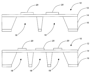
Referring to Figure 1, the sensor device 10 of the invention, which may be a
mufti-gas
or vapor (e.g., humidity) sensor device, among other sensor devices, consists
of a
mufti-cell ultra high-sensitivity differential scanning calorimeter (UHSDSC),
which is
a microelectromechanical system (MEMS). The sensor device 10 is fabricated
using
standard silicon processing techniques, well known to those of ordinary skill
in the
art. The sensor device 10 includes a thin, thermally-insulating silicon
oxinitride
(SiONx) membrane 12 disposed directly adjacent to a silicon (Si) frame 14. It
should
be noted that other suitable materials may replace the silicon oxinitride
membrane 12
andlor the silicon frame 14. For example, the silicon oxinitnde membrane 12
may be
9
CA 02545630 2006-05-11
WO 2005/052564 PCT/US2004/038665
replaced with a silicon, polysilicon, parylene, or polyimide membrane.
Preferably, a
thin silicon oxinitride layer 16 is also disposed directly adjacent to the
silicon frame
14 opposite the silicon oxinitride membrane 12. Again, other suitable
materials may
replace the silicon oxinitride layer 16. Preferably, the sensor device 10 has
an overall
length of between about 0.5 mm and about 3 cm, and an overall width of between
about 0.5 mm and about 3 cm, although other suitable dimensions may be used.
Preferably, the silicon oxinitride membrane 12 has a thickness of between
about 50
nm and about 1 micron, although other suitable dimensions may be used.
Specifically, the thickness of the silicon oxinitride membrane 12 may be
varied
depending upon the materials) used andlor the sensitivity desired.
'Preferably, the
silicon frame 14 has a thickness of between about 50 microns and about 650
microns,
although other suitable dimensions may be used. The silicon frame 14 divides
the
sensor device 10 into two or more cells 18, which are ideally identically
symmetric
and identical. One of the cells 18 may be used as a reference cell during
operation,
while the other cells 18 may be used as sensing cells. A plurality of thin
film
heater/thermometers 20 are disposed directly adjacent to the silicon
oxinitride
membrane 12 opposite the silicon frame 14. Preferably, the location of each of
the
plurality of thin film heater/thermometers 20 generally corresponds to each of
the two
or more cells 18. The plurality of thin film heater/thermometers 20 may be
made of
platinum (Pt) and/or titanium (Ti), although other suitable materials may be
used,
such as gold (Au) and/or chromium (Cr), gold and/or nickel (Ni) and/or copper
(Cu),
aluminium (Al), etc., as well as polysilicon, heavily-doped silicon, silicon
carbide, etc.
Advantageously, the silicon oxinitride membrane 12 allows rapid heat
propagation in
the z-direction, to and from the plurality of thin film heater/therlnometers
20. It
should be noted that the layout and configuration of the sensor device 10
illustrated in
Figure 1 is exemplary only, and is not intended to be limiting. Alternative
layouts and
configurations may be implemented to fit different geometrical reguirements
for
specific applications.
Referring to Figure 2, a thin film or nanoparticle layer 22 is added to one or
more
cells 18 of the sensor device 10, directly adjacent to the silicon oxinitride
membrane
12 opposite the corresponding thin film heater/therniometer 20. Preferably,
the thin
CA 02545630 2006-05-11
WO 2005/052564 PCT/US2004/038665
film or nanoparticle layer 22,has a thickness of between about 1 nm and about
5
microns, although other suitable dimensions may be used. The thin film or
nanoparticle layer 22 consists of a zeolite thin film, a suitable cross-linked
organic
polyelectrolyte, a self assembled monolayer of ionic character, or the like,
generally
comprising materials that generate heat upon the physisorption of gasses
and/or
vapors. Preferably, the thin film or nanoparticle layer 22 is nano-structured
(consisting of spheres, rods, hollow fibers, etc.) such that heat propagates
in the z-
direction, to and from the plurality of thin film heaterlthennometers 20, and
not into
the surrounding environment. In general, because the thin film or nanoparticle
layer
22 consists of a plurality of nanopores, molecules are allowed to travel in
and out of
the nanopores. Surface saturation would undesirably increase the response
time.of the
sensor device 10. The thin film or nanoparticle layer 22 acts as an interface
between a
substance to be detected, present in one or both of the cells 18, and the
sensor device
10. Upon adsorption of a given amount of this substance onto the surface of
the thin
film or nanoparticle layer 22, a corresponding amount of heat is released.
This heat
exchange is measured by the sensor device 10 (operated under power
compensation
conditions) and subsequently related to the amount of adsorbate in the
environment
based upon data collected during calibration of the sensor device 10. The
adsorbate is
driven out of the porous structure of the thin film or nanoparticle layer 22
naturally as
its partial pressure in the enviromnent drops. It is possible to accelerate
desorption of
the adsorbate from the porous structure of the thin film or nanoparticle layer
22 by
pulse heating the thin film or nanopanticle layer 22 without damaging its
structure.
Preferably, the microstructure of the thin film or nanopanticle layer 22 and
its pore
dimensions are customized to ensure the high selectivity of the sensor device
10
towards a specific adsorbate. In addition, active selectivity may be achieved
by
operating the sensor device 10 in a desorption mode. In this mode, heat is
applied to
the sensing material by flowing a direct or modulated current through the thin
film
heater/thermometers 20, leading to the desorption of all adsorbed species at
specific
temperatures. The desoiption temperature is used to discriminate against
undesired
adsorbates and contaminants. The sensor device 10 is operated under power
compensation conditions as, under these conditions, the sensor device 10 is
least
prone to picking-up noise signals. In the power compensation mode, a reference
CA 02545630 2006-05-11
WO 2005/052564 PCT/US2004/038665
power source compensates for any temperature changes that the reference thin
film
heater/thennometer 20 experiences relative to the sensing thin film
heater/thennometer 20 due to heat exchange with the thin film or nanoparticle
layer
22.
Referring to Figure 3, in an alternative embodiment of the invention, the
sensor
device 10 is equipped with a built-in protection mechanism designed to prevent
the
"locking" of the pores of the thin film or nanoparticle layer 22. In general,
the sensor
device 10 described above is disposed directly adjacent to an additional
silicon
oxinitride membrane 24, an additional silicon frame 26, and an additional
silicon
oxinitride layer 28 via bonding in a controlled environment. As before, other
suitable
materials may replace the additional silicon oxinitride membrane 24, the
additional
silicon frame 26, and the additional silicon oxinitride layer 28. Preferably,
the
additional silicon oxinitride membrane 24, the additional silicon frame 26,
and the
additional silicon oxinitride layer 28 collectively define an additional cell
30. The
opening of this additional cell 30 to the environment is guarded by a grid 32
operable
for keeping particulates and/or contaminants away from the thin film or
nanoparticle
layer 22. The grid 32 may be fabricated using standard silicon processing and
lithography techniques, well known to those of ordinary skill in the art.
Advantageously, the presence of the additional silicon oxinitride membrane 24
isolates one of the original cells 18,34 from the environment, which may then
be
maintained with an atmosphere of dry inert gas (e.g., air, nitrogen, etc.).
In general, the sensor devices 10 (Figures 1-3) of the invention require short
heat
transfer paths between the thin film or nanoparticle layers) 22 (Figures 2 and
3) and
the thin film heater/thennometer(s) 20 (Figures 1-3), as well as minimal heat
losses to
the environment. While the former concern is addressed through the use of the
thin
silicon oxinitride membrane 12 (Figures 1-3), the latter concern must be
addressed
through the packaging of the sensor devices 10. Referring to Figure 4, an
exemplary
packaging assembly 36 includes a ceramic block 38, such as a Maycor block or
the
like, having a recessed cavity 40 suitable for containing the sensor device 10
being
used. The sensor device 10 is secured within the recessed cavity 40 such that
at least
one cell 18 (Figures 1-3) of the sensor device 10 is exposed to the
environment. As
12
CA 02545630 2006-05-11
WO 2005/052564 PCT/US2004/038665
described above, a grid 32 (see also Figure 3) may be used to keep
particulates and/or
contaminants away from the thin film or nanoparticle layer 22. Preferably, the
volume 42 of the recessed cavity 40 surrounding the sensor device 10 is filled
with
dry air or an inert gas in order to keep certain components of the packaging
assembly
36 from oxidizing. For example, a nitrogen (N2) atmosphere may be used. A
plurality of copper-beryllium (Cu-Be) spring-loaded probes 44 or the like pass
through the ceramic block 38, and come into electrical contact with the thin
film
heater/thermometer(s) 20 of the sensor device 10. Advantageously, this and
.similar
packaging assemblies ensure high thermal resistance between the thin film
heater/thennometer(s) 20 and the environment. Thus, a high signal-to-noise
ratio may
be achieved.
Referring to Figure 5, the first step in the fabrication of the sensor device
10 (Figures
1 and 2) of the invention includes the low stress deposition of a first thin
film
amorphous silicon oxinitride layer 46 (eventually becoming what is referred to
above
as the silicon oxinitride membrane 12 (Figures 1 and 2)) and a second thin
film
amorphous silicon oxinitride layer 48 (eventually becoming what is referred to
above
as the silicon oxinitride layer 16 (Figures 1 and 2)) on opposing sides of a
silicon
layer or wafer 50 (eventually becoming what is referred to above as the
silicon frame
14 (Figures 1 and 2)). Preferably, the silicon layer 50 consists of single-
crystal silicon
oriented in the <100> or <110> direction. As described above, however, other
suitable materials may replace the first silicon oxinitride layer 46, the
second silicon
oxinitride layer 48, and the silicon layer 50. As used herein, "low stress
deposition"
refers to deposition wherein the stress level ire the first silicon oxinitride
layer 46
corresponds to tensile stresses and is adjusted to compensate for the
compressive
stresses applied by the sensing material to the membrane.
Referring to Figure 6, the second step in the fabrication of the sensor device
10
includes depositing and baking a photoresist (PR) coating 52 on the surface of
the
second silicon oxinitride layer 48. The photoresist (PR) coating 52 protects
the
second silicon oxinitride layer 48 from scratching during subseguent
processing.
13
CA 02545630 2006-05-11
WO 2005/052564 PCT/US2004/038665
Referring to Figure 7, the third step in the fabrication of the sensor device
10 is a
lithography and image reversal step. A mask 54 is disposed adjacent to the
surface of
the first silicon oxinitride layer 46 and a photoresist (PR) layer 56 is
selectively spun
onto the surface of the first silicon oxinitride layer 46. Preferably, the
photoresist
(PR) layer 56 has a thickness that is about tlu-ee (3) times as thick as a
metal layer that
will subsequently be deposited (about 0.5 microns). The image is reversed
using an
ammonia diffusion bake, flood exposure, and development of the photoresist
(PR).
Referring to Figure 8, the fourth step in the fabrication of the sensor device
10
includes evaporating a metal layer 58 onto the surface of the photoresist (PR)
layer 56
and the exposed portions of the first silicon oxinitride layer 46. The metal
layer 58
may include, for example, platinum, gold (Au), nickel (Ni), or aluminum (AI).
Alternatively, the metal layer 58 may be replaced with a polysilicon layer, a
heavily-
doped silicon layer, or a layer of any other conductive material having a
tunable
resistance in order to modify its sensitivity. Optionally, the metal layer 58
consists of
a titanium layer (about 4 nm thick, for example), which acts as a bonding
layer, and a
platinum layer (about 50 nm thick, for example).
Referring to Figure 9, the fifth step in the fabrication of the sensor device
10 includes
using acetone or the like and an ultrasound bath or the like to lift-off the
photoresist
(PR) layer 56 and selected portions of the metal layer 58, forming the
plurality of thin
film heater/thermometers 20 (Figures 1 and 2) described above.
Refernng to Figure 10, the sixth step in the fabrication of the sensor device
10
includes performing backside optical lithography and a dielectric etch to
selectively
remove a portion of the photoresist (PR) coating 52 and the second silicon
oxinituide
layer 48, exposing a portion of the silicon layer 50.
Referring to Figure 11, the seventh step in the fabrication of the sensor
device 10
includes performing a potassium hydroxide (KOH), ethylene diamine pyrocatechol
(EDP), or deep reactive ion (DRI) etch to selectively remove the remaining
portions
of the photoresist (PR) coating 52 and a portion of the silicon layer 50,
fonning the
silicon oxinitride membrane 12, the silicon frame 14, and one or more of the
cells 18
14
CA 02545630 2006-05-11
WO 2005/052564 PCT/US2004/038665
(Figures 1 and 2) described above. At this point, the thin film or
nanoparticle layer 22
(Figure 2) may be deposited or grown directly on the surface of the silicon
oxinitride
membrane 12 within the one or more cells 18.
Referring to Figures 12 and 18, the thermally-isolated micro-platforms 60,62
for
microelectromechanical systems (MEMS) of the invention include a plurality of
microstructures 64,66 with large thermal resistances built on the peripheries
of active
membrane areas 68,70. These microstructures 64,66 are operable for reducing
lateral
heat conduction, reducing heat loss to the environment, and increase the
mechanical
strength of the microelectromechanical systems (MEMS) into which they are
incorporated. Enhanced thermal isolation leads to enhanced sensitivity, faster
response time, and decreased power consumption for the microelectromechanical
systems (MEMS), which may include, for example, the multi-gas or vapor sensor
devices 10 (Figures 1-3) described above, among other sensor devices. Two
approaches are described for fabricating the thermally-isolated micro-
platforms 60,62
for microelectromechanical systems (MEMS) of . the invention: (1) a
microlnanostructure refill approach using a dielectric material with low
thermal
conductivity and high-aspect ratio micro/nanostructures, such as trenches,
grids,
posts, vias, or pores, and (2) a thick oxide approach using the thermal
oxidation of
high-aspect ratio micro/nanostructures, such as those described above.
Referring to Figure 13, the first step of the trench refill approach using a
dielectric
material and high-aspect ratio trenches (HARTs) or grids includes the
deposition of a
first thin film dielectric layer 72, such as a first thin film silicon
oxinitride layer or the
like, and a second thin film dielectric layer 74, such as a second thin film
silicon
oxinitride layer or the like, on opposing sides of a silicon layer or wafer 76
or the like.
As described above, any suitable materials may be used for the first thin film
dielectric layer 72, the second thin film dielectric layer 74, and the silicon
layer or
wafer 76. Preferably, the first thin film dielectric layer 72 has a thickness
of between
about O.l microns and about 5 microns, the second thin film dielectric layer
74 has a
thickness of between about 0.1 microns and about 5 microns, and the silicon
layer or
wafer 76 has a thickness of between about 100 microns and about 1,000 microns.
The
first thin film dielectric layer 72 and the second thin film dielectric layer
74 may be
CA 02545630 2006-05-11
WO 2005/052564 PCT/US2004/038665
deposited simultaneously and have the same thickness. The thickness of the
first thin
film dielectric layer 72 and the second thin film dielectric layer 74 is
determined by
the specifications of the given multi-gas or vapor sensor device 10 (Figures 1-
3). For
example, if the first thin film dielectric layer 72 is for building membrane,
at a given
area, a thicker membrane provides a higher natural frequency at resonance.
Referring to Figure 14, the second step of the trench refil'I approach using a
dielectric
material and high-aspect ratio trenches (HARTS) or grids includes etching the
high-
aspect ratio trenches (HARTS) or grids 78 (also referred to generally as the
high-
aspect ratio micro/nanostructures 78) in a portion of the first thin film
dielectric layer
72 and the silicon layer or wafer 76 using a first mask (not shown).
Preferably, each
of the high-aspect ratio micro/nanostructures 78 has a width of between about
0.01
microns and about 10 microns, a depth of between about 1 micron and about 500
microns, and an aspect ratio of between about 1 and about 100. These high-
aspect
ratio micro/nanostructures 78 define and surround the active membrane areas)
68
(Figure 12). The high-aspect ratio micro/nanostructures 78 may be fabricated
using
either wet etching (e.g., KOH etching on <110> silicon (Si) or electrochemical
etching) or dry etching (e.g., DRIE). The aspect ratio is limited by the
etching
technology and is preferably as high as possible. Refilled dielectric on the
sidewalls
may touch at the resulting opening and close the trench to form a void. This
void may
be vacuum-sealed if the dielectric deposition is perforned in a vacuum.
Referring to Figure 15, the third step of the trench refill approach using a
dielectric
material and high-aspect ratio trenches (HARTs) or grids includes the removal
of the
first thin film dielectric layer 72 outside of the active membrane areas) 68
(Figure 12)
using a second mask (not shown) and the selective deposition of a dielectric
layer 80
on the remaining portions of the first thin film dielectric layer 72 and the
exposed
portions of the silicon layer or wafer 76 using, for example, a low-pressure
chemical
vapor deposition (LPCVD), plasma-enhanced chemical vapor deposition (PECVD),
or spin-on coating technique, well known to those of ordinary skill in the
art.
Preferably, the dielectric layer 80 has a thickness of between about 0.5
microns and
about 10 microns. The second mask may not be needed if the first thin film
dielectric
layer 72 is thin enough and does not alter the sensor device 10 (Figures 1-3)
16
CA 02545630 2006-05-11
WO 2005/052564 PCT/US2004/038665
specifications, such as the natural frequency of the membrane at resonance.
The
dielectric layer 80 may include an oxide, a glass, a polyimide, a polymer, a
nitride,
any other suitable low-thermal conductivity material, or any suitable
combination
thereof. Advantageously, the spin-on coating technique provides a low-
temperature
process, thus reducing undesirable residual thermal stresses in the first thin
film
dielectric layer 72. Additionally, an oxidelnitride/oxide or
nitrideloxide/nitride may
be deposited for stress compensation to reduce undesirable residual them~al
stresses.
Referring to Figure 16, the fourth step of the trench refill approach using a
dielectric
material and high-aspect ratio trenches (HARTS) or grids includes depositing
and
patterning the plurality of thin film heater/thermometers, as described above,
on or
adjacent to the surface of the dielectric layer 80, adjacent to the surface of
the first
thin film dielectric layer 72. This is done using a third mask (not shown). As
described above, the plurality of thin film heater/thermometers 20 may include
a
metal, polysilicon, heavily-doped silicon, silicon carbide, or the like.
Referring to Figure 17, the fifth step of the trench refill approach using a
dielectric
material and high-aspect ratio trenches (HARTS) or grids includes patterning
and
selectively etching the second thin film dielectric layer 74 and the silicon
layer 76 to
form one or more of cells 18 described above. This is done using a fourth mask
(not
shown). 'The etching process may comprise a wet and/or dry etching technique,
such
as potassium hydroxide (KOH) etching, tetramethylammonium hydroxide (TMAH)
etching, ethylene diamine pyrocatechol (EDP) etching, andlor deep reactive ion
(DRI)
etching.
Referring to Figure 19, the first step of the thick oxide approach using the
thernial
oxidation of high-aspect ratio trenches (HARTs) or grids includes the
deposition of a
first thin film dielectric layer 72, such as a first thin film silicon
oxinitride layer or the
like, and a second thin film dielectric layer 74, such as a second thin film
silicon
oxinitride layer or the like, on opposing sides of a silicon layer or wafer 76
or the like.
As described above, any suitable materials may be used for the first thin film
dielectric layer 72, the second thin film dielectric layer 74, and the silicon
layer or
wafer 76. Preferably, the first thin film dielectric layer 72 has a thickness
ofbetween
17
CA 02545630 2006-05-11
WO 2005/052564 PCT/US2004/038665
about 0.1 microns and about 5 microns, the second thin film dielectric layer
74 has a
thickness of between about 0.1 microns and about 5 microns, and the silicon
layer or
wafer 76 has a thickness of between about 100 microns and about 1,000 microns.
The
first thin film dielectric layer 72 and the second thin film dielectric layer
74 may be
deposited simultaneously and have the same thickness. The thickness of the
first thin
film dielectric layer 72 and the second thin film dielectric layer 74 is
determined by
the specifications of the given multi-gas or vapor sensor device 10 (Figures 1-
3). For
example, if the first thin film dielectric layer 72 is for building membrane,
at a given
area, a thicker membrane provides a higher natural frequency at resonance.
Referring to Figure 20, the second step of the thick oxide approach using the
thermal
oxidation of high-aspect ratio trenches (HARTs) or grids includes etching the
high-
aspect ratio trenches (HARTS) or grids 78 in a portion of the first thin film
dielectric
layer 72 and the silicon layer or wafer 76 using a first mask (not shown).
Preferably,
each of the high-aspect ratio trenches (HARTS) or grids 78 has a width of
between
about 1 micron and about 10 microns, a depth of between about 1 micron and
about
500 microns, and an aspect ratio of between about 1 and about 50. The spacing
between the high-aspect ratio micro/nanostructures 78 is of importance and
should be
less than about 1.08 microns in order to seal the high-aspect ratio
micro/nanostructures 78 as the final oxide thickness is approximately 54%
above the
original surface of the silicon and approximately 46% below the original
surface.
However, this thick oxide approach may be combined with the trench refill
approach
to seal the gap if small spacing cannot be achieved. The high-aspect ratio
micro/nanostructures 78 define and surround the active membrane areas) 68
(Figure
18). The high-aspect ratio micro/nanostructures 78 may be fabricated using
either wet
etching (e.g., I~OH etching on <110> silicon (Si) or electrochemical etching)
or dry
etching (e.g., DRIE). The aspect ratio is limited by the etching technology
and is
preferably as high as possible.
Refernng to Figure 21, the third step of the thick oxide approach using the
thermal
oxidation of high-aspect ratio trenches (HARTs) or grids includes the thernzal
oxidation of the high-aspect ratio trenches (HARTs) or grids 78 to fonn a
thick oxide
82 within each of the high-aspect ratio trenches (HARTs) or grids 78. The
thickness
18
CA 02545630 2006-05-11
WO 2005/052564 PCT/US2004/038665
of this thick oxide is determined by the etched depth and is between about 1
micron
and about 1,000 microns, depending upon the etching technology used. The
oxidation
time is determined by the spacing between the high-aspect ratio
micro/nanostructures
78. For example, a 2-micon spacing between the high-aspect ratio
micro/nanostructures 78, a time of approximately 10 hrs is required to close
the space.
Referring to Figure 22, the fourth step of the thick oxide approach using the
thermal
oxidation of high-aspect ratio trenches (HARTs) or grids includes selectively
depositing and patterning the plurality of thin film heater/thennometers, as
described
above, on or adjacent to the surface of the first thin film dielectric layer
72. This is
done using a second mask (not shown). As described above, the plurality of
thin film
heater/thermometers 20 may include a metal, polysilicon, heavily-doped
silicon,
silicon carbide, or the like.
Referring to Figure 23, the fifth step of the thick oxide approach using the
thermal
oxidation of high-aspect ratio trenches (HARTs) or grids includes patterning
and
selectively etching the second thin film dielectric layer 74 and the silicon
layer 76 to
form one or more of cells 18 described above. This is done using a third mask
(not
shown). The etching process may comprise a wet a and/or dry etching technique,
such as potassium hydroxide (KOH) etching, tetramethylammonium hydroxide
(TMAH) etching, ethylene diamine pyrocatechol (EDP) etching, and/or deep
reactive
ion etching (DRIE).
Referring to Figure 24, two related embodiments of the micro-machined humidity
sensor device 84 of the invention that - utilize high-aspect ratio silicon
micro/nanostructures adjacent to the thin membranes include a thin film
dielectric \
layer or multi-layer 86, which may include, for example, a nitride, an oxide,
polysilicon, heavily-doped silicon, silicon oxinitride, an oxide/silicon/oxide
multi-
layer, a nitrideloxide/nitride multi-layer, a nitride/silicon/nitride multi-
layer, or the
like. Preferably, the thin film dielectric layer or multi-layer 86 has a
thickness of
between about 0.1 microns and about 5 microns, although other suitable
dimensions
may be used. The thickness of each layer of the thin film dielectric layer or
multi-
layer 86 may be selected to achieve a stress-compensated membrane. The thin
film
19
CA 02545630 2006-05-11
WO 2005/052564 PCT/US2004/038665
dielectric layer or mufti-layer 86 is physically divided into active membrane
areas 88
and inactive membrane or supporting areas 90. These active membrane areas 88
and
inactive membrane or supporting areas 90 are separated by a plurality of
microstructures 92 with large thermal resistances built on the peripheries of
active
membrane areas 88, as described above. The microstructures 92 may be deposited
as
a layer using, for example, a low-pressure chemical vapor deposition (LPCVD),
plasma-enhanced chemical vapor deposition (PECVD), or spin-on coating
technique,
well known to those of ordinary skill in the art. The microstructures 92 may
include
an oxide, a glass, a polyimide, a polymer, a nitride, or any other suitably
low-thernal
conductivity material. Additionally, an oxide/nitride/oxide or
nitrideloxide/nitride
may be deposited for stress compensation to reduce undesirable residual
thermal
stresses. A plurality of metal, polysilicon, or heavily-doped silicon thin
film
heater/thennometers 94 are disposed adjacent to a first surface of the thin
film
dielectric layer or mufti-layer 86 in locations corresponding to the active
membrane
areas 88. Further, a silicon frame 96 is disposed adjacent to a second surface
of the
thin film dielectric layer 86 in locations corresponding to the inactive
membrane or
supporting areas 90.
A thin silicon layer or self assembled monolayer (SAM) 98 is disposed adjacent
to a
second surface of the thin film dielectric layer or mufti-layer 86 in
locations
corresponding to the active membrane areas 88 and the microstructures 92.
Preferably, the silicon layer or self assembled monolayer (SAM) 98 has a
thickness of
between about 1 run and about 10 nm, although other suitable dimensions may be
used. A conformal nitride or oxide layer 100 is then disposed adjacent to the
exposed
portions of the thin silicon layer 98 and the silicon frame 96, in the case
that a thin
silicon layer 98 is used. Finally, a sensing film 102, such as one of the
sensing films
described above, a polymer, or the like, is disposed adjacent to at least a
portion of the
thin silicon layer 98 or confonnal nitride or oxide layer 100. Preferably, the
sensing
film 102 has a thickness of between about 0.01 microns and about 5 microns
prior to
water adsorption, although other suitable dimensions may be used.
The self assembled monolayer (SAM) 98 is disposed adjacent to the second
surface of
the thin film dielectric layer or mufti-layer 86, in part, by depositing a
high-surface
CA 02545630 2006-05-11
WO 2005/052564 PCT/US2004/038665
area layer of silicon oxide onto a nitride diaphragm. Optionally, for a dirty
silicon
oxide layer, the silicon oxide layer is exposed to a piranha solution at about
50
degrees C for about 30 minutes, making sure that the metal serpentine heater
used is
not exposed to the piranha solution by exclusion or masking. In a dry box, a
microelectromechanical systems (MEMS) die is dried at about -50 degrees C dew
point or less with dry nitrogen or dry air purge gas at about 100 degrees C
for about 5
hours or more. The die is then immersed in a 0.5-1.0% (w/v) solution of 2-(4-
chlorosulfonylpheyl)ethyltrichlorosilane in anhydrous toluene and allowed to
react for
about 2 hours at about 70 degrees C. The die is then rinsed in anhydrous
toluene,
followed by anhydrous acetone. The die is then immersed in de-ionized water at
room temperature with gentle stirring for about 5 hours. The die is then
rinsed in de-
ionized water. Finally, the die is dried with dry air purge gas at room
temperature for
about 3 hours before packaging.
Advantageously, the silicon layer or self assembled monolayer (SAM) 98
described
above serves as a stress reliever because of the large Young's modulus
coefficient of
silicon and no extra stresses are generated in this layer upon the
adsorption/desorption
of the sensed substance. The conformal nitride or oxide layer 100 is sometimes
required because it does not react with water at elevated temperatures. When
the self
assembled monolayer (SAM) 98 or sensing film 102 adsorbs water, it swells and
generates stresses. If the sensing film 102, for example, is deposited
directly on the
second surface of the thin film dielectric layer 86 in the active membrane
areas 88, the
thin film dielectric layer 86 may be broken due to these generated stresses.
Using the
devices and methods of the invention, the swollen sensing film 102, confined
by the
silicon layer 98, swells towards the environment. This process is illustrated
in Figure
25. Further, the silicon layer 98 and confonnal nitride or oxide layer 100
provide a
large surface area for the deposition of the sensing film 102 and effective
heat
conducting paths to the plurality of thin film heater/thennometers 94. Thus,
the
sensitivity and response time of the humidity sensor device 84 are
significantly
increased.
Referring to Figure 26, another embodiment of the micro-machined humidity
sensor
device 104 of the invention that utilizes high-aspect ratio silicon
microstructures
21
CA 02545630 2006-05-11
WO 2005/052564 PCT/US2004/038665
adjacent to the thin membranes also includes a thin film dielectric layer 86,
which
may include, for example, silicon oxinitride. Alternatively, the thin film
dielectric
layer 86 may include polysilicon or heavily-doped silicon. Preferably, the
thin film
dielectric layer 86 has a thickness of between about 0.1 microns and about 5
microns,
although other suitable dimensions may be used. The thin film dielectric layer
86 is
physically divided into active membrane areas 88 and inactive membrane or
supporting areas 90.' These active membrane areas 88 and inactive membrane or
supporting areas 90 are separated by a plurality of microstructures 92 with
large
thermal resistances built on the peripheries of active membrane areas 889 as
described
above. The microstructures 92 may be deposited as a layer using, for example,
a low-
pressure chemical vapor deposition (LPCVD), plasma-enhanced chemical vapor
deposition (PECVD), or spin-on technique, well known to those of ordinary
skill in
the art. The microstructures 92 may include an oxide, a glass, a polyimide, a
polymer,
a nitride, or any other suitable low-thermal conductivity material.
Additionally, an
oxide/nitride/oxide or nitride/oxide/nitride may be deposited for stress
compensation
to reduce undesirable thermal stresses. A plurality of metal, polysilicon, or
heavily-
doped silicon thin film heater/thermometers 94 are disposed adjacent to'a
first surface
of the thin film dielectric layer 86 in locations corresponding to the active
membrane
areas 88. Further, a silicon frame 96 is disposed adjacent to a second surface
of the
thin film dielectric layer 86 in locations corresponding to the inactive
membrane areas
90.
A thin silicon layer 98 is disposed adjacent to a second surface of the thin
film
dielectric layer 86 in locations corresponding to the active membrane areas
88.
Preferably, the silicon layer 98 has a thickness of between about 1 nm and
about 10
nm, although other suitable dimensions may be used. A plurality of
substantially-
parallel, high-aspect ratio silicon microstructures 106 are then disposed
adjacent to the
silicon layer 98, in a substantially-perpendicular alignment with the silicon
layer 98.
Preferably, each of the plurality of silicon microstructures 106 has a length
of between
about 0.01 microns and about 10 microns, a width of between about 0.01 microns
and
about 10 microns, and a depth of between about 0.01 microns and about 50
microns,
although other suitable dimensions may be used. A confonnal nitride or oxide
layer
22
CA 02545630 2006-05-11
WO 2005/052564 PCT/US2004/038665
100 is then disposed adjacent to the exposed portions of the thin silicon
layer 98 and
the plurality of silicon microstructures 106. Preferably, the conformal
nitride or oxide
layer 100 has a thickness of between about 0.01 microns and about 1 micron,
although
other suitable dimensions may be used. Finally, a sensing film 102, such as
one of the
sensing films described above, a polymer, or the like, is disposed adjacent to
at least a
portion of the confonnal nitride or oxide layer 100, between the plurality of
silicon
microstuuctures 106: Preferably, the sensing film 102 has a thickness of
between
about 0.01 microns and about 50 microns prior to water adsorption, although
other
suitable dimensions may be used.
Advantageously, the silicon layer 98 and the plurality of silicon
microstructures 106
described above serve as stress relievers because of the large Young's modulus
coefficient of silicon. The conformal nitride or oxide layer 100 is sometimes
required
because it does not react with water at elevated temperatures. When the
sensing film
102 adsorbs water, it swells and generates stresses. If the sensing film 102
is
deposited directly on the second surface of the thin film dielectric layer 86
in the
active membrane areas 88, the thin film dielectric layer 86 may be broken due
to these
generated stresses. Using the devices and methods of the invention, the
swollen
sensing film 102, confined by the silicon layer 98 and the plurality of
silicon
microstructures 106, swells towards the enviromnent. This process is
illustrated in
Figure 27. Further, the silicon layer 98, plurality of silicon microstructures
106r and
conformal nitride or oxide layer 100 provide a large surface area for the
deposition of
the sensing film 102 and effective heat conducting paths to the plurality of
thin film
heater/thermometers 94. Thus, the sensitivity and response time of the
humidity
sensor device 104 are significantly increased.
In general, the mufti-gas and vapor sensor devices of the invention may be
used in,
but are not limited to, the following exemplary applications: humidity or
toxic gas
monitoring for the ventilation systems of structures, emissions monitoring for
automotive engine control, enviromnental conditions monitoring for shipping
containers, hazardous or bio-warfare agent monitoring for transportation
security,
humidity monitoring for appliances, fire detection and response systems,
disposable
weather monitoring and forecasting systems, measuring the alcohol content of a
23
CA 02545630 2006-05-11
WO 2005/052564 PCT/US2004/038665
human's breath, minimally-invasive blood glucose monitoring systems,
monitoring
human airways gas for medical and disease diagnosis, food and agricultural
packaging
and shipping systems, monitoring on-chip humidity for electronic circuits,
monitoring
humidity or chemical leaks for pressure vessels and containers, immobilization
and
manipulation systems for cells and proteins, medical instrumentation systems,
paper
production systems, semiconductor process monitoring systems, natural resource
exploration and development systems, and the like.
Although the invention has been illustrated and described with reference to
preferred
embodiments and examples thereof, it will be readily apparent to those of
ordinary
skill in the art that other embodiments and examples may perform similar
functions
and/or achieve similar results. All such equivalent embodiments and examples
are
within the spirit and scope of the invention and are intended to be covered by
the
following claims.
24