Note: Descriptions are shown in the official language in which they were submitted.
CA 02545927 2006-05-12
WO 2005/050627 PCT/US2004/038020
-1-
HOLOGRAPHIC DATA STORAGE MEDIA WITH STRUCTURED SURFACES
Description
This Application claims priority to U.S. Provisional Patent Application No.
60/520,176,
filed November 14, 2003, which is herein incorporated by reference.
Field of the Invention
This invention relates to holographic data storage media having one or more
structured
surfaces, and particularly to, holographic data storage media having one or
more surfaces with
structures for one of suppressing reflections when such media is operated upon
in holographic
data storage systems, or enhancing surface adhesion of adjoining materials
within the
holographic media, or for both suppressing reflections and enhancing adhesion.
Background of the Invention
In holographic data storage systems (HDSS), a reference beam and an object
beam are
coincident upon a media suitable for holographic recording. For maximum fringe
visibility in
the interference fringes produced, these two beams preferably have
polarization vectors that are
substantially parallel to each other. In most HDSS, this condition requires
that the polarization
vectors are perpendicular to the plane of incidence defined by the holographic
media and are
described to be TE-polarized. In order to record multiple co-locational
holographic pages in a
single location of a holographic media, one multiplexes using a variety of
techniques including
angle, peristrophic, shift, and/or speckle. Typically in a HDSS, high
numerical aperture optics
are used for the object beam in order to maximize the achievable storage
capacity, and,
consequently, high incident angles are required for the reference beams. For
page-based
optical systems (e.g., holographic optical systems that use spatial light
modulators and
detectors containing one-dimension (1-D) or two-dimensional (2-D) arrays of
pixels), one has a
relatively large optical area on the holographic media (few hundred microns)
compared to a bit-
based system (sub-micron), such as is the case of DVD and CD devices.
Therefore, the energy
densities where the recording takes place in a DVD and CD media is
significantly higher for
the same power laser as compared to the energy densities in the media of a
page-based HDSS.
hi the case of DVD and CD recordable material, there is a thermal threshold
below which no
recording takes place and above which recording can take place. Therefore,
scattered light
(which is of significantly lower intensity compared to the primary focused
spot of the DVD or
CD optical system) within a DVD or CD device cannot record erroneous bits in
the phase-
change material of a DVD or CD. For holographic media, however, materials such
as those
CA 02545927 2006-05-12
WO 2005/050627 PCT/US2004/038020
-2-
comprising photopolymerizable reactants do not behave in such a non-linear
fashion due to the
photointitiation process, and thus can be highly sensitive to scattered or
stray light during the
holographic recording process. Such reflected scattered or stray light can
undesirably expose
the holographic media outside the intended exposure area, thereby using up
some of the
recordable dynamic range of the holographic media. This problem is illustrated
in FIG. 1,
which represents a cross section of a holographic media 10 along the recording
plane as may be
the case of an angle-multiplexing HDSS. The holographic media 10 is composed
of two
substrates 11 that sandwich the photosensitive material 12, as is the case of
holographic
photopolymerizable materials that are commercially available. An object beam
13 and a
reference beam 14 interfere within the photosensitive material and record a
hologram in an area
16 represented by the hash marks. A number of rays N of the reference beam,
however, also
reflect at the substrate-to-air interface, and, consequently, the reflections,
depicted in FIG. 1 by
the light 15 contained in this ray (and reflecting multiple times as
represented by the dashed
lines) will expose additional photosensitive material outside of the intended
exposure area 16.
Such reflections are referred to as Fresnel reflections.
The conventional manner to suppress Fresnel reflections is through the use of
thin-film
coatings. These antireflection (AR) coatings are typically multi-layer and can
be designed for a
general material interface, angles of incidence, polarizations, and spectral
bandwidth. At least
one and preferably two external surfaces 17 of the holographic media
containing the
holographic material are AR-coated. For example, such AR coated holographic
media is sold
by Aprilis, Inc. of Maynard, MA, U.S.A., and U.S. Published Patent Application
No. US
2003/0151814, published August 14, 2003, describes the use of AR coatings on
holographic
media. Although useful for reducing stray or scattered light, they require a
thin-film layering
process which can have problems with adhesion and thermal expansion mismatches
with the
media surfaces they are applied to. Further, AR coatings are difficult to
apply when such
substrates of the media are of plastic, such as polycarbonate. Consequently,
an alternative to
the use of thin-film coatings is desirable.
Subwavelength structured (SWS) surfaces can be designed for anti-reflection,
and is
referred to hereinafter as anti-reflection structured (ARS) surfaces.
Typically, ARS surfaces
contain surface-relief gratings that impedance matches two media where one is
a solid, and the
other a gas, liquid, or solid. By structuring a surface with a subwavelength-
period pattern
(either through etching, embossing, or other techniques), an index of
refraction distribution can
be synthesized so that surface reflections are minimized. When designed
properly, these
structures can operate over large spectral bandwidths and fields of view.
Because foreign
materials are not being added to the substrate surface, problems commonly
encountered in thin-
CA 02545927 2006-05-12
WO 2005/050627 PCT/US2004/038020
-3-
film technology, such as adhesion and thermal expansion mismatches, are non-
existent in the
design of these structured surfaces.
Although relatively a new technology, ARS surfaces can be found on the cornea
of
certain night-flying moths. See, C. G. Bernhard, "Structural and functional
adaptation in a
visual system," Endeavor 26, 79-84 (1967). The subwavelength structures of the
moth's cornea
reduce surface reflections which would otherwise betray the moth's position to
its predators.
Investigations in ARS surfaces for applications in the visible or near-IR
portion of the spectrum
have replicated moth-eye surfaces. See, P. B. Clapham and M. C. Hutley,
"Reduction of lens
reflexion by the 'moth eye' principle," Nature (London) 244, 281-282 (1973),
M. C. Hutley,
"Coherent photofabrication," Opt. Eng. 15, 190-196 (1976); and S. J. Wilson
and M. C. Hutley,
"The optical properties of 'moth eye' antireflection surfaces," Opt. Acta 29,
993-1009 (1982).
These moth-eye structures are an array of 2-D structures that are
approximately sinusoidal in
shape. Non moth-eye ARS surfaces have also been investigated. See, M. G.
Moharam and T.
K. Gaylord, "Diffraction analysis of dielectric surface-relief gratings," J.
Opt. Soc. Am. 72,
1385-1392 (1982); Y. Ono, Y. Kimura, Y. Ohta, and N. Nishida, "Antireflection
effect in
ultrahigh spatial-frequency holographic relief gratings," Appl. Opt. 26, 1142-
1146 (1987); U.S.
Patent No. 5,007,708, issued April 16, 1991; and D. H. Raguin and G. M.
Morris,
"Antireflection structured surfaces for the infrared spectral region," Appl.
Opt. 32, 1154-1167
(1992). In U.S. Patent No. 5,007,708, the ARS surfaces described are limited
to having binary
or staircase profiles. Although ARS surfaces have been proposed by the above
literature, they
have not been incorporated into holographic data storage media with surface
profiles as set
forth in the present invention.
FIG. 2 illustrates the reflectivity of a moth eye structure produced by
Optical Switch
Corporation of Bedford, MA for use in a window or screen over an electronic
display. The
structure had a 260 run grating period and was replicated (cast-and-cure) into
an index-
matching polymer on both sides of a BK7 substrate. The figure illustrates the
measured
double-sided reflectivity of the substrate as a function of angle of incidence
(AOI) for both TE
and TM polarizations of a 532 nm double-YAG laser. The reflectivity is
extremely low and for
this particular moth eye design can be reduced to below 0.5% for TE
polarization out to about
54°.
Although all holographic media are not composed of multiple distinct
materials, current
photopolymers marketed for holographic data storage require the sandwiching,
as illustrated in
FIG. 1, of the photopolymer between two substrates that may be glass or
plastic, such as sold
by InPhase Technologies of Longmont, CO, U.S.A., and Aprilis, Inc. of Maynard,
MA, U.S.A..
Since several different materials are contained within the holographic media,
one requires that
CA 02545927 2006-05-12
WO 2005/050627 PCT/US2004/038020
-4-
the materials bond sufficiently well together, in addition to having means by
which Fresnel
reflections are suppressed at the various material interfaces (both external
and internal) that
comprise the holographic media.
Summary of the Invention
It is a feature of the present invention to provide improved holographic data
storage
media having one or more structured surfaces for reducing Fresnel reflections.
It is another feature of the present invention to provide improved holographic
data
storage media having one or more structured surfaces which enhance adhesion of
the adjoining
materials contained in the media.
Briefly described, holographic data storage media embodying the present
invention has
one or more external or internal surfaces having structures for one of
minimizing reflections
from illumination incident the surface, or enhancing adhesion between surfaces
within the
media, or for minimizing reflection and enhancing adhesion. The structures may
represent a
grating pattern of one-, two-, or three-dimensional sinusoidal, sinusoidal,
triangular, moth eye,
staircase, pyramidal, lamellar, binary structures, or combinations thereof, or
of structures
similar thereto. Such holographic media can be used in holographic data
storage systems
having optics for reading and writing upon such media.
The media of the present invention has a photosensitive material (e.g.,
photopolymer)
capable of being holographically recorded upon. In one case of the media, the
photosensitive
material lies between two substrates (e.g. glass or plastic, such as
polycarbonate or other
polymer) that adjoin or encapsulate the photosensitive material. In one
embodiment of such
media, structures are provided on an external surface of one or both
substrates. In another
embodiment of such media, structures are provided on an external surface of
another material
applied to the external surface of one or both substrates.
For the case of media having photosensitive material that does not require
encapsulation between substrates, for example photorefractive crystals, such
as LiNb03, the
media in a further embodiment may have the structures patterned directly into
the surface of the
photosensitive material along one or more sides thereof. In still another
embodiment of the
media, structures may be provided on both external and internal surfaces of
the media, such as
along one or both external surfaces of the substrates and along one or both
surfaces of the
photosensitive material facing such substrates. Patterning of the structures
onto a surface may
be by etching, molding, but preferably, the structures are provided through a
low-cost method,
such as replication.
CA 02545927 2006-05-12
WO 2005/050627 PCT/US2004/038020
-5-
The structured surfaces for reducing reflection are referred to herein as anti-
reflection
structured (ARS) surfaces. Such structures of the ARS surfaces provide a
grating pattern of
subwavelength structures having low reflectivity at the operating
wavelength(s), or spectral
bandwidth, of the HDSS to use the media, and may also have low reflectivity at
other operating
HDSS characteristics, such as angular bandwidth (i.e., range of angle of
incidence), and
polarization (e.g., S, TE, or TM polarization). For an angle-multiplexed HDSS,
it is
preferential that such structures suppress reflections for high incident
angles (e.g., 30° to 70°)
and for TE-polarized light. Structures may be periodic, aperiodic, or random.
The structures
may, for example, contain the same or a mix of different structures (e.g.,
sinusoidal, triangular,
moth eye, staircase, pyramidal, lamellar, binary, or structures similar
thereto) with areas of
different periodicity and/or degrees of randomness.
Such structured surfaces may also provide increased surface area for adhesion
promotion between two or more distinct materials that may be required within a
holographic
media. For the case described earlier of a photosensitive material capable of
holographic data
storage that requires encapsulation by a substrate, the encapsulating surface
may be patterned
with the structures in order to promote adhesion between the substrate and the
photosensitive
material. If the indexes of refraction of the two materials being adhered
together are similar
enough such that there is low reflectivity at the boundary between them, then
the profile of the
surface structure used to promote surface adhesion can take multiple forms.
For example, the
surface can be periodic or random, one-dimensional or two dimensional, or any
combination
thereof. When surfaces do not require ARS structures that preferentially have
subwavelength
features, surfaces for adhesion when the index match is very close (e.g., the
index difference
~n is within 0.06) may have features that can be appreciably larger than the
wavelengths) of
operation upon the holographic media.
For the case of a holographic media containing two or more materials that must
be
adhered and whose index of refractions are appreciably different, then the
structures for the
surface for adhesion of these two or more materials may also provide
suppression of Fresnel
reflections at the boundary between the materials for the spectral bandwidth,
angular
bandwidth, and polarizations that an HDSS using the media would be subjecting
the
boundaries to.
Brief Description of the Drawings
The foregoing features and advantages of the invention will become more
apparent
from a reading of the following description in connection with the
accompanying drawings, in
which:
CA 02545927 2006-05-12
WO 2005/050627 PCT/US2004/038020
-6-
FIG. 1 is a cross-section of holographic data storage media of the prior art
along a
holographic recording plane to show that spurious reflections within the media
can expose
material outside of the area of interest in the media;
FIG. 2 is a graph of reflectivity versus angle of incidence (A01) of a moth
eye structure
of grating period 260 nm that was replicated into index-matching polymer on
both sides of a
BK7 substrate;
FIG. 3 is a cross-sectional view of one side of the holographic media of a
first
embodiment of the present invention having an external surface with an ARS
surface, where
such patterned external surface is along a material of the media that is
different from the
substrate that encapsulates the photosensitive material of the media;
FIG. 4 is another cross-sectional view of one side of a holographic media of a
second
embodiment of the present invention having an external surface patterned with
an ARS surface,
where such patterned external surface is along a material of the media that is
the substrate
adjoining the photosensitive material of the media;
FIG. 5 is another cross-sectional view of one side of a holographic media of a
third
embodiment of the present invention having an external surface patterned with
an ARS
surface, where such patterned external surface is directly in the
photosensitive material of
the media;
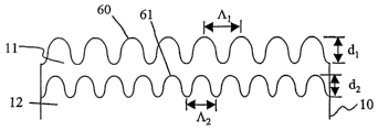
FIG. 6 is another cross-sectional view of one side a holographic media of a
fourth
embodiment of the present invention having an internal surface and an external
surface
both patterned with,an ARS surface;
FIG. 7A is an example of a patterned ARS surface of triangular structures
which
may be used in the holographic media of the embodiments of FIGS. 3-6;
FIG. 7B is an example of a patterned ARS surface of staircase structures which
may
be used in the holographic media of the embodiments of FIGS. 3-6;
FIG. 7C is an example of a patterned ARS surface of pyramidal structures which
may be used in the holographic media of the embodiments of FIGS. 3-6;
FIGS. 8A, 8B, and 8C are further examples of ARS surfaces that contain more
than
one series of periodic structured surfaces (FIG. 8A), surfaces in which the
periodicity of the
structure spans numerous surface-relief features (FIG. 8B), and surfaces that
contain
random structures (FIG. 8C), which may be used in the holographic media of the
embodiments of FIGS. 3-6;
FIG. 9 is an example of an ARS surface having structures comprising of a
periodic
2-D array of binary features, which may be used in the holographic media of
the
embodiments of FIGS. 3-6; and
CA 02545927 2006-05-12
WO 2005/050627 PCT/US2004/038020
FIG. 10 is a graph of reflectivity versus angle of incidence (AOIJ for TE and
TM
polarized illumination at a wavelength of 532nm off of a 2-D binary ARS
surface, such as
shown in FIG. 9.
Detailed Description of the Invention
Referring to FIGS. 3-6, different embodiments of the present invention are
shown for
applying structures to surfaces of holographic data storage media. In these
figures, and other
following figures showing surfaces with ARS structures, the scale of the
structures has been
exaggerated for purposes of illustration. The holographic media with such
structured surfaces
may be used in holographic data storage systems (HDSS). Such an HDSS is shown,
for
example, in U.S. Patent No. 5,621,549. The ARS surfaces are applicable to
holographic media
which may be in disk, card, coupon or other media shape or volume formats. As
such, these
figures only depict cross-sectional views along one side of the media. The
structured surfaces
of the media are one- or two-dimensional, and have a depth into the surface
along a third
dimension. The structured surfaces presenting ARS surfaces have subwavelength
surface
features having anti-reflection optical properties. Such ARS surfaces
represent surface-relief
gratings, that impedance match the material upon which they are formed with
another, such as
a gas (or air) when the ARS surface is an external surface of the media, or a
solid for an
internal surface in the media. By structuring a surface with a subwavelength-
period pattern
(either through etching, embossing, or other techniques), an effective index
of refraction
distribution is synthesized so that surface reflections are minimized. The ARS
surface is
optimized for a media for use in accordance with the operating optical
parameters of the HDSS
to use the media for storing holographic data. Such optical parameters
include, for example,
wavelengths) of operation (spectral bandwidth), range of angle of incidence
(angular
bandwidth), and polarization of incident light by such object and reference
beams of the HDSS.
Depending on such operating parameters of wavelengths) and range of angle of
incident, the
ARS structures may operate over large spectral bandwidth and fields of view.
FIG. 3 shows a first embodiment of holographic media 10 in which an ARS
surface 30
is applied to an external surface of the holographic media 10 such that it is
placed on top of the
substrate 11 adjoining or encapsulating the photosensitive material 12 of the
media. The
substrate 11 may be of glass, or plastic, such as polycarbonate or other
polymer materials. For
example, the substrate may be 0.6mm thick, and the photosensitive material
O.Smm thick. This
ARS surface 30 is fabricated from a material 31 that is different from the
substrate 1 l, but
preferentially has an index of refraction that approximately matches in order
to minimize
reflections at that surface.
CA 02545927 2006-05-12
WO 2005/050627 PCT/US2004/038020
_g_
The structures of the ARS surface may be on other external surfaces as shown
in FIGS.
4 and 5. FIG. 4 shows a second embodiment of holographic media 10 in which an
ARS
surface 30 is applied directly into the substrate 11 that adjoins
photosensitive material 12 of the
media. FIG. 5 shows a third embodiment of holographic media 10 in which the
ARS surface is
applied directly (or patterned) into the photosensitive material 12. For
example, moldable
chalcogenide material, such as that developed by Polight (Polight Technologies
Ltd.,
Cambridge, England), may be used in this embodiment to form the ARS surface,
see also
Aitken et. al., United States Patent Application No. 200410079114, published
April 29, 2004,
or U.S. Patent Application No. 101283,402, filed October 29, 2002, entitled
"Low-Temperature
Fabrication of Glass Optical Components". In another example, LiNb03 or other
photorefractive materials suitable for holographic recording can be patterned
with ARS
surfaces, via photolithographic and etching processes. However other
photopolymer materials
capable of being patterned with an ARS surface may also be used. The ARS
surfaces 30 of
media 10 of FIGS. 3-5 may be achieved by having structures with a lateral
dimension, A, that is
smaller than the operation wavelengths) of the HDSS, and in general the depth
d is smaller or
on the order of the incident wavelength.
The ARS structures may be applied to both an external surface, as well as an
internal
surface of the holographic media 10. For example, FIG. 6 shows a fourth
embodiment of
holographic media 10 in which an ARS surface is provided on an external
surface 60 on
substrate 11, and another ARS surface is provided on an internal surface 61 on
the
photosensitive material 12 of the media. The grating period A1 and depth dl of
the ARS
features of the external surface 60 need not match those (AZ and d2,
respectively) of the ARS
features of the internal surface 61. The ARS surfaces of FIG. 6 may be
achieved by having
structures with orthogonal dimensions A1 and A2 that are smaller than the
operation
wavelengths) of the HDSS, and in general the depth d is smaller or on the
order of the incident
wavelength.
As an illustrative example of the holographic media 10 of the fourth
embodiment,
consider the case in which the media has a photosensitive material suitable
for holographic
recording is to be encapsulated with another material. If the index of
refraction of the
photosensitive material is different from the material encapsulating it, light
will reflect off of
this boundary. To suppress such reflections, this fourth embodiment covers the
case in which
one or more of the internal surfaces (such as the boundaries between two
materials) are
patterned with an ARS to suppress reflections inside of the holographic media.
In FIGS. 3-6 only one side of the holographic media is shown and the sides are
illustrated as being essentially flat. This invention is not restricted to
such planar embodiments
CA 02545927 2006-05-12
WO 2005/050627 PCT/US2004/038020
_g_
of holographic media, but applies to other forms, such as, cubical, spherical,
and cylindrical.
Further, on any of the other sides of a holographic media, there is another
ARS surface (or no
ARS surface) that may have the same or different structures from the ARS
surface of the first
side.
Although structures with approximately sinusoidal cross-sections for the ARS
surface
are shown in FIGS. 3-6, such structures may be sinusoidal-like structures
which are not
actually sinusoidal in shape, or may be of other periodic profiles than
sinusoidal or sinusoidal-
like. For example, the ARS surface may have structures having profiles that
are triangular as
shown in FIG. 7A, staircase as shown in FIG. 7B, pyramidal as shown in FIG.
7C, or lamellar.
Similarly, like structures which are not actually triangular, staircase,
pyramidal, or lamellar
may also be used. Further, the steps of the staircase stl-ucture although
shown in FIG. 7B as
having equal step sizes may have different step sizes. These profiles, for
example, can be 1-D
(e.g., FIG. 7A) or 2-D (e.g., FIG. 7C) regular profiles or can be 1-D or 2-D
random or pseudo
random profiles that exhibit AR properties at the operating wavelength of the
HDSS. Although
these profiles are described as 1-D or 2-D, they have depth which provides a 3-
D profile. Also,
although a single material 11 is depicted as separating the photosensitive
material 12 and the
material containing the ARS surface 31, any number of materials can separate
the two, which
can have an ARS surface. For 2-D structures, the feature dimensions (period)
A1 and AZ may
be the same or different in each dimension.
Different methods of fabricating the ARS surfaces of media 10 may be used, all
of
which require first fabricating a patterned surface in a suitable material.
Once a substrate
material has been selected and a substrate with said material has been
obtained, the surface of
such substrate can be patterned using processes that include coating the
substrate with
photoresist and then performing photolithography, holography, laser writing,
or e-beam
lithography to pattern the photoresist layer. Such processes, for example, are
described in
Micro-Optics: Elements, Systems, and Applications, ed. by H. P. Herzig (Taylor
& Francis,
Inc. Bristol, PA, 1997). The photoresist can be etched-transferred into the
underlying substrate,
via etching methods as aqueous chemical etching or dry etching processes, such
as ion milling,
reactive ion etching, chemically assisted ion beam etching, or reactive ion
beam etching. The
remaining photoresist is removed from the surface and additional photoresist
and etching steps
can be conducted if required to achieve the final structure. The etched
structure can serve as
the final product, if the substrate material initially selected is the
photosensitive material or one
of the substrate materials encapsulating the photosensitive material. The
preferred embodiment
is to use the etched substrate material as part of the process required to
form a mold tool with
which to replicate the required surface onto the portion of the holographic
media required. For
CA 02545927 2006-05-12
WO 2005/050627 PCT/US2004/038020
-10-
example, the etched substrate can be used as the mold tool directly or the
etched substrate can
be used to form the mold tooling by nickel electroforming. If the mold tooling
is to be
fabricated via an electroforming process, such tooling may also be fabricated
directly from a
photoresist pattern and can bypass the etching process described earlier. Once
a suitable mold
tool is created, its surface may be treated with a chemical or material that
will act as a release
agent during the molding process. Depending upon the material being molded,
replication
techniques that can be used to create the final ARS surface include, by way of
example, hot
embossing, injection molding, compression molding, compression injection
molding, and cast-
and-cure. A replicated material may also be used (for example, a polymer
material) with an
ARS surface on another substrate as an etch mask. The replicated surface can
then be
transferred into the underlying surface via etching.
Although the ARS surfaces, may be patterned or etched, the preferred method
for
fabricating ARS surfaces is through a low-cost method of replication, and in
particular using a
polymer material through a cast-and-cure method, wherein the polymer film is
cast with the
required structure that exhibits anti-reflection properties onto one or more
of the external
surfaces of a holographic media. The polymer material is preferably ideally
index-matched to
the material it is replicated onto so that there is minimal reflection at that
interface. Other
methods of forming structured surfaces of the media 10 along one or more of
its external
surfaces may be by direct molding (by way of example, hot embossing, injection
molding, or
compression injection molding).
When one or more of the external surfaces of the holographic media is a
polymer
surface, the surface may be molded with the required ARS surface.
Polycarbonate (PC) is one
example of a suitable polymeric material, since PC disks are fabricated in
volumes of hundreds
of millions per year for CDs and DVDs and are already molded with the pit and
groove
structure required for these storage devices. PC disks, coupons, or other
shaped media suitable
for an HDSS can be molded with the ARS surface. Other suitable polymeric
materials that are
also available and can be used for substrates include, by way of example but
are not limited to,
cyclic olefin copolymers, such as Zeon Zeonur 10208 or Ticona Topas 5013,
acrylates, such as
Acrylic VOD (Atofina, now called Arkema Group, France), and methacrylates,
such as .
polymethylmethacrylate (PMMA). For holographic disk media that uses
photopolymerizable
materials) as the recording media, the bounding substrates of the media can be
PC or other
suitable polymeric substrates with molded ARS surfaces. This is particularly
advantageous in
that the AR coating for the surface does not require a separate step but can
be accomplished
when the disk itself is molded. Also, AR coatings using thin films tend to be
problematic if
CA 02545927 2006-05-12
WO 2005/050627 PCT/US2004/038020
-11-
they are required to operate over a broad angular range on PC or other
polymeric substrate
materials, since plastic is more difficult to coat then glass or other
substrate materials.
The methods and processes described in the previous paragraph can be used to
fabricate
a variety of ARS surfaces for holographic data storage applications. For
example, ARS
surfaces may be molded directly in polycarbonate or other suitable polymer
substrate material
of holographic media 10 of FIGS. 3, 4, and 6, or patterned on the surface of
LiNb03 or other
photosensitive (photorefractive) material suitable for holographic data
storage of FIGS. 5 and
6, or molded on the surface of a chalcogenide glass substrate that is used for
holographic data
storage. The methods and process described in the previous paragraph can be
used to achieve a
variety of surface-relief structures.
FIGS. 8A-8C show other ARS surfaces having different profiles. FIG. 8A depicts
an
ARS surface that contains a collection of more than one structure type. As
depicted, the
surface contains two periodic sets of periodic structures, one triangular
surface structure 80
with period A3 and depth d3, and one stair-stepped surface structure 81 with
period A4 and
depth d4. The depicted surface is an illustrative example and in general a
plurality of periodic
structures can be fabricated and the mix of periodic structures can occur in
one or more
dimensions across the surface. For example, if x and y are orthogonal axes
along a surface, a
profile may be periodic along the x or y axis, or along both the x and y axes,
or in combination
with another axis, such as in a hexagonal array structure which may be
periodic in three
directions along a surface. FIG. 8B depicts an ARS surface 82 in which
multiple features are
present within one region of periodicity. As depicted, there are four
structures within one
region of periodicity A4. In two dimensions areas of periodicity can be
constructed in which
multiple features lie within them. FIG. 8C depicts an ARS surface in which the
surface has
random structures. The randomness of the structure can be achieved via a
variety of process,
such as holographic recording of laser speckle, or by an etching process that
selectively etches
one or more components from a multi-component material. Preferably, the random
structure
has a correlation length of the surface randomness shorter than the
wavelengths) of HDSS
operation, such that scattering from the random structure is minimized.
FIG. 9 shows an example of a 2-D binary ARS profile that is patterned on one
of the
materials 81 of a holographic media. The ARS has binary features 80 that have
a periodicity of
AX and Ay in the x and y directions, respectively.
An ARS surface is designed by preferentially setting the grating period of the
structure
such that no orders propagate in the holographic media other than the zeroth
order according to
CA 02545927 2006-05-12
WO 2005/050627 PCT/US2004/038020
-12-
A < ~ , (1)
ray + h.i sin Bl
where ~, is the free-space wavelength, A is the grating period, n; and nt are
the indices of
refraction of the incident and transmitting media, respectively, and 8; is the
angle of incidence
in the incident medium as measured with respect to the surface normal of the
boundary
between the two materials. ARS surfaces with 2-D profiles, e.g., cross
gratings and moth eye
structures, are preferential when the HDSS requires low reflectivity for both
TE and TM
polarizations. For the specific case of an ARS with a binary structure, one
starts the vector
diffraction design, such as described in M. G. Moharam and T. K. Gaylord,
"Diffraction
analysis of dielectric surface-relief gratings," J. Opt. Soc. Am. 72, 1385-
1392 (1982), using a
seed depth d of
d = ~' , (2)
4 n~ ~t
For 2D profiles that are continuous in profile, see E. B. Grann, M. G.
Moharam, and D. A.
Pommet, "Optimal design for antireflective tapered two-dimensional
subwavelength grating
structures," J. Opt. Soc. Am. A 12(2), 333-339 (1995).
As an example of an ARS surface, consider a HDSS operating at 532 nm. Consider
also that this HDSS operates with holographic media that is comprised of two
polycarbonate
(n = 1.59) substrates that sandwich a holographic material. Further, consider
that a binary 2-D
ARS surface is desired having air-to-polycarbonate reflections are suppressed
for TE and TM
polarizations from normal incidence to an angle of incidence in air of about
50°. Using vector
diffraction model one obtains the reflectivity performance versus angle of
incidence (AOI) in
air depicted in FIG. 10 for the ARS surface profile parameters of AX = Ay =
0.200 ~.m,
d = 0.127 Vim, and aX/AX = ay/AY =50%, where AX and Ay is the grating period
in the x and y
dimensions, respectively, and ax and ay is the amplitude (or width) of each
structure in the x
and y dimensions, respectively, and d is the depth of the structures, as
illustrated for example in
FIG. 9. For example, such an ARS surface can be molded into the polycarbonate
surface
directly when the substrate itself is molded. In comparison, the reflectivity
of a bare
polycarbonate surface in air will reflect TE-polarized light with a
reflectivity of 5.2% at normal
incidence to a 20.7% reflectivity at 60°.
For the case of structure surfaces for the application of increasing adhesion
between
two or more materials within a holographic media, any of the structures shown
in FIGS. 7A-C,
8A-C, and 9 can be used. Any of these structures, be they 1-D, 2-D, periodic,
and or random,
have a larger surface area than an unpatterned surface. Therefore, by
increasing the surface
area of the interface between the two materials, one increases the bond
between said two
CA 02545927 2006-05-12
WO 2005/050627 PCT/US2004/038020
-13-
materials. For example, such adhesion promotion structures may be along an
interfacing
surface (e.g., surface 61 of FIG. 6) between photosensitive material 12 and
substrate 11
adjoining the photosensitive material. If the two materials have indices of
refraction that are
similar (e.g., within 0.06), then the surface structures required for adhesion
promotion do not
require sub-wavelength features, but instead can be features that are
significantly larger than
the wavelength of operation of the HDSS, and therefore easier to manufacture.
For the case of
two materials within a holographic media that require good adhesion and which
have indices of
refraction of sufficient difference as to require some means of suppressing
Fresnel reflections,
the ARS surfaces described in FIGS. 3-9 can serve this dual purpose of
suppressing Fresnel
reflections and adhesion promotion.
The surface structures and the fabrication methods described earlier are
examples of
structures that can be designed for AR applications and/or adhesion promotion
applications,
and methods in which a surface can be patterned with structures that are on
the order of or
smaller than the wavelength of application. Other methods of fabricating the
structured
surfaces may be used depending the material the structured surface is to be
applied to,
specifications for the structure in accordance with the operational parameters
of the HDSS, or
the environmental requirements for such a structure (e.g., temperature
sensitivity). Thus,
different surface-relief structures can be designed that exhibit AR
characteristics and/or
promote adhesion.
Although the ARS surfaces are described as alternatives to the use of AR
coatings on
the media, when such structured surfaces are used along an interior surface of
the media with
or without an ARS surface for reducing reflectivity, AR coatings may also be
applied upon the
media.
From the foregoing description it will be apparent that there has been
provided
holographic data storage media having one or more structured surfaces, and
methods for
providing such media. The illustrated description as a whole is to be taken as
illustrative and
not as limiting of the scope of the invention. Such variations, modifications
and extensions,
which are within the scope of the invention, will undoubtedly become apparent
to those skilled
in the art.