Note: Descriptions are shown in the official language in which they were submitted.
CA 02546197 2006-05-16
1
DESCRIPTION
OPTICAL SIGNAL PROCESSING METHOD AND DEVICE
TECHNICAL FIELD
[0001 ] The present invention relates to an optical signal processing
method and an optical signal processing device, a nonlinear optical loop
mirror and a designing method thereof, and an optical signal conversion
method, for use in, for example, optical fiber communication systems and for
use in an optical analog-to-digital conversion method and device for
converting an optical analog signal into an optical digital signal.
BACKGROUND ART
[0002] Conventionally, analog-to-digital conversion (referred to as A/D
conversion hereinafter) has been realized through the digitizing, quantization
and encoding processings, and these processings have been conventionally
performed through the electrical signal processings using semiconductor
devices.
[0003] Currently, there is a demand for analog-to-digital conversion
processing by the high-speed optical processing. For example, non-patent
documents 1 and 2 (referred to as prior art examples hereinafter) disclose a
method of quantizing an optical analog signal using a Mach-Zehnder
interferometer type optical modulator as a sample hold circuit, performing
photoelectric conversion using a photo-detector, and encoding a converted
electric signal using electric circuits.
[0004] Patent Document 1: Japanese patent laid-open publication No.
PO 1-271730A.
Patent Document 2: Japanese patent laid-open publication No. P2000-
010129A.
Patent Document 3: Japanese patent laid-open publication No. P9-
033967A.
Patent Document 4: Japanese patent laid-open publication No. P9-
222620A.
CA 02546197 2006-05-16
2
Patent Document 5: Japanese patent laid-open publication No. P9-
10299 lA.
Patent Document 6: Japanese patent laid-open publication No. P2000-
321606A.
Patent Document 7: Japanese patent laid-open publication No. P2001-
117125A.
Patent Document 8: Japanese patent laid-open publication No. P8-
146473A.
Patent Document 9: Japanese patent laid-open publication No. P2002-
525647A.
Patent Document 10: Japanese patent laid-open publication No.
P2003-10754 lA.
Non-Patent Document 1: Henry F. Taylor, "An Optical Analog-to-digital
Converter-Design and Analysis", IEEE Journal of Quantum Electronics, Vol.
QE-15, No. 4, April 1979.
Non-Patent Document 2: B. Jalali et al., "Optical folding-flash analog-
to-digital converter with analog encoding", Optical Letters, Optical Society
of
America, Vol. 20, No. 18, September 15, 1995.
Non-Patent Document 3: N. J. Doran et al., "Nonlinear-optical loop
mirror", Optical Letters, Optical Society of America, Vol. 13, No. 1, January
1988.
Non-Patent Document 4: Takashi Yamamoto et al., "Demultiplexing of
Sub-Tera-bit TDM optical signal with a super high-speed nonlinear optical
loop mirror", Technical Report of the Institute of Electronics Information and
Communication Engineers, C-I, issued from the Institute of Electronics
Information and Communication Engineers, Vol. J82-C-1, pp. 109-116,
March 1999.
Non-Patent Document 5: Govind P. Agrawal, "NONLINEAR FIBER
OPTICS", Academic Press, ISBN: 0120451433, 3rd Edition, pp. 210-211,
January 15, 2001.
CA 02546197 2006-05-16
3
Non-Patent Document 6: Stephen M. Jensen, "The Nonlinear Coherent
Coupler", IEEE Journal of Quantum Electrics, Vol. QE-18, No. 10, October
1982.
Non-Patent Document 7: William S. Wong et al., "Self-switching of
optical pulses in dispersion-unbalanced nonlinear loop mirrors", Optics
Letters, Optical Society of America, Vol. 22, pp. 1150-1152, 1997.
Non-Patent Document 8: I. Y. Khrushchev et al., "High-quality laser
diode pulse compression in dispersion-imbalanced loop mirror", Electronics
Letters, Vol. 34, pp. 1009-1010, May 1998.
Non-Patent Document 9: K. R. Tamura et al., "Spectral-Smoothing and
Pedestal Reduction of Wavelength Tunable Quasi-Adiabatically Compressed
Femtosecond Solitons Using a Dispersion-Flattened Dispersion-Imbalanced
Loop Mirror", IEEE Photonics Technology Letters, Vol. 11, pp. 230-232,
February 1999.
Non-Patent Document 10: K. J. Blow et al., "Demonstration of the
nonlinear fiber loop mirror as an ultrafast all-optical demultiplexer",
Electronics Letters, Vol. 26, pp. 962-964, 1990.
DISCLOSURE OF INVENTION
PROBLEMS TO BE SOLVED BY THE INVENTION
[0005] In the above mentioned prior art examples, the electric circuits
are employed as encoding circuits. Accordingly, there is a limit due to the
response speed of the semiconductor device, and therefore, it is impossible
to perform processing at a high speed such as an order of THz,
[0006] In addition, although the patent document 1 discloses an optical
A/D conversion device using a nonlinear Fabry-Perot resonator, the optical
A/D conversion device only converts the optical analog signal into the binary
optical digital signal, and the patent document 1 does not disclose any
optical circuit for encoding.
[0007] Namely, there has been such a problem in the prior art that an
optical analog-to-digital converter has not been developed and practically
CA 02546197 2006-05-16
4
used for converting the optical analog signal into the optical digital signal,
which is capable of performing the encoding and quantization processings on
the optical signal, and capable of performing the high-speed processing at a
frequency of an order of THz or higher.
[0008] An object of the present invention is to provide a method and a
device for optical signal processing for use in a method and a device for
optical A/D conversion, which are capable of solving the above-mentioned
problems, encoding and quantization processings on an optical signal, and
performing a high-speed processing at a frequency of an order of THz or
higher, while having a simple configuration.
(0009] In addition, another object of the present invention is to provide
a method and a device for optical signal processing, a nonlinear optical loop
mirror, and a designing method thereof and an optical signal conversion
method for use in, for example, optical fiber communication systems and for
use for a method and a device for optical analog-to-digital conversion for
converting an optical analog signal into an optical digital signal.
MEANS FOR SOLVING THE PROBLEMS
[0010] According to the first aspect of the present invention, there is
provided an optical signal processing method including the steps of
performing predetermined signal processing on a pulse train of signal light
having a first wavelength according to control light having a pulse train
having a second wavelength different from the first wavelength, by using an
optical signal processor including an optical nonlinear device having an
input-to-output characteristic with predetermined periodicity with respect to
light intensity, and outputting a resultant signal light.
[0011] According to the second aspect of the present invention, there is
provided an optical signal processing method including the steps of
performing predetermined optical logic operation processing on a pulse train
of signal light having a first wavelength, by making use of one of (a) a
plurality of control lights each having a pulse train having a second
CA 02546197 2006-05-16
wavelength different from the first wavelength and (b) control light having a
pulse train having a plurality of wavelengths different from the first
wavelength, by using an optical signal processor including an optical
nonlinear device having an input-to-output characteristic with periodicity
5 corresponding to a predetermined optical logic operation with respect to
light
intensity, and outputting a resultant signal light.
[0012] In the above mentioned optical signal processing method, the
optical encoder preferably includes a first optical nonlinear device anal has
a
first input end for inputting the pulse train of the signal light, a second
input
end for inputting the pulse train of the control light, and an output end for
outputting a pulse train of optically-encoded signal light.
[0013] According to the third aspect of the present invention, there is
provided an optical signal processing method including the steps of optically
encoding a pulse train of signal light having a first wavelength according to
control light which has a second wavelength different from the first
wavelength and a pulse train of an optically sampled optical analog signal,
by using a plurality of optical encoders each of which includes optical
nonlinear devices having input-to-output characteristics with different
periodicities with respect to light intensity, respectively, and outputting a
plurality of pulse trains of optically-encoded signal light from the
respective
optical encoders.
[0014] In the above mentioned optical signal processing method, the
optical encoders are preferably "N" optical encoders each having an input-to-
output characteristic with a period of T/2~N-~1, where "N" is a natural number
(N = 1, 2, 3...) indicating a quantifying bit number.
[0015] According to the fourth aspect of the present invention, there is
provided an optical signal processing method including the steps of decoding
a pulse train of a multi-level optical signal having a first wavelength into a
plurality of binary optical signals according to control light having a pulse
train having a second wavelength different from the first wavelength, by
CA 02546197 2006-05-16
6
using a plurality of optical signal processors including optical nonlinear
devices having input-to-output characteristics with different periodicities
with respect to light intensity, and outputting the binary optical signals.
[0015] In the above mentioned optical signal processing method, each
of the optical encoders preferably includes a first optical nonlinear device
and has a first input end for inputting the pulse train of the signal light, a
second input end for inputting the pulse train of the control light, and an
output end for outputting a pulse train of optically-encoded signal light.
[0017] In addition, in the above mentioned optical signal processing
method, the first optical nonlinear device is preferably a nonlinear optical
loop mirror. In the other case, the first optical nonlinear device is
preferably
a Kerr shutter which utilizes an optical Kerr effect of a nonlinear optical
effect. Instead, the first optical nonlinear device is preferably a waveguide-
type Mach-Zehnder interferometer.
[0018] According to the fifth aspect of the present invention, there is
provided an optical signal processing device including signal processing
means for performing predetermined signal processing on a pulse train of
signal light having a first wavelength according to control light having a
pulse train having a second wavelength different from the first wavelength,
by using an optical signal processor including an optical nonlinear device
having an input-to-output characteristic with predetermined periodicity with
respect to light intensity, and for outputting a resultant signal light.
[0019] According to the sixth aspect of the present invention, there is
provided an optical signal processing device including operating means for
performing predetermined optical logic operation processing on a pulse train
of signal light having a first wavelength, by making use of one of (a} a
plurality of control lights each having a pulse train having a second
wavelength different from the first wavelength and (b) control light having a
pulse train having a plurality of wavelengths different from the first
wavelength, by using an optical signal processor including an optical
CA 02546197 2006-05-16
nonlinear device having an input-to-output characteristic with periodicity
corresponding to a predetermined optical logic operation with respect to light
intensity, and for outputting a resultant signal light.
[0020] In the above mentioned optical signal processing device, the
optical encoder preferably includes a first optical nonlinear device and has a
first input end for inputting the pulse train of the signal light, a second
input
end for inputting the pulse train of the control light, and an output end for
outputting a pulse train of optically-encoded signal light.
[0021] According to the seventh aspect of the present invention, there is
provided an optical signal processing device including optical encoding
means for optically encoding a pulse train of signal light having a first
wavelength according to control light which has a second wavelength
different from the first wavelength and a pulse train of an optically sampled
optical analog signal, by using a plurality of optical encoders each of which
includes optical nonlinear devices having input-to-output characteristics
with different periodicities with respect to light intensity, respectively,
and
far outputting a plurality of pulse trains of optically-encoded signal light
from the respective optical encoders.
[0022] In the above mentioned optical signal processing device, the
optical encoders are preferably "N" optical encoders each having an input-to-
output characteristic with a period of T/2~N-l~, where "N" is a natural number
(N = 1, 2, 3...) indicating a quantifying bit number.
[0023] According to the eighth aspect of the present invention, there is
provided an optical signal processing device including mufti-level decoding
means for decoding a pulse train of a mufti-level optical signal having a
first
wavelength into a plurality of binary optical signals according to control
light
having a pulse train having a second wavelength different from the first
wavelength, by using a plurality of optical signal processors including
optical
nonlinear devices having input-to-output characteristics with different
periodicities with respect to light intensity, and for outputting the binary
CA 02546197 2006-05-16
8
optical signals.
[0024) In the above mentioned optical signal processing method, each
of the optical encoders preferably includes a first optical nonlinear device
and has a first input end far inputting the pulse train of the signal light, a
second input end for inputting the pulse train of the control light, and an
output end for outputting a pulse train of optically-encoded signal light.
[0025] In addition, in the above mentioned optical signal processing
method, the first optical nonlinear device is preferably a nonlinear optical
loop mirror. In the other case, the first optical nonlinear device is
preferably
a Kerr shutter which utilizes an optical Kerr effect of a nonlinear optical
effect. Instead, the first optical nonlinear device is preferably a waveguide-
type Mach-Zehnder interferometer.
[0026] According to the ninth aspect of the present invention, there is
provided an optical signal processing method for optically analog-to-digital
converting an optically sampled optical analog signal into an optical digital
signal. The method includes an optically encoding step and an optically
quantizing step. The optically encoding step optically encodes a pulse train
of signal light having a first wavelength according to control light which has
a second wavelength different from the first wavelength and has a pulse train
of an optically sampled optical analog signal, by using a plurality of optical
encoders each including optical nonlinear devices having input-to-output
characteristics with different periodicities with respect to the light
intensity,
and outputs a plurality of pulse trains of optically-encoded signal light from
the respective optical encoders. The optically quantizing step performs
optical threshold processing on the pulse trains of optically-encoded signal
light to optically quantize the pulse trains of optically-encoded signal
light,
by using at least one of optical threshold processors each of which is
connected to each of the optical encoders and includes a nonlinear optical
device having a nonlinear input-to-output characteristic with respect to light
intensity, and outputs optically quantized pulse trains as optical digital
CA 02546197 2006-05-16
9
signals.
[0027] The above mentioned optical signal processing method
preferably further includes the steps of optically sampling an optical analog
signal at a predetermined sampling frequency, and outputting an optically
sampled optical analog signal, prior to the optically encoding step.
[0028] In addition, in the above mentioned optical signal processing
method, the optical encoders are preferably "N" optical encoders each having
an input-to-output characteristic with a period of T/2~N-z~, where "N" is a
natural number (N ~ 1, 2, 3...] indicating a quantifying bit number.
[0029] Further, in the above mentioned optical signal processing
method, the optically encoding step preferably includes a step of optically
quantizing each of the pulse trains of optically-encoded signal light, by
using
one of a single optical threshold processor and a plurality of optical
threshold processors connected in cascade to each other for optically
quantizing a pulse train of inputted signal light.
[0030] Still further, in the above mentioned optical signal processing
method, each of the optical encoders preferably includes a first optical
nonlinear device and has a first input end for inputting the pulse train of
the
signal light, a second input end for inputting the pulse train of the control
light, and an output end for outputting a pulse train of optically-encoded
signal light.
[0031] In addition, in the above mentioned optical signal processing
method, each of the optical threshold processors preferably includes a
second optical nonlinear device and has a first input end for inputting one of
continuous light of predetermined carrier wave light and a pulse train of the
predetermined carrier wave light, a second input end for inputting the pulse
train of optically encoded signal light, and an output end for outputting the
optically-quantized pulse train.
[0032] Further, in the above mentioned optical signal processing
method, each of the optical threshold processors preferably includes a
CA 02546197 2006-05-16
second optical nonlinear device and has an input end for inputting one of
continuous light of predetermined carrier wave light and a pulse train of the
predetermined carrier wave light, and an output end for outputting the
optically-quantized pulse train. .
5 [0033] Still further, in the above mentioned optical signal processing
method, the first optical nonlinear device is preferably a nonlinear optical
loop mirror. In the other case, the first optical nonlinear device is
preferably
a Kerr shutter which utilizes an optical Kerr effect of a nonlinear optical
effect. Instead, the first optical nonlinear device is preferably a waveguide-
10 type Mach-Zehnder interferometer.
[0034] Still further, in the above mentioned optical signal processing
method, the second optical nonlinear device is preferably a nonlinear optical
loop mirror. In the other case, the second optical nonlinear device is
preferably a Kerr shutter which utilizes an optical Kerr effect of a nonlinear
optical effect. Instead, the second optical nonlinear device is preferably a
waveguide-type Mach-Zehnder interferometer.
[0035] According to the tenth aspect of the present invention, there is
provided an optical signal processing device for optically analog-to-digital-
converting an optically sampled optical analog signal into an optical digital
signal. The device includes optically encoding means and optically
quantizing means. The optically encoding means optically encodes a pulse
train of signal light having a first wavelength according to control light
which
has a second wavelength different from the first wavelength and has a pulse
train of an optically sampled optical analog signal, by using a plurality of
optical encoders each including optical nonlinear devices having input-to-
output characteristics with different periodicities with respect to the light
intensity, and outputs a plurality of pulse trains of optically-encoded signal
light from the respective optical encoders. The optically quantizing means
performs optical threshold processing on the pulse trains of optically-
encoded signal light to optically quantize the pulse trains of optically-
CA 02546197 2006-05-16
11
encoded signal Iight, by using at least one of optical threshold processors
each of which is connected to each of the optical encoders and includes a
nonlinear optical device having a nonlinear input-to-output characteristic
with respect to light intensity, and outputs optically quantized pulse trains
as optical digital signals.
[0036] The above mentioned optical signal processing device preferably
further includes optically sampling means for optically sampling an optical
analog signal at a predetermined sampling frequency, and for outputting an
optically sampled optical analog signal, at the previous stage of the
optically
encoding means.
(0037] In addition, in the above mentioned optical signal processing
device, the optical encoders are preferably "N" optical encoders each having
an input-to-output characteristic with a period of TJ2~N-l~, where "N" is a
natural number (N = 1, 2, 3...j indicating a quantifying bit number.
[0038] Further, in the above mentioned optical signal processing device,
the optically encoding step preferably includes a step of optically quantizing
each of the pulse trains of optically-encoded signal light, by using one of a
single optical threshold processor and a plurality of optical threshold
processors connected in cascade to each other for optically quantizing a
pulse train of inputted signal light.
[0039] Still further, in the above mentioned optical signal processing
device, each of the optical encoders preferably includes a first optical
nonlinear device and has a first input end for inputting the pulse train of
the
signal light, a second input end for inputting the pulse train of the control
light, and an output end for outputting a pulse train of optically-encoded
signal light.
(0040] In addition, in the above mentioned optical signal processing
device, each of the optical threshold processors preferably includes a second
optical nonlinear device and has a first input end for inputting one of
continuous light of predetermined carrier wave light and a pulse train of the
CA 02546197 2006-05-16
12
predetermined carrier wave light, a second input end for inputting the pulse
train of optically encoded signal light, and an output end for outputting the
optically-quantized pulse train.
[0041] Further, in the above mentioned optical signal processing device,
each of the optical threshold processors preferably includes a second optical
nonlinear device and has an input end for inputting one of continuous light
of predetermined carrier wave light and a pulse train of the predetermined
carrier wave light, and an output end for outputting the optically-quantized
pulse train.
[0042] Still further, in the above mentioned optical signal processing
device, the first optical nonlinear device is preferably a nonlinear optical
loop
mirror. In the other case, the first optical nonlinear device is preferably a
Kerr shutter which utilizes an optical Kerr effect of a nonlinear optical
effect.
Instead, the first optical nonlinear device is preferably a waveguide-type
Mach-Zehnder interferometer.
[0043] Still further, in the above mentioned optical signal processing
device, the second optical nonlinear device is preferably a nonlinear optical
loop mirror. In the other case, the second optical nonlinear device is
preferably a Kerr shutter which utilizes an optical Kerr effect of a nonlinear
optical effect. Instead, the second optical nonlinear device is preferably a
waveguide-type Mach-Zehnder interferometer.
[0044] According to the eleventh aspect of the present invention, there
is provided a nonlinear optical loop mirror including an optical fiber, a
photo-coupler, control-light input means for inputting a control light signal
to the optical fiber, and a nonlinear medium placed on an optical path of the
optical fiber. The photo-coupler is connected so as to branch an input
optical signal inputted from an optical-signal input end into two optical
signals and to output the optical signals to both ends of the optical fiber
and
connected so as to branch and output optical signals outputted from the
both ends of the optical fiber to the optical-signal input end and an optical-
CA 02546197 2006-05-16
13
signal output end, respectively. The nonlinear optical loop mirror adjusts a
phase difference between optical signals inputted to the both ends of the
optical fibers according to power of the control light signal so as to control
power of the output optical signal outputted from the optical-signal output
end. The nonlinear optical loop mirror suppresses a parametric gain caused
among the respective branched optical signals and the control light signal,
so that a ratio of the power of the output optical signal to the maximum
value thereof becomes equal to or smaller than a predetermined threshold
value when a difference between phase shifts caused to the respective
branched optical signals is set to 2n~c (where "n" is an integer equal to or
larger than 1i, where the phase shifts are caused by cross-phase modulation
(XPM) generated among the respective branched optical signals and the
control light signal.
[0045] In the above mentioned nonlinear optical loop mirror, a
relationship of G<2Tth+ 1 is preferably set to be satisfied, where "G" is a
ratio
of amplification of the optical signal propagating in the same direction as
that of the control light signal, where the amplification is caused by the
parametric gain, and "Tth" is a ratio of the predetermined threshold value to
the maximum value of the output optical signal.
(0046] In addition, in the above mentioned nonlinear optical loop mirror,
one of the input optical signal and the control light signal is preferably
inputted after passing through an optical delay line, so that pulses of the
optical signals and pulses of the control light signal are superimposed on
each other over a predetermined range of the nonlinear medium.
[004?] Further, in the above mentioned nonlinear optical loop mirror,
polarization states of the optical signals and the control light signal are
preferably substantially identical to each other in the optical fiber and the
nonlinear medium.
[0048] Still further, in the above mentioned nonlinear optical loop
mirror, the predetermined threshold value is preferably a threshold value
CA 02546197 2006-05-16
14
required for quantiza.tion and encoding processings for optical analog-to-
digital conversion.
[0049] In addition, in the above mentioned nonlinear optical loop mirror,
the predetermined threshold value is preferably 3 dB.
[0050] Further, in the above mentioned nonlinear optical loop mirror,
one of the following conditions is preferably set to be satisfied:
(a) a dispersion value of the nonlinear medium is equal to or smaller
than the minimum dispersion value of dispersion values when the
parametric gain caused among the optical signals and the control light signal
is equal to or larger than a predetermined value; and
(b) a dispersion value of the nonlinear medium is equal to or larger
than the maximum dispersion value of dispersion values when the
parametric gain caused among the optical signals and the control light signal
is equal to or larger than a predetermined value.
[0051] Still further, in the above mentioned nonlinear optical loop
mirror, a wavelength difference between the control light signal and the
input optical signal is preferably larger than the maximum wavelength
difference which cause a parametric gain equal to or larger than a
predetermined value among the optical signals and the control light signal.
[0052] In addition, in the above mentioned nonlinear optical loop mirror,
an absolute value of a product of a wavelength difference between the control
light signal and the optical signals, and a dispersion value of the nonlinear
medium is preferably equal to or smaller than a value which suppress walk-
off and set a phase shift difference between the branched optical signals due
to cross-phase modulation (XPM) caused among the respective optical
signals and the control light signal to be equal to or larger than 2~.
[0053] Further, in the above mentioned nonlinear optical loop mirror, a
power value of the output optical signal is preferably processed as "0" in an
optical analog-to-digital conversion processing when a difference between
phase shifts caused to the respective branched optical signals is 2n~ (where
CA 02546197 2006-05-16
"n" is an integer equal to or larger than 1), where the phase shifts are
generated by cross-phase modulation (XPM) caused among the respective
branched optical signals and the control light signal.
[0054] Still further, in the above mentioned nonlinear optical loop
5 mirror, a dispersion characteristic of the nonlinear medium preferably has a
normal dispersion characteristic, at a wavelength of the control light signal.
[0055] Still further, in the above mentioned nonlinear optical loop
mirror, a dispersion characteristic of the nonlinear medium preferably has
an anomalous dispersion characteristic, at a wavelength of the control light
10 signal.
[0056] In addition, in the above mentioned nonlinear optical loop mirror,
a relationship of ~,o>~.s>~c preferably holds when a dispersion value "D" of
the
nonlinear medium differentiated with respect to a wavelength ~, is positive
(dD/d~,>0), at wavelengths of the input optical signal and the control light
15 signal.
[0057] Further, in the above mentioned nonlinear optical loop mirror, a
relationship of ~,o<~.s<7~c preferably holds when a dispersion value "D" of
the
nonlinear medium differentiated with respect to a wavelength ~, is negative
(dD/d~,<0), at wavelengths of the input optical signal and the control light
signal.
[0058] According to the twelfth aspect of the present invention, there is
provided a nonlinear optical loop mirror including an optical fiber, a photo-
coupler, control-light input means for inputting a control light signal to the
optical fiber, and a nonlinear medium placed on an optical path of the
optical fiber. The photo-coupler is connected so as to branch an input
optical signal inputted from an optical-signal input end into two optical
signals and to output the optical signals to both ends of the optical fiber
and
connected so as to branch and output optical signals outputted from the
both ends of the optical fiber to the optical-signal input end and an optical-
signal output end. The nonlinear optical loop mirror adjusts a phase
CA 02546197 2006-05-16
16
difference between optical signals inputted to the both ends of the optical
fibers according to power of the control light signal so as to control power
of
the output optical signal outputted from the optical-signal output end. A
dispersion characteristic of the nonlinear medium has a normal dispersion
characteristic, at a wavelength of the control light signal.
[0059] In the above mentioned nonlinear optical loop mirror, one of the
following conditions is preferably set to be satisfied:
(a) a dispersion value of the nonlinear medium at a wavelength of the
control light signal is equal to or smaller than -0.62 ps/nm/km and a
wavelength difference between the input signal light and the control light is
equal to or larger than 16 nm; and
(b) a dispersion value of the nonlinear medium at a wavelength of the
control light signal is equal to or smaller than -0.315 ps/nm/km and a
wavelength difference between the input signal light and the control light is
equal to or larger than 20 nm.
[0060] In addition, in the above mentioned nonlinear optical loop mirror,
polarization states of the optical signals and the control light signal are
preferably substantially identical to each other in the optical fiber and the
nonlinear medium.
[0061] According to the thirteenth aspect of the present invention, there
is provided a nonlinear optical loop mirror including an optical fiber, a
photo-coupler, control-light input means for inputting a control light signal
to the optical fiber, and a nonlinear medium placed on an optical path of the
optical fiber. The photo-coupler is connected so as to branch an input
optical signal inputted from an optical-signal input end into two optical
signals and to output the optical signals to both ends of the optical fiber
and
connected so as to branch and output optical signals outputted from the
both ends of the optical fiber to the optical-signal input end and an optical-
signal output end. The nonlinear optical loop mirror adjusts a phase
difference between optical signals inputted to the both ends of the optical
CA 02546197 2006-05-16
17
fibers according to power of the control light signal so as to control power
of
the output optical signal outputted from the optical-signal output end. A
difference between phase shifts caused to the respective optical signals, due
to cross-phase modulation (XPM) caused between the respective optical
signals and the control light signal, is equal to or larger than 2~c.
[0062] In the above mentioned nonlinear optical loop mirror, the
nonlinear medium preferably has a normal dispersion characteristic, at a
wavelength of the control light signal.
[0063] In addition, in the above mentioned nonlinear optical loop mirror,
the nonlinear optical loop mirror preferably suppresses a parametric gain
caused among the respective branched optical signals and the control light
signal, so that a ratio of the power of the output optical signal to the
maximum value thereof becomes equal to or smaller than a threshold value
for optical analog-to-digital conversion when a difference between phase
shifts caused to the respective branched optical signals is set to 2n~c (where
"n" is an integer equal to or larger than 1), where the phase shifts are
caused
by cross-phase modulation (XPM) generated among the respective branched
optical signals and the control light signal.
[0064] Further, in the above mentioned nonlinear optical loop mirror,
polarization states of the optical signals and the control light signal are
preferably substantially identical to each other in the optical fiber and the
nonlinear medium.
[0065] According to the fourteenth aspect of the present invention,
there is provided a method for designing a nonlinear optical loop mirror
including an optical fiber, a photo-coupler, control-light input means for
inputting a control light signal to the optical fiber, and a nonlinear medium
placed on an optical path of the optical fiber. The photo-coupler is
connected so as to branch an input optical signal inputted from an optical-
signal input end into two optical signals and to output the optical signals to
both ends of the optical fiber and connected so as to branch and output
CA 02546197 2006-05-16
i8
optical signals outputted from the both ends of the optical fiber to the
optical-signal input end and an optical-signal output end. The nonlinear
optical loop mirror adjusts a phase difference between optical signals
inputted to the both ends of the optical fibers according to power of the
control light signal so as to control power of the output optical signal
outputted from the optical-signal output end. The method includes first,
second, third, fourth, and fifth steps. The first step determines a transfer
function and a period (~m~) of the transfer function, the transfer function
being expressed as a relationship of power of an input optical signal with
respect to power of an output optical signal. The second step determines a
threshold value of the output optical signal suitable far optical signal
processing. The third step provisionally determines a nonlinearity constant
and a dispersion characteristic of said nonlinear medium, and a wavelength
and a peak power of the control light signal. The fourth step judges whether
or not a phase shift reaches the period ~m~, and proceeds to the fifth step
when the phase shift reaches the period ~m~, while returns to the third step
when the phase shift does not reach the period ~~,~. The fifth step judges
whether or not a relationship of G<2Tth+ 1 is satisfied, where "G" is a ratio
of
amplification of the optical signal propagating in the same direction as that
of the control light signal, where the amplification is caused by the
parametric gain, and "Tth" is a ratio of the predetermined threshold value to
the maximum value of the output optical signal, and sets the nonlinearity
coefficient and the dispersion characteristic of the nonlinear medium and the
wavelength and the peak power of the control light signal Which have been
provisionally determined to a designing determined value when the
relationship is satisfied, while returns to the third step when the
relationship
is not satisfied.
[0066] According to the fifteenth aspect of the present invention, there
is provided an optical signal conversion method including the steps of
branching an input optical signal into two optical signals (A) and (B),
CA 02546197 2006-05-16
19
propagating the optical signal (A) in the same direction as that of a control
light signal having a different wavelength so as to cause cross-phase
modulation, and changing a phase shift difference between the optical
signals (A) and (B) periodically with respect to change in power of the
control
light signal so as to change power of output optical signal resulted from
interference between the optical signals (A) and (B). The method includes
the steps of suppressing a parametric gain caused between the optical signal
(A) and the control light signal, so that the power of the output optical
signal
when the phase shift difference is 2n~ (where "n" is an integer equal to or
larger than 1 ) is equal to or smaller than a threshold value for quantization
and encoding processings for optical analog-to-digital conversion, with
respect to the maximum value of the power of the output optical signal.
EFFECTS OF THE INVENTION
[0067] The optical signal processing method and device according to
the present invention performs predetermined signal processing on a pulse
train of signal light having a first wavelength, according to control light
having a pulse train having a second wavelength different from the first
wavelength, by using an optical signal processor including an optical
nonlinear device having predetermined periodicity in the input-to-output
characteristic with respect to the light intensity. Accordingly, it is
possible to
realize optical signal processing such as optical logic operations, optical
encoding processing and multi-level decoding processing, with a simple
configuration, and it is possible to realize speeding-up as compared with the
prior art.
[0068] In addition, with the optical signal processing method and device
according to the present invention, the sampled optical analog signal can be
optically A/D-converted into the optical digital signal, and the upper limit
of
the sampling frequency can be set to an order of several GHz to several THz
in principle. Assuming that the limit of the sampling frequency of the A j D
conversion for the electric circuit is several tens of GHz, it is possible to
CA 02546197 2006-05-16
realize speeding-up by about two orders of magnitude. In addition, since the
inputting and outputting are performed with optical signals, the optical
signal processing method and device according to the present invention are
suitably applied to the optical networks.
5 [0069] Further, a nonlinear optical loop mirror having a transfer
function as shown in Fig. 40 can be realized by making a design which is
characterized to cause the gain that signal light propagating in the same
direction as that of control light receives from parametric processing caused
by the control light in an optical fiber in the nonlinear optical loop mirror
10 according to the present invention to be suppressed to be equal to or
smaller
than a permissible value determined with respect to a set threshold value.
BRIEF DESCRIPTION OF DRAWINGS
(0070] Fig. 1 is a black diagram and a timing chart showing operation
of an optical A/ D converter 100 according to a first preferred embodiment of
15 the present invention.
Fig. 2 is a block diagram showing a detailed configuration of the
optical A/D converter 100 of Fig. 1.
Fig. 3 is a block diagram showing a detailed configuration of an optical
encoder 201 of Fig. 2.
20 Fig. 4 is a graph showing a relationship between output power of
signal light (~,1) with respect to input power of control light (~,l), showing
an
operation of an optical encoder 201 of Fig. 3.
Fig. S is graphs and a block diagram showing an exemplary operation
of an optical encoding circuit 200 of Fig. 3.
Fig. 6 is a block diagram and graphs showing a detailed configuration
and an operation of an optical threshold processor 301 of Fig. 2.
Fig. ? is a graph showing an exemplary operation of the optical
threshold processor 301 of Fig. 6.
Fig. $ is a block diagram showing detailed configurations of the optical
encoding circuit 200 and an optical quantization circuit 300 of Fig. 2.
CA 02546197 2006-05-16
21
Fig. 9 is a graph showing an exemplary operation of an optical
encoder 201 of Fig. 8.
Fig. 10 is a graph showing an exemplary operation of an optical
encoder 202 of Fig. 8.
Fig. 11 is a graph showing an exemplary operation of an optical
encoder 203 of Fig. 8.
Fig. 12 is a graph showing an exemplary operation of an optical
threshold processor 301 of Fig. 8.
Fig. 13 is a graph showing an exemplary operation of an optical
threshold processor 302 of Fig. 8.
Fig. 14 is a graph showing an exemplary operation of an optical
threshold processor 303 of Fig. 8.
Fig. 15 is a block diagram showing a detailed configuration of an
optical A/D converting device 100A according to a modified preferred
i 5 embodiment of the present invention.
Fig. 16 is a graph showing an exemplary operation of optical threshold
processors 301 and 311 of Fig. 15 which are connected in cascade to each
other.
Fig. 17 is a graph showing an exemplary operation of optical threshold
processors 302, 312 and 322 of Fig. 15 which are connected in cascade to
each other.
Fig. 18 is a graph showing an exemplary operation of optical threshold
processors 303, 313, 323 and 333 of Fig. 15 which are connected in cascade
to each other.
Fig. 19 is a block diagram showing a detailed configuration of an
experimental system according to a present preferred embodiment.
Fig. 20 is a graph showing an exemplary operation of encoding
processing in an optical encoder 201 of Fig. 19.
Fig. 21 is a graph showing an exemplary operation of encoding
processing in an optical encoder 202 of Fig. 19.
CA 02546197 2006-05-16
22
Fig. 22 is a graph showing an exemplary operation of encoding
processing in an optical encoder 203 of Fig. 19.
Fig. 23 is a graph showing a 3-bit encoded value (# 1, #2 and #3} with
respect to amplitude of input analog pulses of the control light (~.z} which
is
resulted from the encoding processing using an optical encoding circuit 200
of Fig. 19.
Fig. 24 is a diagram showing encoded 3-bit encoded values (# 1, #2 and
#3) and pulse waveforms thereof, when the amplitude of analog pulses after
processing by a single optical threshold processor is changed, in the case
where the experimental system is constructed by using ideal nonlinear
optical loop mirrors in Fig. 19.
Fig. 25 is a block diagram showing a configuration of an experimental
system for a first simulation according to the present preferred embodiment.
Fig. 26 is a graph showing peak power of pulses of the signal light (~,~)
with respect to peak power of pulses of the control light (~,2), showing
results
of the first simulation of Fig. 25.
Fig. 27 is a block diagram showing a configuration of an experimental
system for a second simulation according to the present preferred
embodiment.
Fig. 28 is a waveform diagram showing a pulse waveform of signal
power from the optical encoder 201, showing results of the second
simulation of Fig. 27.
Fig. 29 is a waveform diagram showing a pulse waveform of signal
power from the optical encoder 202, showing results of the second
simulation of Fig. 27.
Fig. 30 is a waveform diagram showing a pulse waveform of signal
power from the optical encoder 203, showing results of the second
simulation of Fig. 27.
Fig. 31 is a block diagram showing a configuration of an experimental
system for a third simulation according to the present preferred embodiment.
CA 02546197 2006-05-16
23
Fig. 32 is a waveform diagram showing a pulse waveform of signal
power from the optical encoder 201, showing results of the third simulation
of Fig. 31.
Fig. 33 is a waveform diagram showing a pulse waveform of signal
power from the optical encoder 202, showing results of the third simulation
of Fig. 3 I .
Fig. 34 is a waveform diagram showing a pulse waveform of signal
power from the optical encoder 203, showing results of the third simulation
of Fig. 3 1.
Fig. 35 is a block diagram showing a configuration of an optical
encoder using a waveguide-type Mach-Zehnder interferometer according to a
first modified preferred embodiment of the present invention.
Fig. 36 is a block diagram showing a configuration of an optical
encoder using a dispersion unbalanced-nonlinear optical loop mirror
according to a second modified preferred embodiment of the present
invention.
Fig. 37 is a block diagram showing a configuration of an optical
encoder using a Kerr shutter having an optical Kerr effect according to a
third modified preferred embodiment of the present invention.
Fig. 38 is a diagram showing a configuration of a NOLM according to a
prior art and a second preferred embodiment of the present invention.
Fig. 39 is a diagram showing a relationship between an input signal
light power and an output light power of the NOLM according to the prior art.
Fig. 40 is a diagram showing a relationship between the input light
power and the output light power of the NOLM according to the second
preferred embodiment of the present invention.
Fig. 41 is a diagram showing a relationship between a parametric gain
and a dispersion value D (~.c) of an optical fiber.
Fig. 42 is a diagram showing the relationship between the parametric
gain and the wavelength difference 0~, between the signal light and the
CA 02546197 2006-05-16
24
control light.
Fig. 43 is a diagram showing a relationship between the dispersion
value of the optical fiber and an arrangement of wavelengths of the signal
light and the control light (in the case of dD/d~,>0).
Fig. 44 is a diagram showing a relationship between the dispersion
value of the optical fiber and the arrangement of the wavelengths of the
signal light and the control light (in the case of dD/d~,<0).
Fig. 45 is a flow chart showing a procedure of designing processing of
the NOLM according to the second preferred embodiment of the present
invention.
Fig. 46 is a diagram showing one implemental example of the NOLM
according to the second preferred embodiment of the present invention.
Fig. 47 is a diagram showing results of measurement of a transfer
characteristic of the NOLM according to the present preferred embodiment.
Fig. 48 is a diagram showing a transfer function of a NOLM with a
high-nonlinear fiber (HNLF) different from that employed in Fig. 47.
Fig. 49 is a diagram showing results of measurement of a transfer
characteristic of a NOLM according to a further implemental example of the
second preferred embodiment of the present invention.
Fig. 50 is a diagram showing results of measurement of a transfer
characteristic of a NOLM according to a further other implemental example
of the second preferred embodiment of the present invention.
Fig. 51 is a block diagram showing a configuration of a multi-level
optical signal decoder 400 according to a third preferred embodiment of the
present invention.
Fig. 52 is a graph showing an output pulse intensity with respect to an
input pulse intensity of respective optical signal processors 401 and 402 of
Fig. 51.
Fig. 53 is a block diagram showing a configuration of a decoding device
for use in an optical intensity multi-level communication system using the
CA 02546197 2006-05-16
mufti-level optical signal decoder 400 of Fig. 51 according to a first
exemplary application.
Fig. 54 is a table showing an exemplary code allocation for the
decoding device of Fig. 53.
5 Fig. 55 is a block diagram showing a configuration of a decoding device
for use in an optical intensity multi-level communication system according
to a second exemplary application using the mufti-level optical signal
decoder 400 of Fig. 51.
Fig. 56 is a table showing an exemplary code allocation for the
10 decoding device of Fig. 55.
Fig. 57 is a block diagram showing a configuration of an optical logic
operation circuit 600 according to a forth preferred embodiment of the
present invention.
Fig. 58 is a graph showing an output optical pulse intensity with
15 respect to the input optical pulse intensity which is resulted from an OR
operation of the optical logic operation circuit 600 of Fig, 57.
Fig. 59 is a graph showing an output optical pulse intensity with
respect to the input optical pulse intensity which is resulted from an AND
operation of the optical logic operation circuit 600 of Fig. 57.
20 Fig. 60 is a graph showing an output optical pulse intensity with
respect to the input optical pulse intensity which is resulted from a NOT
operation of the optical logic operation circuit 600 of Fig. 57.
Fig. 61 is a graph showing an output optical pulse intensity with
respect to the input optical pulse intensity which is resulted from an EXOR
25 operation of the optical logic operation circuit 600 of Fig. 57.
Fig. 62 is a block diagram showing a configuration of a forth
experimental system according to a preferred embodiment of the present
invention.
Fig. 63 is a graph showing an average power of the output signal light
with respect to the average power of the control light, showing results of
CA 02546197 2006-05-16
26
experiments with the forth experimental system of Fig. 62.
Fig. 64 is a block diagram showing a configuration of a first portion of
a fifth experimental system according to the preferred embodiment of the
present invention.
Fig. 65 is a block diagram showing a configuration of a second portion
of the fifth experimental system according to the preferred embodiment of
the present invention.
Fig. 66 is a graph showing an average power PA of output signal light
pulses outputted from an optical encoder 201A with respect to an average
power of control light pulses inputted to the optical encoder 201A, showing
results of experiments with the fifth experimental system of Figs. 64 and 65.
Fig. 67 is a graph showing an average power Ps of the output signal
light pulses outputted from an optical encoder 202A with respect to the
average power of the control light pulses inputted to the optical encoder
202A, showing results of experiments with the fifth experimental system of
Figs. 64 and 65.
Fig. 68 is a graph showing an average power Pc of the output signal
light pulses outputted from an optical encoder 203A with respect to the
average power of the control light pulses inputted to the optical encoder
203A, showing results of experiments with the fifth experimental system of
Figs. 64 and 65.
Fig. 69 is a graph showing an average power PD of the output signal
light pulses outputted from an optical threshold processor 301A with respect
to the average power of control light pulses inputted to the optical threshold
processor 301A, showing results of experiments with the fifth experimental
system of Figs. 64 and 65.
Fig. 70 is a graph showing an average power P,, of output signal light
pulses outputted from an optical threshold processor 302A with respect to
the average power of control light pulses inputted to the optical threshold
processor 302A, showing results of experiments with the fifth experimental
CA 02546197 2006-05-16
27
system of Figs. 64 and 65.
Fig. ? 1 is a graph showing an average power PF of the output signal
light pulses outputted from the optical threshold processor 303A with
respect to the average power of the control light pulses inputted to the
optical threshold processor 303A, showing results of experiments with the
fifth experimental system of Figs. 64 and 65.
Fig. 72 is graphs showing light intensities PD, PF and PF of the optical
signals outputted from the respective optical threshold processors 301A,
302A and 303A, showing results of experiments with the fifth experimental
system of Figs. 64 and 65, in the case where the average power of the control
light pulses is 200 mW, ?00 mW and 1000 rnW.
DESCRIPTION OF NUMERICAL REFERENCES
[0071] 10 ... nonlinear optical loop mirror,
l0A ... polarization controller,
11 and 12 ... photo-couplers,
13 ... optical isolator,
14 and 14A ... optical band-pass filters,
15 ... optical delay circuit,
15A ... variable optical delay circuit,
16 ... optical isolator,
16A ... optical circulator,
17 ... optical amplifier,
18 ... optical isolator,
19 ... optical fiber cable,
19A ... polarization controller,
20 ... nonlinear optical loop mirror,
20A ... polarization controller,
20B ... optical attenuator,
21 and 22 ... photo-couplers,
23 ... optical isolator,
CA 02546197 2006-05-16
28
24 ... optical band-pass filter,
25 ... laser diode,
26 and
26A
...
optical
isolators,
27 ... optical amplifier,
28 .., optical isolator,
29 ... optical fiber cable,
30 ... sampled signal generator,
31 ... laser diode,
32 ... optical isolator,
41 .. optical sampling circuit,
,
42 ... optical isolator,
50 ... fiber ring laser,
51 and
52
...
optical
band-pass
filters,
53 ... optical modulator,
54 ... data signal generator,
55, 6 and 57 ... optical splitters,
5
61 and
62
...
fiber
ring
lasers,
63 ... optical delay circuit,
71, 2 and 73 .., photo-couplers,
7
8 i
and
82
...
optical
waveguides,
91, 2 and 93 ... photo-couplers,
9
94 ... optical isolator,
95 ... optical band-pass filter,
I00 .. optical A/ D converter,
.
101
and
102
...
optical
fiber
cables,
103 .. dispersion-compensating optical
. fiber cable,
104 .. optical band-pass filter,
.
105 .. photo-coupler,
.
106 .. polarization controller,
.
111 .. high-birefringence optical fiber
. cable,
CA 02546197 2006-05-16
29
112 .., polarizer,
200 and 200A ... optical encoding circuits,
201, 202, 203, 201A, 202A and 203A ... optical encoders,
300 and 300A ... optical quantization circuits,
301, 302, 303, 311, 312, 313, 322, 323, 333, 301A, 302A and 303A ...
optical threshold processors,
400 ... multi-level optical signal decoder,
401 and 402 ... optical signal processors,
410 ... photo-coupler,
411 and 412 ... signal light pulse light sources,
421 ... optical delay circuit,
422 ... photo-coupler,
500 ... nonlinear optical loop mirror (NOLM),
501 ... optical fiber,
502 ... photo-coupler,
504 .., high-nonlinear fiber,
510 ... optical signal input end,
511 and 512 ... optical fiber ends,
513 ... output end,
524 ... control light input means,
530 .., input signal light,
531 ... control light,
532 and 533 ... propagating lights,
534 ... output signal light,
550 ... nonlinear optical loop mirror (NOLM),
551 .. , optical fiber,
552 ... 3dB photo-coupler,
553 ... l7dB photo-coupler,
554 ... high-nonlinear fiber (HNLF),
561 and 562 ... terminals of 3dB coupler,
CA 02546197 2006-05-16
571 ... control light input end,
574 ... WDM coupler,
580 ... input end,
591 and 592 ... polarization controllers,
5 593 ... reflected-light photo-detection end,
595 ... C/L-band WDM coupler,
597 ... delay line,
598 ... optical circulator,
600 ... optical logic operation circuit,
10 601 and 601A ... optical signal processors,
602 ... photo-coupler,
603 ... signal light pulse source,
611 and 612 ... light sources,
612 and 622 ... optical amplifiers,
15 613 ... power meter,
623 ... optical attenuator,
701 ... laser light source,
702 ... optical amplifier,
703 ... polarization controller,
20 ?04 and 713 ... photo-couplers,
705 ... high-nonlinear optical fiber cable (HNLF),
706 ... optical band-pass filter,
711 .. , laser light source,
? 12 and 716 ... optical amplifiers,
25 715 ... dispersion-compensating optical fiber cable (DCF),
717 ... variable optical attenuator,
721 ... optical amplifier,
722, 723, 724, 731 and 732 ... photo-couplers,
725, 726 and 727 ... optical delay circuits,
30 733 and 734 ... optical attenuators.
CA 02546197 2006-05-16
31
BEST MODE FOR CARRYING OUT THE INVENTION
[0072] Preferred embodiments according the present invention will be
described below with reference to the drawings. In the attached drawings,
the same numerical references denote components similar to each other.
[0073] First preferred embodiment
Fig. 1 is a block diagram and a timing chart showing operation of an
optical A/D converter 100 according to a first preferred embodiment of the
present invention. The optical A/D converter 100 according to the present
preferred embodiment performs sampling, encoding and quantization on an
inputted optical analog signal, and outputs an optical digital signal. In Fig.
1, there is exemplified a case where the optical analog signal is A/D-
converted into a 4-bit optical digital signal.
[0074] Fig. 2 is a block diagram showing a detailed configuration of the
optical AJD converter 100 of Fig. 1. Referring to Fig. 2, the optical A/D
converter 100 is constructed by mainly including an optical sampling circuit
41, an optical encoding circuit 200, and an optical quantization circuit 300.
In this case, the optical encoding circuit 200 includes a plurality of optical
encoders 201, 202 and 203, and the optical quantization circuit 300
includes a plurality of optical threshold processors 301, 302 and 303.
[0075] A sampled signal generator 30 generates a sampled signal
having a predetermined frequency, and outputs the sampled signal to a laser
diode 31 and the optical sampling circuit 41. The laser diode 31
intermittently generates a train of pulses having a predetermined wavelength
W and a constant signal level, at a period of an inputted sampled signal, and
outputs the pulse train to an optical splitter 56 via an optical isolator 32.
Next, the optical sputter 56 splits an inputted signal light into plural
signal
lights, and outputs split signal lights to the optical encoders 201, 202 and
203 of the optical encoding circuit 200, respectively. On the other hand, an
inputted optical analog signal (having a wavelength of ~,z) to be subjected to
optical A/D conversion is inputted to the optical sampling circuit 41. The
CA 02546197 2006-05-16
32
optical sampling circuit 41 is a well-known circuit for, for example, optical
time-division demultiplexing processing (See the non-patent document 4, for
example), and samples the optical analog signal at the period of the above-
mentioned inputted sampled signal so as to generate control light (having
the wavelength of ~.2), which is resulted from the sampling of the optical
analog signal, and outputs the control light to an optical splitter 55 via an
optical isolator 42. Next, the optical splitter 55 splits an inputted control
light into plural control lights, and outputs split signal lights to the
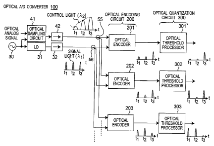
optical
encoders 201, 202 and 203 of the optical encoding circuit 200, respectively.
[0076] The respective optical encoders 20 i, 202 and 203 have period
characteristics of the power level of output signal light with respect to the
power level of inputted control light different from each other. Preferably,
there is a relationship of power-of-two among their periods (for example, the
optical encoder 201 has a period of "2T", the optical encoder 202 has a
period of "T", and the optical encoder 203 has a period of "T/2", and this
will
be described later with reference to Fig. 5). The optical encoders 201, 202
and 203 encode the input signal light according to the control light, and
output encoded signal light to the optical threshold processors 301, 302 and
303, respectively. Further, the respective optical threshold processors 301,
302 and 303 quantize inputted signal light into predetermined binary light
digital signals, and output them (while the optical threshold processors
perform 1-bit quantization and output binary optical digital signals in the
present preferred embodiment, they may output multilevel optical signals),
respectively.
(0077] Fig. 3 is a block diagram showing a detailed configuration of the
optical encoder 201 of Fig. 2. Each of the other optical encoders 202 and
203 has the same configuration as that of the optical encoder 201. Referring
to Fig. 3, the optical encoder 201 is constructed by including a nonlinear
optical loop miller 10, two photo-couplers 11 and 12, an optical isolator 13,
an optical band-pass filter 14, and an optical fiber cable 19.
CA 02546197 2006-05-16
33
[0078] In this case, in order to overcome the problem of walk-off caused
by different group delays between the control light and the signal light, the
nonlinear optical loop miller 10 is constituted by plural (at least two)
dispersion high-nonlinear optical fiber cables which are connected in
S cascade to each another, which have group delay characteristics (or
dispersion values) different from each other, and each of which has a
predetermined length (See the non-patent documents 3 and 4, for example).
The portions of the nonlinear optical loop mirror 10 near its one end and
another end are placed proximally to each other so that the portions are
optically coupled to each other, so as to form the photo-coupler 11. As
shown in Fig. 3, the following terminals are defined in the photo-coupler 11:
( 1) a terminal on the nonlinear optical loop mirror 10 at its one end
side for inputting signal light is defined as T11;
(2) a terminal at another end side for outputting optically-encoded
signal light is defined as T 12;
(3) a terminal near the one end inside the loop is defined as T21; and
(4) a terminal near another end inside the loop is defined as T22.
[0079] In addition, a further optical fiber cable 19 is arranged
proximally to an optical fiber in the nonlinear optical loop mirror 10 near
the
terminal T21 of the photo-coupler 11 so that these optical fiber cables are
optically coupled to each other, so as to form a photo-coupler 12 around
their portions which are arranged proximally to each other. As shown in Fig.
3, the following terminals are defined in the photo-coupler 12:
( 1 ) a terminal on the optical fiber cable 19 near its one end for
inputting control light is defined as T31;
(2) a terminal on the nonlinear optical loop mirror 10 near the
terminal T2 of the photo-coupler 11 is defined as T32;
(3) a terminal on the optical fiber cable 19 near another end is defined
as T41; and
(4) a terminal on the nonlinear optical loop mirror 10 closer to another
CA 02546197 2006-05-16
34
end of the nonlinear optical loop mirror IO (closer to the terminal T22) than
the terminal T2 of the photo-coupler 11 is defined as T42.
[0080] Further, another end of the optical fiber cable 19 is terminated
in a non-reflection manner via an optical isolator 13. Accordingly, the
control light enters into the optical fiber cable 19 through the one end of
the
optical fiber cable 19, and passes through the photo-coupler 12. Then, one
branched control light branched by the photo-coupler 12 is terminated in a
non-reflection state via the optical isolator 13, and another branched control
light is outputted to the loop in the nonlinear optical loop mirror 10 via the
terminal T42 of the photo-coupler 12. In addition, the optical band-pass
filter 14 for passing therethrough only component of a wavelength of W
included in the signal light is connected to another end at the terminal T 12
side of the nonlinear optical loop mirror 10.
[0081] In the case where the branching ratio of the photo-coupler 11
(for example, the branching ratio for branching an optical signal inputted
from the terminal 11 into the terminal T21 and the terminal T22) is set to
1:1 in the nonlinear optical loop mirror 10 constructed as mentioned above,
the signal light incident to the terminal T 11 is totally reflected toward the
input terminal side. In the present preferred embodiment, it is necessary
that the incident signal light is transmitted to the output terminal side.
Accordingly, a phase shift is caused only in the clockwise direction in which
control-light pulses propagate in the nonlinear optical loop mirror 10, so as
to change a phase difference between the optical signals propagating in the
clockwise direction and in the counter-clockwise direction, and due to this,
reflection or transmission of the inputted signal light can be selected. This
operational characteristic is utilized fox the threshold value processing and
the switching in the optical encoders and the optical threshold processors.
[0082] In the present preferred embodiment, by using an XPM (Cross
Phase Modulation) between the signal light and the control light, the phase
difference is caused between the pulses propagating in the clockwise
CA 02546197 2006-05-16
direction and the pulses propagating in the counter-clockwise direction in
the loop of the nonlinear optical loop mirror 10, so as to change the output
level of the signal light according to the signal level of the control light.
Namely, in the propagation of an optical signal propagating in the clockwise
5 direction in the nonlinear optical loop mirror 10, in assuming that the
signal
light has an electric field of E 1 and the control light has an electric field
of El,
the electric field E ~ receives a phase change ~ uzNL as it propagates through
an optical fiber cable having a length of L, due to the nonlinearity, and the
phase change ~~RNL is expressed by the following equation.
10 [0083) [Equation 1]
~1RNL ~ YL[ ~ ~, 1 I 2.f.2 I '~' 2 I 2J ( 1).
[0084] In this case, wt is an angular frequency of the electric field E,,
and expressed by the following equation using a coefficient y indicating the
nonlinearity.
15 [0085] [Equation 2J
Y = (~1n2)/~CAe~r) (2).
[0086] In this case, "c" is a velocity of light in a vacuum, ACrr is an
effective core cross-sectional area of the fiber, and n2 is a nonlinear
refractive
index coefficient. In addition, it is assumed that the planes of polarization
of
20 E ~ and Ez are identical to each other. Further, in the propagation in the
counter-clockwise direction in the nonlinear optical loop mirror 10, in
assuming that the signal light has the electric field of E ~, the signal light
receives a phase change ~1LNL as it propagates through the optical fiber cable
having the length of "L", and the phase change ~1L"L is expressed by the
25 following equation.
[0087] [Equation 3J
~iLNL = YL ~ E~ ~ z (3).
[0088] In this case, a phase difference ~pNL caused between the signal
lights propagating in the clockwise direction and the counter-clockwise
30 direction is expressed by the following equation.
CA 02546197 2006-05-16
36
[0089] [Equation 4]
~~1RNL = 2Y ~ E2 ( 2L (4
[0090) Due to the phase difference, the signal lights propagating in the
clockwise direction and the counter-clockwise direction interfere with each
other. Since the phase difference is proportional to the intensity of the
pulse
train of the control light, the output signal light from the nonlinear optical
loop mirror 10 of the pulse train of the signal light exhibits a periodic
characteristic with respect to the input power of the control light, as shown
in Fig. 4.
[0091] Further, in order to utilize a multi-period characteristic, it is
necessary that the control light has larger power. In order to attain this,
the
nonlinear optical loop mirror 10 can be formed by, for example, an optical
fiber cable having a higher nonlinearity. In addition, it can be considered
that the nonlinear optical loop mirror 10 preferably has a possible largest
loop length, since the intensity of the control light can be decreased with
increasing the loop length of the nonlinear optical loop mirror 10, but it is
necessary to reduce the group-delay difference as much as possible.
[0092) Fig. 5 is graphs and a block diagram showing an exemplary
operation of the optical encoding circuit 200 of Fig. 3. In Fig. 5, the
respective optical encoders 201, 202 and 203 have period characteristics of
the power level of output signal light with respect to the power level of
input
control light different from each other, respectively. In particular, there is
shown such a case where there is the relationship of power-of-two among
their periods, the optical encoder 201 has a period of "2T", the optical
encoder 202 has a period of "T", and the optical encoder 203 has a period of
"T/2". In the exemplary operation of Fig. 5, the signal light inputted at a
timing tl is encoded by the optical encoders 201, 202 and 203, then
quantized by the optical threshold processors 301, 302 and 303 (this will be
described in detail later), and is outputted as an optical digital signal
indicative of a 3-bit codes of "001". Further, in order to obtain an optical
CA 02546197 2006-05-16
37
digital signal indicative of N-bit codes, it is necessary to provide "N"
optical
encoders each having an input-to-output characteristic with a period of
T/2~N-2~ with respect to the light intensity. In this case, "N" is a natural
number indicating a quantifying bit number.
[0093] Fig. 5 is a block diagram and graphs showing a detailed
configuration and an operation of the optical threshold processor 301 of Fig.
2. Each of the optical threshold processors 302 and 303 has the same
configuration as that of the optical threshold processor 301. Referring to
Fig.
6, the optical threshold processor 301 is constructed by including a
nonlinear optical loop mirror 20, two photo-couplers 21 and 22, an optical
isolator 23, an optical band-pass filter 24, a laser diode 25, an optical
isolator 26, and an optical fiber cable 29. In this case, the nonlinear
optical
loop mirror 20, the two photo-couplers 21 and 22, the optical isolator 23, the
optical band-pass filter 24, and the optical fiber cable 29 are constructed to
be connected to each other in a manner similar to that of the optical encoder
201.
[0094] The laser diode 25 intermittently generates a train of pulses of
carrier wave light having a predetermined wavelength ~.a and a constant
signal level at the period of the sampled signals inputted from the optical
sampled signal generator 30 (the laser diode 25 may generate continuous
light instead of the train of pulses of the carrier wave light/, and outputs a
train of pulses so that train of pulses enters one end of the nonlinear
optical
loop mirror 20 (an input end of the photo-coupler 21 ) via the optical
isolator
26. On the other hand, the signal light from the optical encoder 201 enters
into the optical fiber cable 29 through one end of the optical fiber cable 29,
and passes through the photo-coupler 22 so as to be branched into two
signal lights. One signal light passing through the photo-coupler 22 is
terminated in a non-reflection state via the optical isolator 23, and another
branched signal light branched by the photo-coupler 22 is outputted to the
loop of the nonlinear optical loop mirror 20 via the photo-coupler 22. In
CA 02546197 2006-05-16
38
addition, the optical band-pass filter 24 for passing therethrough only
component of a wavelength of ~.s included in the carrier wave light is
connected to another end of the nonlinear optical loop mirror 20.
[0095) The operation of the optical threshold processor 301 constructed
as mentioned above will be described with reference to Fig. 7. Fig. 7 shows
an exemplary 1-bit quantization operation. For example, when the input-to-
output of the optical threshold processor 301 has a linear characteristic 401,
the incident signal light is outputted as it is without any quantization.
However, when the optical threshold processor 301 has, for example, a first
input-to-output characteristic 402 (with respect to the light intensity), a
smaller optical signal is converted to be smaller and closer to 0, and a
larger
optical signal is converted so as to be larger and closer to 1. Further, when
a
second input-to-output characteristic 403 (with respect to the light
intensity)
is used, it is possible to generate output light closer to one of binary
values.
Further, in order to obtain the second input-to-output characteristic 403, it
is preferable that optical threshold processors are connected in cascade to
each other in plural stages, as described in detail later.
(0096] Fig. 8 is a block diagram showing detailed configurations of the
optical encoding circuit 200 and the optical quantization circuit 300 of Fig.
2.
Figs. 9 to 11 are graphs showing exemplary operations of the respective
optical encoders 201, 202 and 203. Fig. 9 shows the exemplary operation of
the optical encoder 201, Fig. 10 shows the exemplary operation of the optical
encoder 202, and Fig. 11 shows the exemplary operation of the optical
encoder 203. In addition, Figs. 12 to 14 are graphs showing exemplary
operations of the respective optical threshold processors 301, 302 and 303.
Fig. 12 shows the exemplary operation of the optical threshold processor 301,
Fig. 13 shows the exemplary operation of the optical threshold processor 302,
and Fig. 14 shows the exemplary operation of the optical threshold processor
303.
[0097] Figs 9, 10 and 11 show the input-to-output characteristics of
CA 02546197 2006-05-16
39
the optical encoders 201, 202 and 203 with respect to the light intensity,
respectively, when the optical encoding circuit 200 and the optical
quantization circuit 300 are constructed as shown in Fig. 8. In this case, as
apparent from Figs. 9 to 11, the optical encoders 201, 202 and 203 have
period characteristics of the power level of output signal light with respect
to
the power level of input control light that are different from each other. In
particular, there is the relationship of power-of-two among their periods, the
optical encoder 241 has a period of "2T", the optical encoder 202 has a
period of "T", and the optical encoder 203 has a period of "T/2". When the
signal light shown in Figs. 9 to 11 enter into the optical threshold
processors
301, 302 and 303, respectively, the signal light can be quantized to some
degree as shown in Figs. 12 to 14, but there is still a demand for providing a
further sharp quantization characteristic.
[0098] In order to realize this, as shown in Fig. 15, optical threshold
processors are connected in cascade in plural stages, in an optical
quantization circuit 300A. Referring to Fig. 15, optical threshold processors
301 and 311 which are connected in cascade to each other in two stages are
connected subsequently to the optical encoder 201. In addition, optical
threshold processors 302, 312 and 322 which are connected in cascade to
each other in three stages are connected subsequently to the optical encoder
202. Further, optical threshold processors 303, 313, 323 and 333 which are
connected in cascade to each other in four stages are connected
subsequently to the optical encoder 203. Figs. 16 to 18 show an exemplary
operation of the optical quantization circuit 300A constructed as mentioned
above. As apparent from Figs. 16 to 18, the larger the number of stages of
optical threshold processors connected in cascade become, the sharper and
closer to rectangular the input-to-output characteristic with respect to the
light intensity can become.
[0099] Tn the above mentioned preferred embodiment, the optical
threshold processors 301, 302 and 303 are constructed using nonlinear
CA 02546197 2006-05-16
optical loop mirrors, however, the present invention is not limited to this,
and they may be constructed using nonlinear amplifying loop mirrors each
including an amplifier in the loop of the nonlinear optical loop mirror
(referred to as NALMs hereinafter, and see the non-patent document 4, for
5 example).
[0100] In the above mentioned preferred embodiment, the optical
encoders 201, 202 and 203 are constructed using nonlinear optical loop
mirrors 10, and the optical threshold processors 301, 302 and 303 are
constructed using nonlinear optical loop mirrors 20, however, the present
10 invention is not limited to this, and the optical encoders 201, 202 and 203
and the optical threshold processors 301, 302 and 303 may be constructed
using optical fiber cables or optical waveguides each having a nonlinear
optical effect such as the optical Kerr effect. In this case, the optical Kerr
effect is a phenomenon of a nonlinear optical effect generated in an optical
15 fiber cable. Generally speaking, the optical Kerr effect refers to a
nonlinear
refractive-index phenomenon, in which the refractive-index changes
depending on the intensity of the optical signal. For example, the non-
patent documents 5 and 6 disclose that such a nonlinear optical effect
realizes a period characteristic similar to that of the nonlinear optical loop
20 mirror 10.
[0101] Fig. 35 is a block diagram showing a configuration of an optical
encoder using a waveguide-type Mach-Zehnder interferometer according to a
first modified preferred embodiment of the present invention. As shown in
Fig. 35, in the optical encoder using the waveguide-type Mach-Zehnder
25 interferometer according to the first modified preferred embodiment, three
optical waveguides 81, 82 and 83 are formed, and two optical waveguides 81
and 82 out of them are placed proximally to each other at least at two
predetermined portions, so that they are optically coupled to each other at
the two predetermined portions so as to form photo-couplers 91 and 92.
30 [0102] An input terminal of the photo-coupler 91 on the optical
CA 02546197 2006-05-16
41
waveguide 82 is defined as T101, and an output terminal thereof is defined
as T 103. On the other hand, an input terminal of the photo-coupler 91 on
the optical waveguide 81 is defined as T 102, and an output terminal thereof
is defined as T104. In addition, an input terminal of the photo-coupler 92
on the optical waveguide 82 is defined as T111, and an output terminal
thereof is defined as T114. On the other hand, an input terminal of the
photo-coupler 92 on the optical waveguide 81 is defined as T112, and an
output terminal thereof is defined as T113. Further, an optical band-pass
filter 95 for passing therethrough only output signal light, which is
described
later, is connected to the output terminal T 114 of the photo-coupler 92.
[0103] In addition, between the output terminal T 104 of the photo-
coupler 91 and the input terminal T112 of the photo-coupler 92, the optical
waveguide 83 is formed proximally to the optical waveguide 81 so that they
are optically coupled to each other, to form a photo-coupler 93 at the portion
where the optical waveguides 81 and 83 are proximally to each other. An
input terminal of the photo-coupler 93 on the optical waveguide 81 is
defined as T121, and an output terminal thereof is defined as T123. On the
other hand, an input terminal of the photo-coupler 93 on the optical
waveguide 83 is defined as T122 and an output terminal thereof is defined
as T 124. Further, the output terminal T 124 of the photo-coupler 93 is
terminated in a non-reflection state via an optical isolator 94.
[0104] In the optical encoder using the waveguide-type Mach-Zehnder
interferometer constructed as mentioned above, by inputting a train of
pulses of signal light having a wavelength of ~,1 and a predetermined period
to the input terminal T 101 of the photo-coupler 91, the pulse train of signal
light is branched so as to enter into the optical waveguides 82 and 81. On
the other hand, by inputting a train of analog pulses resulted from sampling
of control light having a wavelength of ~,z and a predetermined period to the
input terminal T122 of the photo-coupler 93, the pulse train of control light
enters into the optical waveguide 81. In this case, by using the XPM
CA 02546197 2006-05-16
42
between the signal light and the control light, a phase change is caused only
in the branched signal light branched by the photo-coupler 91 on the optical
waveguide 81 in accordance with the pulse train of the control light, and
thereafter, the two branched signal lights branched by the photo-coupler 91
are re-combined to each other by the photo-coupler 92. Due to this, the
output level of the signal light can be changed according to the signal level
of
the control light. The output signal light outputted from the waveguide-type
Mach-Zehnder interferometer is extracted from the photo-coupler 92 via the
optical band-pass filter 95. The output signal light exhibits a periodic
characteristic similar to that of the nonlinear loop mirror shown in Fig. 4,
with respect to the output power of the control light. The optical encoder
using the waveguide-type Mach-Zehnder interferometer optically encodes the
control light and outputs an optically-encoded output signal light, in a
manner similar to that of the optical encoder 201 of Fig. 3. In addition, the
optical encoder in Fig. 35 may be operated as an optical threshold processor,
in a manner similar to that of the optical threshold processor 301 of Fig. 6.
[0105] Fig. 36 is a block diagram showing a configuration of an optical
encoder using a dispersion unbalanced-nonlinear optical loop mirror
according to a second modified preferred embodiment of the present
invention. The dispersion unbalanced-nonlinear optical loop mirror (referred
to as a DI-NOLM hereinafter, and see the non-patent documents 7, 8 and 9,
for example) in the optical encoder according to the second modified
preferred embodiment has been known as a nonlinear optical loop mirror
constructed only by optically-passive devices.
[0106] In the optical threshold processor using the DI-NOLM according
to the second modified preferred embodiment, an optical fiber cable 101
having a dispersion value of D1 and a length of L1 and an optical fiber cable
102 having a dispersion value of Dz (Dz<D~) and a length of La are connected
in cascade to each other, and an input end of the optical fiber cable 101 and
an output end of the optical fiber cable 102 are placed proximally to each
CA 02546197 2006-05-16
43
other so that they are optically coupled to each other, to form a photo-
coupler 105 having four terminals T 121, T 122, T 123 and T 124. In addition,
a polarization controller 106 is provided on the optical fiber cable 102 near
the terminal T124 of the photo-coupler 105, and an optical band-pass filter
104 for extracting output control light is connected to the output terminal
T122 of the photo-coupler 105 via the optical fiber cable 102 and a
dispersion-compensating optical fiber cable 103.
[0107] The optical threshold processor using the DI-NOLM having the
above mentioned configuration exhibits characteristics which depend on the
intensity of control light which is incident light, in a manner similar to
that
of the nonlinear optical loop mirror (NOLM) or the nonlinear amplifying loop
mirror (NALM). In addition, the polarization controller 106 is provided to
adjust a polarized-wave at a looped portion, the dispersion-compensating
optical fiber cable 103 compensates for the dispersions caused by the optical
fiber cables 101 and 102 in the looped portion, and the polarization
controller 106 and the dispersion-compensating optical fiber cable 103 are
essential to the DI-NOLM.
[0108] When a single optical pulse is inputted to the input terminal
T121 of the photo-coupler 105 of the DI-NOLM, the optical pulse is branched
into a pulse propagating in the clockwise direction and an optical pulse
propagating in the counter-clockwise direction with a ratio of 1:1 by the
photo-coupler 105. As to the propagation of the optical pulse propagating in
the clockwise direction, when the optical pulse enters into the optical fiber
cable 101, the pulse width thereof is increased, and the peak power thereof
is decreased, due to the larger dispersion (dispersion value Dr). Then, the
optical pulse propagates through the optical fiber cable 102 having a
significantly smaller dispersion value (Dz=0) while maintaining a decreased
peak power. On the other hand, first of all, as to the propagation in the
counter-clockwise direction, an incident pulse propagates through the
optical fiber cable 102 having the smaller dispersion value while maintaining
CA 02546197 2006-05-16
44
a larger peak power. Then, the optical pulse is entered into the optical fiber
cable 101. Since the optical fiber cable 101 has the larger dispersion value,
the optical pulse is subjected to a dispersion effect immediately after
entering into the optical fiber cable 101, and due to this, the pulse width of
the optical pulse increases, and the peak power of the optical pulse
decreases. Comparing the optical pulse propagating in the clockwise
direction with the optical pulse propagating in the counter-clockwise
direction, since the optical pulse propagating in the counter-clockwise
direction propagates over a longer distance with a higher peak power, the
optical pulse propagating in the counter-clockwise direction is influenced by
an SPM (Self Phase Modulation) in the looped portion more significantly than
the optical pulse propagating in the clockwise direction. Accordingly, due to
the difference between the SPM that the optical pulse propagating in the
clockwise direction receives in the looped portion and the SPM that the
optical pulse propagating in the counter-clockwise direction receives in the
looped portion, it is possible to transmit or reflect the optical pulse of
incident control light. The DI-NOLM has advantages that it requires no
signal light and no optical amplifier, it is constituted only by optically-
passive devices, it can totally reflect continuous waves (CW) by using the
3dB photo-coupler 105, and the length of the optical fiber cable forming the
looped portion can be set to be relatively longer because it employs the
dispersion-compensating optical fiber cable 103. By the use of the DI-NOLM,
it is possible to easily perform optical threshold processing with only
optically-passive devices.
[0109] The optical threshold processor using the DI-NOLM constructed
as mentioned above can be operated in a manner similar to that of the
optical threshold processor 301 of Fig. 6.
[0110] Fig. 37 is a block diagram showing a configuration of an optical
encoder using a Kerr shutter having the optical Kerr effect according to a
third modified preferred embodiment of the present invention. As shown in
CA 02546197 2006-05-16
Fig. 37, the Kerr shutter having the optical Kerr effect is constructed by
including a high-birefringence optical fiber cable 1 I 1 having a
birefringence
of, for example, 2.0 or more and a polarizes I 12 connected thereto. The Kerr
shutter having the optical Kerr effect is the same as that disclosed in, for
5 example, Fig. 6.1 of the non-patent document 5.
[O111J Referring to Fig. 37, signal light and control light are both
inputted to the high-birefringence optical fiber cable 111 through its input
end, so that they are angled by 45 degree with respect to each other with a
linear polarization. When there is no signal light, the control light is
10 interrupted by the polarizes 112, and is not outputted from the output end.
However, when the signal light is inputted, the polarization of the control
light is rotated due to the birefringence caused by the signal light, which
allows the control light to pass through the polarizes 112 and to be
outputted from the polarizes 112. The output power of the control light
15 periodically changes depending on the intensity of the signal light.
[0112] The optical encoder using the Kerr shutter having the optical
Kerr effect which is constructed as described above optically encodes the
control light, and outputs optically-encoded output signal light, in a manner
similar to that of the optical encoder 201 of Fig. 3. In addition, the optical
20 encoder of Fig. 37 can be operated as an optical threshold processor, in a
manner similar to that of the optical threshold processor 301 of Fig. 6.
FIRST IMPLEMENTAL EXAMPLE
[0113] Fig. 19 is a block diagram showing a detailed configuration of an
experimental system according to the present preferred embodiment. In the
25 experimental system of Fig. 19, a fiber ring laser (FRL) 50 generates an
optical analog signal having a sampling frequency of, for example, 80 GHz,
and outputs the optical analog signal to an optical splitter 57. The optical
splitter 57 splits an inputted optical analog signal into two signals, and
outputs the two signals to optical band-pass filters 51 arid 52, respectively.
30 The optical band-pass filter 51 band-pass filters an inputted optical
analog
CA 02546197 2006-05-16
46
signal so as to pass therethrough only components of a predetermined
wavelength ~,~ included in the inputted optical analog signal, and outputs a
train of pulses having a pulse width of, for example, 2 picoseconds to an
optical splitter 56. The optical splitter 56 splits an inputted optical analog
signal into three signals, and outputs the three signals to nonlinear optical
loop mirrors 10 of respective optical encoders 201, 202 and 203 via delay
circuits 15 and optical isolators 16.
[0114) On the other hand, the optical band-pass filter 52 band-pass
filters an inputted optical analog signal so as to pass therethrough only
components of a predetermined wavelength ~,2 included in the inputted
optical analog signal, and outputs a train of pulses having a pulse width of,
for example, 8 picoseconds to an optical modulator 53. The optical
modulator 53 modulates an inputted optical analog signal according to a
data signal from a data signal generator 54, and outputs a modulated optical
analog signal to an optical splitter 56. In this case, the wavelength ~,z is
close to the wavelength ~,~. The optical splitter 55 splits an inputted
optical
analog signal into three signals, and outputs the three signals to the loops
of
the nonlinear optical loop mirrors 10 via photo-couplers 12 of the respective
optical encoders 201, 202 and 203.
[O1 I5] The respective optical encoders 201, 202 and 203 encode the
signal light according to the signal level of control light, and the encoded
signal light is outputted to the loops of the nonlinear optical loop mirrors
20
via optical amplifiers 2? and optical isolators 28 and via the photo-couplers
22 of the respective optical threshold processors 301, 302 and 303. On the
other hand, the carrier wave light having the wavelength of 7~s (in this case,
the wavelength ~,s is close to the wavelength W) generated by the laser diodes
25 is inputted to the loops of the nonlinear optical loop mirrors 20 of the
respective optical threshold processors 301, 302 and 303 via the optical
isolators 26. Accordingly, each of the optical threshold processors 301, 302
and 303 quantizes the carrier wave light according to the signal level of the
CA 02546197 2006-05-16
47
signal light, and a quantized carrier wave light is outputted to an external
optical circuit via the optical band-pass filter 24.
[0116] Figs. 20 to 22 are graphs showing exemplary operations of the
encoding processing in the optical encoding circuit 200 of Fig. 19. Fig. 20
shows the exemplary operation of the encoding processing in the optical
encoder 201, Fig. 21 shows the exemplary operation of the encoding
processing in the optical encoder 202, and Fig. 22 shows the exemplary
operation of the encoding processing in the optical encoder 203. In addition,
Fig. 23 is a graph showing the 3-bit encoded value (# 1, #2 and #3) with
respect to the amplitude of input analog pulses of the control light (~,a)
which
is resulted from the encoding processing using the optical encoding circuit
200 of Fig. 19. As shown in Figs. 20 to 22, it is possible to perform proper
encoding according to the input power level of the inputted control light, by
setting the input-to-output characteristics of the respective optical encoders
201, 202 and 203 with respect to the light intensity. In addition, as shown
in Fig. 23, the encoding is performed so that an encoded value corresponds
to the amplitude of input analog pulses of the control light (~.z) in an one-
to-
one manner, and, as previously described, the input-to-output
characteristics of the respective optical encoders 201, 202 and 203 with
respect to the light intensity (particularly, the period characteristics of
the
nonlinear optical loop mirrors 10) can be changed so as to provide a degree
of freedom to the encoding processing.
[0117] Fig. 24 is a diagram showing the 3-bit encoded values (#1, #2
and #3) and the pulse waveforms thereof which are resulted from encoding,
when the amplitude of analog pulses after processing by a single optical
threshold processor is changed, in the case where the experimental system
is constructed by using ideal nonlinear optical loop mirrors in Fig. 19. As
apparent from Fig. 24, it is possible to obtain optical digital signals which
are properly encoded according to the amplitude of analog pulses.
SECOND IMPLEMENTAL EXAMPLE
CA 02546197 2006-05-16
48
[0118] Next, there will be described simulations conducted by the
present inventors and the results thereof, hereinafter. The specification of
the simulations is shown in the following tables.
[0119]
[Table 1 )
Specification of Simulations
Type of the optical fiber High-nonlinear optical fiber
cable cable
Loss 0.25 dB/km
Zero-dispersion wavelength 1550 nm
Dispersion slope 0.016 ps/ nmz/ km
Nonlinearity 12.6 W-lkm2
Length 500 m
(Remarks) A link simulator manufactured by R-soft Corporation was used.
[0120]
(Table 21
Fiber ring laser (FRLJ
61
Repetition frequency 10 GHz
Center wavelength 1560 nm
Pulse width 10 ps
Peak power 20 mW
Average power 3.24 dBm
CA 02546197 2006-05-16
49
[0121]
[Table 31
Fiber ring laser (FRL)
62
Repetition frequency 10 GHz
Center wavelength 1550 nm
Pulse width 40 ps
Peak power 0 to 2 W
Average power
to 29 dBm
[0122] Fig. 25 is a black diagram showing a configuration of an
experimental system for a first simulation according to the present preferred
embodiment. Referring to Fig. 25, a fiber ring laser (FRL) 61 generates signal
light having a wavelength of W, and outputs a generated signal light to the
loop of the nonlinear optical loop mirror 10 the optical encoder 201. On the
other hand, a fiber ring laser (FRL) 62 generates control light having a
wavelength of ~,2, and outputs a generated control light to the loop of the
nonlinear optical loop mirror 10 of the optical encoder 201 via an optical
delay circuit 63 and the photo-coupler 12. The optical encoder 201 encodes
the signal light according to the signal level of the control light, and
outputs
encoded signal light via the optical band-pass filter 14.
[0123] Fig. 26 is a graph showing peak power of pulses of the signal
light (~,1) with respect to peak power of pulses of the control light (~,z),
showing results of the first simulation. As apparent from Fig. 26, as results
of the first simulation of Fig. 25, simulated values close to theoretical
values
of the period characteristic are obtained. In this simulation, four-optical-
wave mixing was neglected. Further, it can be considered that the
differences between the simulated values and the theoretical values are due
to the walk-off caused by the dispersion in the nonlinear optical loop mirror
10.
THIRD IMPLEMENTAL EXAMPLE
CA 02546197 2006-05-16
[0124] Fig. 27 is a block diagram showing a configuration of an
experimental system for a second simulation according to the present
preferred embodiment. In the second simulation of Fig. 27, as compared
with the simulation of Fig. 25, levels of output signal light were measured,
5 when control light with a peak power of 1 W generated by the fiber ring
laser
62 was attenuated by three stages of 3 dB photo-couplers 71, 72 and 73 so
as to generate control light having three optical signal levels, and generated
control light are inputted to the optical encoders 201, 202 and 203,
respectively. Assuming that the level of the control light from the photo-
10 coupler 7I is 1, the level of the control light from the photo-coupler 72
is 1/2,
and the level of the control light from the photo-coupler 73 is 1 / 4.
[0125] Figs. 28 to 30 show results of the second simulation of Fig. 27.
Fig. 28 is a waveform diagram showing a pulse waveform of the signal power
from the optical encoder 201, Fig. 29 is a waveform diagram showing a pulse
15 waveform of the signal power from the optical encoder 202, and Fig. 30 is a
waveform diagram showing a pulse waveform of the signal power from the
optical encoder 203. As apparent from Figs. 28 to 30, the second simulation
results in signal light encoded according to the levels of the control light
inputted to the respective optical encoders 201, 202 and 203.
20 FOURTH IMPLEMENTAL EXAMPLE
[0126] Fig. 31 is a block diagram showing a configuration of an
experimental system for a third simulation according to the present
preferred embodiment. In the third simulation of Fig. 31, as compared with
the simulation of Fig. 27, the peak power of the control light generated by a
25 fiber ring laser 62 is changed to 1.5 W, and the other configurations are
the
same as those of the second simulation.
[0127] Figs. 32 to 34 show the results of the third simulation of Fig. 31.
Fig. 32 is a waveform diagram showing the pulse waveform of the signal
power from the optical encoder 201, Fig. 33 is a waveform diagram showing
30 the pulse waveform of the signal power from the optical encoder 202, and
Fig.
CA 02546197 2006-05-16
51
34 is a waveform diagram showing the pulse waveform of the signal power
from the optical encoder 203. As apparent from Figs. 32 to 34, the third
simulation of Fig. 31 results in signal light encoded according to the levels
of
the control light inputted to the respective optical encoders 201, 202 and
203. In addition, comparing the results of the simulations of Figs. 28 to 30
and Figs. 32 to 34, it can be seen that encoding was properly attained.
[0128] As described above, according to the optical A/D converter 100
according to the present preferred embodiment, sampled optical analog
signals can be optically A/ D-converted into optical digital signals, the
upper
limit of the sampling frequency can be the order of several hundreds GHz to
several THz, in principle. Assuming that the limit of the sampling frequency
of the A/D conversion for the electric circuit is several tens of GHz, it is
possible to realize speeding-up by about two orders of magnitude. In
addition, since the inputting and outputting are performed with optical
signals, the optical A/ D converter 100 is suitably applied to optical
networks.
SECOND PREFERRED EMBODIMENT
(0129] There will be described a nonlinear optical loop mirror (referred
to as a NOLM hereinafter) for use in the above mentioned optical A/D
converter 100 and the like, hereinafter.
[0130] A conventionally-used NOLM has a relationship between the
input light power and the output light power, as shown in Fig. 39. In this
case, the terms of "the input light power" refer to the input power of signal
light in case of an interference switch (self switch) which utilizes a phase
shift caused by SPM (self-phase modulation) of an optical pulse, and the
terms refer to the input power of control light in case of an interference
switch (XPM switch) which utilizes a phase shift caused by XPM (cross-phase
modulation) between the control light and the signal light. In addition, the
terms of "the output light power" refers to the output optical power of signal
light outputted from a transmission port of the NOLM. In addition, the
control light and the signal light are in a form of pulses hereinafter, except
CA 02546197 2006-05-16
52
when they are particularly specified.
[0131] When the input power is sufficiently small, the output power is
also suppressed. On the ether hand, when the input power is increased, the
output power is also increased along a sinusoidal wave curve, and the
S output power reaches a peak value when the input power is P~. By utilizing
this transfer function, it is possible to realize a switch capable of
controlling
the, reflection and transmission of signal light depending on presence and
absence of the control light. Also, when a signal having amplitude fluctuated
by transfer thereof is used as the control light, and switching of probe light
is
caused therefrom, even if the 0 level and the 1 level are fluctuated by noise,
the fluctuation of the output is suppressed, which is expected to have a
waveform reshaping effect. As described above, the NOLM having a transfer
characteristic of a half-period sinusoidal-wave curve have been realized and
utilized.
[0132] Such a NOLM was originated with our suggestion of an
interference switch which utilizes a phase shift caused by SPM of optical
pulses (See the non-patent document 3, for example) and an interference
switch which utilizes a phase shift caused by XPM between control light and
signal light (See the non-patent document 10, for example) . In relation to
them, there are a NOLM using a high-nonlinear fiber (See the patent
document 2, for example), signal processing which utilizes FWM in a NOLM
(See the patent document 3, for example), a NOLM capable of suppressing
walk-off of control light and signal light for increasing the efficiency of
XPM
(See the patent document 5, the patent document 2, the patent document 6,
the patent document 7, the patent document 8 and the patent document 10,
fox example) and a configuration in which fibers have a dispersion
management configuration having an average dispersion of zero to reduce
walk-off and also FWM which would cause reduction of the power of control
light is suppressed to increase the efficiency of XPM (See the patent
document 10, for example). Tn addition, various characteristics of NOLMs
CA 02546197 2006-05-16
53
about polarization have been known (See the patent document 4 and the
patent document 9, for example).
[0133] On the other hand, in an optical encoder and an optical
threshold processor, a NOLM having a sinusoidal-wave curve transfer
function with plural periods as shown in Fig. 40 is utilized, however, such a
NOLM has not been realized in the prior art. As will be described later, a
NOLM according to the preferred embodiment of the present invention has a
transfer function with one or more periods and can exhibit characteristics
suitable for various types of optical signal processing including optical A/ D
conversion.
[0134] Fig. 38 shows a configuration of a NOLM 500. The NOLM 500 is
constituted by an optical fiber 501, a photo-coupler 502 connected thereto
so as to branch an optical signal 530 inputted from an optical-signal input
end 510 into two optical signals and output the two optical signals to both
ends 511 and 512 of the optical fiber 501, respectively, and so as to branch
and output optical signals outputted from the both ends 511 and S 12 of the
optical fiber 501 to the above mentioned optical-signal input end 510 and a
further output end 513, a control-light inputting means 524 for inputting
control light 531 to the above mentioned optical fiber 501, and a high
nonlinear optical fiber (referred to as an HNLF hereinafter) 504 which is a
nonlinear medium placed on the optical path of the above mentioned optical
fiber 501. Tn this case, the input signal light 530 has an input power of Pin
and a wavelength of ~,s, and the control light 531 has a peak power of PC, an
average power of Pave and a wavelength of ~,c.
[0135] The signal light S30 with the input power of Pin which is
inputted from the optical-signal input end S 10 is branched into propagating
light 532 which receives no phase change and propagating light 533 having
a phase proceeding by ~c/2 through the photo-coupler 502, and these
propagating lights 532 and 533 propagate in the clockwise and counter-
clockwise directions on the figure, respectively, in the loop formed by the
CA 02546197 2006-05-16
54
optical fiber 501. The propagating light 532 is coupled to the control light
531 having the peak power of Pc and an average power of Pave which is
inputted from the control-light inputting means 524, so that they are
superimposed on each other over a possible largest range. Then, the
propagating light 532 passes through the HNLF 504, which is a nonlinear
medium having a nonlinearity coefficient of y and a length of "L", and is
inputted to the photo-coupler 502 through the optical fiber end 512.
[0136] In addition, the propagating light 533 propagates in the loop
formed by the fiber 501 in the counter-clockwise direction in the figure.
Then, the propagating light 533 passes through the HNLF 504, and is
inputted to the photo-coupler 502 through the optical fiber end 511 almost
without being superimposed on the control light.
[0137) When there is no control light, there is hardly a difference
between the phase shift which is generated in the light propagating in the
clockwise direction and the phase shift which is generated in the light
propagating in the counter-clockwise direction. Consequently, at the output
end 513, the component of the propagating light 532 propagating in the
clockwise direction which has received no phase shift and the component of
the propagating light 533 propagating in the counter-clockwise direction
which has received a phase shift of n/2 at the photo-coupler 502 twice are
cancelled by each other, and this leads to an output of 0. In addition, at the
input end 510, the respective components of the propagating lights 532 and
533, which have both received a phase shift of ~/2 at the photo-coupler 502
a single time, are reinforced by each other, and therefore, returned light
having substantially the same power as the input power is outputted to the
input end 510 in the direction opposite to that of the input signal light 530.
[0138] When the control light 531 is present, the propagating light 532
propagates through the HNLF 504 while being superimposed on the control
light 531, and this generates a phase shift in the propagating light 532 due
to cross-phase modulation (XPM) depending on the power of the control light
CA 02546197 2006-05-16
531 which is caused between the propagating light 532 and the control light
531. On the other hand, the propagating light 533 hardly generates a phase
shift caused by the XPM, and this causes a phase shift difference between
the propagating light 532 and the propagating light 533, depending on the
5 power of the control light 531. This enables controlling the power outputted
to the input end 510 and another output end 513.
[0139] In this system, a power ratio of the output signal light 534
having an output power of Pout to the input signal light 530 having an input
power of Pin is expressed by the following transfer function:
10 [0140] jEquation 5]
Pout/Pin = [1-cos(~xPM)]/2 (5), and
[Equation 6]
~XPM = 2y(Pc-Pave)L (6).
[0141] In this case, in order to realize a transfer function having one or
15 more periods, and more preferably, two or more periods, it is necessary
that
the phase shift difference ~XPM =2y(Pc-Pave) L in the signal light due to the
XPM generated between the control light and the signal lights is at least 2n
(corresponding to a single period and Pz in Fig. 40) or 4~c(corresponding to
two periods and P4 in Fig. 40). Namely, it is preferable that the cross-phase
20 modulation (XPM) which is caused between the two branched optical signals
and the above mentioned control signal generates a phase shift difference of
2n or more between these optical signals.
[0142] Therefore, the phase shift can be increased by efficiently
generating XPM with the following methods.
25 (i) some or all of the nonlinearity and the distance of the HNLF 504
which is a nonlinear medium and the power of the control light 531 are
increased.
(ii) the polarizations of the control light 531 and the signal light 530
are optimized (the efficiency of occurrence of XPM is maximized) .
30 (iii) in order to prevent the wavelength difference between the control
CA 02546197 2006-05-16
56
light 531 and the signal light 530 from generating a group delay (referred to
as walk-off hereinafter) due to dispersion, the dispersion value of the HNLF
504 or the arrangement of the wavelengths of the signal light 530 and the
control light 531 with respect to the given dispersion value is changed to
suppress the walk-off.
(iv) the positions of the control light 531 and the signal light 530 in
the time axis are optimized with considering the walk-off.
[0143) In addition, in order to realize the above mentioned (iii), it is
possible to employ a method of using a fiber having an arbitrary length and a
dispersion value of zero (a dispersion flat fiber; DFF) or a method of using a
conventional dispersion shift fiber (DSF) having a constant dispersion slope
in the fiber 504 and setting the zero-dispersion wavelength ~,o of the fiber
(DSF) between the wavelength ~,c of the control light 531 and the wavelength
~.s of the signal light 530. In the case of the latter method, when the zero-
dispersion wavelength of the fiber (DSF) is fluctuated in the longitudinal
direction, this will cause the walk-off proportional to the product of the
wavelength difference ~~, between the wavelength ?~c and the wavelength ~,s
and the dispersion value and, therefore, it is necessary to reduce the product
to the extent that the occurrence of the walk-off is not problematic. In this
case, it is preferable that the absolute value of the product of the
wavelength
difference between the above mentioned control light signal and the above
mentioned optical signal and the dispersion value of the above mentioned
nonlinear medium is equal to or smaller than a value which suppresses the
walk-off and also causes the phase shift difference of 2~c or more between the
two branched optical signals, where the phase shift is caused by cross-phase
modulation (XPM) which occurs among these optical signals and the control
light signal.
[0144) In any of the cases, the wavelength ~,c is made closer to the zero-
dispersion wavelength ho and the dispersion value for the wavelength ~,c
becomes closer to 0. In this case, a parametric gain is caused in the signal
CA 02546197 2006-05-16
57
light 530 due to degenerate four-wave mixing (FWM) caused by the control
light 53I which serves as pump light. Due to this phenomenon, the signal
light 530 is amplified as it propagates in the clockwise direction along with
the control light 531, while the signal light 530 propagating solo in the
counter-clockwise direction receives no gain, and this leads to a state where
the powers of the propagating lights 532 and 533 are unbalanced. When
such unbalance becomes prominent, the output powers obtained at the
input powers Pz and P4 in Fig. 40 will not become sufficiently smaller, and
this will cause serious problems.
[0145] The important point of the transfer function of Fig. 40 is that the
output powers with respect to the input powers Pz and Pa are equal to or
smaller than an optimally-set threshold value, assuming that the peak value
(the output power value with respect to the input powers P1 and Ps) is 1.
[0146] Namely, by applying a previously-set threshold value to the
output signal of the NOLM, it is possible to realize binary signal processing
which is basic digital information processing. For example, in the case
where the threshold value is set to 0.5, when the above mentioned
parametric processing causes a gain larger than 3dB with respect to input
powers of P~ and P4, this causes light which is not intended to be
transmitted due to phase interference to be transmitted since its power
exceeds 0.5, which makes it impossible to perform binary signal processing.
Generally speaking, it is necessary that an inequality of G<2Tth-~ 1 holds
with respect to the threshold value Tth (0<Tth< 1; the ratio between the
output power at Pz and P4 and the output power at P1 and Pa) and the
parametric gain G (> 1; the ratio between the input power and the output
power of propagating light 532 in the nonlinear medium). This enables
suppressing the output power with respect to the input powers P~ and Pz to
be equal to or smaller than a desired threshold value, so as to realize
optical
binary signal processing including quantization and encoding processings for
optical A/D conversion. This fact has not been known, although it is a
CA 02546197 2006-05-16
58
significantly important knowledge for realizing a NOLM having a transfer
function of Fig. 40.
[0147] Therefore, in order to suppress the parametric gain that the
signal light 530 propagating in the same direction as that of the control
light
531 receives from the control light 531 to be equal to or smaller than a
predetermined value (for example, 3dB), the following method will be
suggested in the preferred embodiment of the present invention. The non-
patent document 5 describes that, when continuous light having a frequency
of we which is a linearly-polarized light is used as pump light in an optical
fiber, generally speaking, the degenerate parametric gain "G" that signal
light
having a frequency of ws and propagating in the same direction at the same
polarization state as when the pump light receives is expressed by the
following equation. The terms of "pump light" used in the discussion
corresponds to the control light in the NOLM according to the preferred
embodiment of the present invention.
[0148] [Equation 7]
G(z) = 1+(~y~POZ/g2)Slnh2(~) (~)~
[Equation 8]
g2 = 'Y2p0'~-KZ/4 (8)~
[Equation 9]
K = Ok+2yPo (9), and
[Equation 10]
Ok = ~w2ko'~ ( 10).
[0149] Tn these equations, z, ~y, Po, ko" and 0~ designate the fiber length
[m], the nonlinearity constant [W-lm-I] of the fiber, the power [W) of the
pump light, the dispersion value [sl/m] of the fiber, and the frequency
difference [s-j] between the pump light and the signal light, respectively,
and
the effects of dispersion and loss of four and larger orders in the fiber are
neglected. By giving these values, the parametric gain that the signal light
receives can be uniquely determined from the equations (7) to (10). For
CA 02546197 2006-05-16
59
example, in the case of z=0.32 [km], y=17.5 [W-~km-1] and Po=2 [W], the gain
change with respect to the value of Ow will be considered. Further, it is
assumed that a fiber dispersion value D [ps/nm] which satisfies a
relationship of ko"=-1.284D with respect to k" [psl/ kmj is employed as the
fiber dispersion value, and the frequency difference ~w can be expressed by
~w=2~cc07~ j~, using the wavelength difference ~~.= ) ~,c:-~,s ~ between the
pump
light and the signal light. Further, c=2.998*10$ [m/s] and ~,=1.55[~mj
designate the velocity of light in a vacuum and the wavelength of carrier
wave. First, Fig. 41 shows the parametric gain obtained from the
calculations of the equations (7) to ( 10), in the case where the wavelength
difference ~~. between the pump light and the signal light is set to 10 nm and
the fiber dispersion value D(~,c) for the wavelength ~,c of the pump light is
changed.
[0150] Referring to Fig. 41, a large gain observed at D-1[ps/nm/km] is
known as a modulation instability phenomenon which occurs in an
anomalous dispersion region. For example, in order to suppress the
parametric gain to be equal to or smaller than 3dB, it is necessary that the
dispersion value is set to be smaller than the dispersion value D' at a point
"A" in the normal dispersion region or larger than the dispersion value D" at
a point "B" in the anomalous dispersion region. In Fig. 41, generally
speaking, ~ D' ~ < 1 D" ~ , and it is preferable to utilize the normal
dispersion
value D' having a smaller absolute value, in view of the reduction of walk-off
Which is proportional to the absolute value of the dispersion value. In
addition, when pulses having large energy propagate through an anomalous
dispersion fiber, this will excite higher-order solitons so as to degrade the
waveform of the control light, which may result in degradation of the
efficiency of XPM. Accordingly, in view of this point, it is not preferable to
use the anomalous dispersion value D", as compared with the use of D'.
However, if the walk-off and the waveform degradation due to soliton
excitation are not problematic, it is also possible to set the fiber
dispersion
CA 02546197 2006-05-16
value to be anomalous dispersion, under the condition of D>D" in Fig. 41.
[0151] Next, Fig. 42 shows the parametric gain obtained from the
equations (7) to ( 10), in the case where the dispersion value "D" is set to -
0.62 [ps/nm/kmj and the wavelength difference 0~,= ~ ~.c-7~s ~ between the
5 pump light and the signal light is changed. Fig. 42 shows that the
pararnetric gain can be suppressed by increasing ~~. When it is desired to
minimize the influence of the dispersion such as walk-off and waveform
expansion under the condition where the parametric gain should be set to be
equal to or smaller than 3dB, the wavelength difference between the pump
10 light and the signal light can be set to a value of 0~,' at a point "C" in
Fig. 42.
[0152] There has been described that, in order to suppress the
parametric gain to be equal to or smaller than a certain value, it is
effective
to set the fiber dispersion value for the wavelength of the pump light to a
value smaller than a minimum dispersion value (corresponding to the point
15 "A" of Fig. 41) which can provide a parametric gain equal to or larger than
the certain value or larger than a maximum dispersion value (corresponding
to the point "B" of Fig. 41) which can provide a parametric gain equal to or
larger than the certain value, and it is effective to set the wavelength
difference between the pump light and the signal light to be larger than a
20 maximum wavelength difference (corresponding to the point "C" of Fig. 42)
which can provide a parametric gain equal to or larger than the certain value.
Also, the points A, B and C of Figs. 41 and 42 may be provided on envelopes
in the respective graphs. Namely, it is effective to satisfy any one of the
following conditions.
25 (a) The dispersion value of the nonlinear medium is equal to or
smaller than a minimum dispersion value which causes the paxametric gain
that occurs between the above mentioned optical signal and the above
mentioned control light signal to be equal to or larger than a predetermined
value.
30 (b) The dispersion value of the nonlinear medium is equal to or larger
CA 02546197 2006-05-16
61
than a maximum dispersion value which causes the parametric gain that
occurs between the above mentioned optical signal and the above mentioned
control light signal to be equal to or larger than a predetermined value.
Tn addition, it is preferable that the wavelength difference between the
S above mentioned control light signal and the above mentioned input optical
signal is larger than a maximum wavelength difference which causes a
parametric gain equal to or larger than a predetermined value, between the
above mentioned optical signal and the above mentioned control light signal.
[0153] Considering the parametric processing which occurs between
the control light S31 and the signal light 530 (propagating light 532] which
propagate in the same direction in the NOLM 500 of Fig. 38 being studied,
errors may be induced in the result of the calculations of the equations (7)
to
( 10), due to various factors such as the fact that the control light and the
signal light are pulses having power which change depending on time, not
continuous light having a single frequency, and the fact that the efficiency
of
the FWM between the control light and the signal light pulses is degraded
due to walk-off and disagreement of the polarization among the pulses.
However, the dependence of the parametric gain shown in Figs. 41 and 42
on various types of parameters can be experimentally determined even with
respect to pulses in the NOLM 500, which can provide concrete instructions
on how to set the dispersion value or the wavelength difference.
[0154] Figs. 43 and 44 show a fiber wavelength dispersion
characteristic and arrangement of the wavelengths of control light and signal
light which can effectively suppress the parametric gain which is caused
between control light 531 and signal light 530 (propagating light 532)
propagating in the same direction in the NOLM 500. Fig. 43 shows a fiber
wavelength dispersion characteristic in the case of dD/d~,>0, and a
relationship of ~,c>~s>~.o holds. Further, in Figs. 41 and 42, it is assumed
that the relationships of D(~,c)<D' and 0~,= [ ~,c-~.s ~ >~~.' are satisfied
with
respect to the dispersion value D' and the wavelength difference 0~,' of this
CA 02546197 2006-05-16
62
case. Fig. 44 shows a case of dD/d?~<0, and the other conditions are the
same as those of Fig. 43. In addition, in the case where the dispersion value
"D" of the above mentioned nonlinear medium differentiated with respect to
the wavelength ~, is negative (dD/d~,<0) with respect to the wavelengths of
the above mentioned input optical signal and the above mentioned control
light signal, it is possible to satisfy a relationship of a,o<~.s<~.c.
[0155] As the normal dispersion value D (~,c(<0)) for the wavelength ~.c
of the control light 531 which is pump light and the wavelength difference ~~,
between the control light 531 and the signal light 530 are increased, the
parametric gain can be decreased. However, when the normal dispersion
value D and the wavelength difference 0~, are excessively increased, this will
cause an increase of walk-off and degradation of the efficiency of XPM due to
distortion of the waveforms of respective pulses caused by dispersion, which
is not preferable. Accordingly, by designing the NOLM for optimally setting
the walk-off and the time difference between the control light 531 and the
signal light 530 or their polarizations such that the parametric gain that the
signal light 530 receives is equal to or smaller than a certain value and also
the reduction of the efficiency of XPM is prevented, it is possible to realize
a
NOLM having a transfer function of Fig. 40. Further, since the walk-off is
proportional to the absolute value of the product of the wavelength difference
~~. between the control light 531 and the signal light 530 and the dispersion
value D (~,c) for the wavelength ~,c of the control light 531, it is
preferable to
reduce the product. Also, even if the wavelengths of the control light and the
signal light are interchanged in Figs. 43 and 44, this will cause no problem
as long as a relationship of D(T,c) <D' is satisfied. Further, by structuring
the
NOLM such that the polarizations of the fibers and the nonlinear medium in
the loop or the states thereof are always maintained, it is possible to
efficiently generate XPM. Concretely speaking, the control light and the
signal light can be made substantially identical linearly-polarized light, by
using polarization maintenance fibers. In this case, the gain of the signal
CA 02546197 2006-05-16
63
light caused by the parametric processing is also increased, but the
previously-described designing method can be employed in view of this point.
[0156] A method for designing a NOLM having a transfer function of Fig.
40 has been described, and Fig. 45 shows the method briefly. The NOLM
according to the preferred embodiment of the present invention is designed
according to the procedure of designing processing shown in a flow chart of
Fig. 45.
[0157] Referring to Fig. 45, first of all, at step S1, the transfer function
of the NOLM is determined, namely, the maximum value Amax of the angle ~
in 1-cos ø~ is determined. Next, at step S2, a threshold value suitable for
desired signal processing is determined for the transfer function and, at step
S3, fiber parameters for use in the NOLM and the conditions on the control
light are provisionally determined. Then, it is determined at step S4 whether
or not the maximum phase shift value caused by XPM reaches the maximum
angle Amax. If YES at step S4, the control flow goes to step S5. On the
other hand, if NO at the determination of step S4, the control flow returns to
step S3. Further, at step S5, it is determined whether or not the parametric
gain that the signal light receives from control light is equal to or smaller
than the pre-set threshold value, under conditions of the angle ~ is 2n~ (n=1,
2, ...) in the transfer characteristic. If YES at step S5, the control flow
goes
to step S6. On the other hand, if NO at the determination of step S5, the
control flow returns to step S3. Further, at step S6, the design is settled
under the current conditions, and the designing processing ends.
[0158] With the preferred embodiment of the present invention, there is
realized a NOLM capable of providing a controllable range for the output
light power exceeding a single period and also suppressing the output light
power at phase differences of 2n~(n=1, 2, ....) to be equal to or smaller than
a
threshold value required for optical signal processing (for example,
quantization and encoding processings for optical analog-to-digital
conversion), with respect to the peak power. One of applications thereof is
CA 02546197 2006-05-16
64
optical A/D conversion. As the other possible aspects, the NOLM may be
applied to decoding for multi-level communication such as QAM, PSK, ASK.
From a different viewpoint, it is possible to realize a switching device which
actively utilizes the parametric gain that signal light receives from control
light, rather than switching which utilizes XPM in a NOLM. In this case, it is
preferable that the power value of the above mentioned output optical signal
when the phase shift difference caused between the two branched optical
signals is 2nn (where "n" is an integer equal to or larger than 1), is
processed
as "0" in optical analog-to-digital conversion processing, and the above
mentioned phase shift difference is caused by the cross-phase modulation
(XPM) between these optical signals and the control light signal.
FIFTH IMPLEMENTAL EXAMPLE
[0159) Fig. 46 shows an aspect of a NOLM 550 according to the
preferred embodiment of the present invention. On the assumption that
signal processing is performed in the case where the threshold value for the
transfer function of the NOLM 550 is set to 0.5, there will be described later
an implemental example of the NOLM adaptable thereto.
[0160) In the NOLM 550, signal light is inputted to an input end 580,
and the signal light is branched into two signal lights by a 3dB-coupler 552.
The two signal lights propagate through an optical fiber 551 in the opposite
directions, respectively. The signal light propagating in the clockwise
direction is combined with control light inputted from a control-light input
end 571 via a WDM coupler 574, so that they are superimposed on each
other over a wide range, and then the signal light propagates through an
HNLF (high nonlinear fiber) 554 via a l7dB coupler 553. The HNLF 554
used in the NOLM 550 has a fiber length of 380 m, a nonlinearity constant of
17.5 W-lkm-1, a zero-dispersion wavelength of 1575 nm, a dispersion slope of
0.027 ps/nm, and a fiber loss of 0.67 dB/km. In addition, the control light
having a train of pulses having a width of about 15 ps has a wavelength of
1552 nm, the signal light having a train of pulses having a width of about
CA 02546197 2006-05-16
3.4 ps has a wavelength of 1568 nm, each of these pulse trains has a
repetition frequency of 10 GHz, and the wavelength difference between the
control light and the signal light is 16 nm. In addition, a dispersion value
of
the HNLF 554 is -0.62 ps/nm/km, namely a normal dispersion value, for the
5 wavelength of the control light. The dispersion value of the HNLF 554 is a
normal dispersion value in the above mentioned example, however, it may be
an anomalous dispersion value.
[0161] In order to generate an XPM efficiently, the amount of the time
delay of the signal light and the polarization of the control light are set to
10 optimal states. The concrete contents of the stated is described below.
[0162] (A) Adjustment of the polarization of the signal light: First of all,
the signal light is entered into the NOLM 550 through the input end 580, at
a state where the control light does not enter the NOLM 550, and a
polarization controller (PC) 592 of the loop is operated so as to create such
a
15 state that the signal light is totally reflected back to the input end.
Then, the
signal light is detected using an optical circulator 598 at a reflected-light
photo-detection end 593. Concretely speaking, the polarization controller
(PC) 592 in the loop is adjusted so that the signal lights propagating in the
clockwise direction and the counter-clockwise direction which are resulted
20 from branching by the 3 d8 coupler are identically polarized when the
signal
lights finish the propagation through the loop and reach the terminals 562
and 561, respectively. At this state, the NOLM 550 works as a loop mirror
having a reflectivity of 100 % and a transmittance of 0 %.
[0163] (B) Adjustment of the delay line: Then, the control light is
25 entered into the NOLM 550 and the power of the control light is gradually
increased. The amount of delay at a delay line 597 is changed near a first
leading edge of the transfer characteristic of the NOLM 550 (near a point at
which the phase shift ~XYM Of the signal light caused by XPM is 0), so that
the
output power of the signal light becomes a maximum value. Then, the power
30 of the control light is further increased until it reaches a first valley
(~xnM
CA 02546197 2006-05-16
66
=2n) of the transfer characteristic. At this state, the amount of delay is
finely
adjusted so that the power of the signal light at the output end 584 becomes
a minimum value. By causing the pulses of the signal light and the pulses
of the control light propagating through the HNLF 554 to be superimposed
on each other over a wider range as described above, it is possible to
efficiently generate an XPM.
[0164] (C) Adjustment of the polarization of the control light: The
power of the control light is increased near the first leading edge of the
transfer characteristic of the NOLM 550, and a polarization controller (PC)
591 on the propagation path for entering the control light is adjusted so as
to maximize the power of the output signal light. This can provide a
condition which can cause the relationship between the polarization states of
the control light and the signal light to maximize the efficiency of
generation
of the XPM.
[0165] (D) Selection of a band-pass filter: Since the signal light and the
control light for use in the present experiment are in an "L" band range and
a "C" band range, respectively, a C/L-band WDM coupler 595 having a
smaller loss is employed instead of a band pass filter, at the output end, in
order to separate the signal light and the control light from each other.
[0166] (E) Synchronization between the signal light and the control
light: Synchronization between the signal light and the control light has been
easily established, since both of them are generated from a single light
source through wavelength conversion in the present implemental example.
In cases where the signal light and the control light are inputted separately
from each other, the efficiency of generation of XPM can be increased by
establishing the synchronization so that both the pulses are superimposed
on each other over a possible greatest range in the HNLF.
[0167] Fig. 47 shows the transfer function of the NOLM 550 obtained in
the present preferred embodiment. As shown in Fig. 47, there was realized a
NOLM having a transfer function, in which a phase reaches 5n in the signal
CA 02546197 2006-05-16
67
light due to XPM between the control light and the signal light, and in which
the output powers at phase shifts of 2~ and 4~c are equal to or sufficiently
smaller than half of its peak value.
SIXTH IMPLEMENTAL EXAMPLE
[0168] On the other hand, Fig. 48 shows a resultant transfer function
measured in a manner similar to above, when as an HNLF 554 used in a
NOLM 550, a fiber having a fiber length of 380 rn, a nonlinearity constant of
17.5 W-lkm-1, a zero-dispersion wavelength of 1560 nm, and a dispersion
slope of 0.024 ps/nm2/km was used, the wavelengths of the control light
and the signal light were set to 1550 nm and 1570 nm, respectively (with a
wavelength difference of 20 nm), the pulse width of the control light was set
to 8.5 ps, and the other conditions were set to the same as above. The
transfer function includes plural periods by efficiently generating the XPM.
[0169] In this case, the dispersion value for the wavelength of the
control light was -0.24 ps/nm/km, which was normal dispersion, but the
value thereof was small. Accordingly, the signal light received a larger
parametric gain. Namely, the powers of the signal lights propagating in the
clockwise direction and in the counter-clockwise direction were imbalanced,
and the interference therebetween did not work preferably. Accordingly, the
output powers at phase shifts of the signal light of ~ and 3~ are not equal to
or smaller than 0.5. As a result, a desired transfer characteristic was not
obtained and, namely, the condition that the output light power at ~x~M=2n
be equal to or smaller than half of the output light power at ~xPM=~ was not
satisfied.
SEVENTH IMPLEMENTAL EXAMPLE
[0170] As another implemental example, there will be described two
other cases where different fibers having different parameters were used as
the HNLF 554 of the NOLM 550 of Fig. 46 to realize a multi-period NOLM.
( 1) Fig. 49 shows a transfer characteristic of a NOLM including an
HNLF having a fiber length of 406 m, a nonlinear constant of 12 W-lkm-1, a
CA 02546197 2006-05-16
68
zero-dispersion wavelength of 1567 nm, a dispersion slope of 0.021
ps/nrn2/km (the dispersion value for the wavelength of control light was -
0.315 ps/nm/km), and a fiber loss of 0.426 dB/km.
(2) Fig. 50 shows a transfer characteristic of a NOLM including an
HNLF having a fiber length of 403 m, a nonlinear constant of 12 W-lkm-1, a
zero-dispersion wavelength of 1568 nm, a dispersion slope of 0.021
ps/nm2/km (the dispersion value for the wavelength of control light was -
0.336 ps/nm/km), and a fiber loss of 0.411 dB/km.
Accordingly, in the present preferred embodiment, it is preferable that
any one of the following conditions is satisfied.
(a) the dispersion value of the above mentioned nonlinear medium for
the wavelength of the above mentioned control light signal is equal to or
smaller than -0.062 ps/nm/km, and the wavelength difference between the
above mentioned input signal light and the above mentioned control light is
equal to or larger than I6 nm.
(b) the dispersion value of the above mentioned nonlinear medium for
the wavelength of the above mentioned control light signal is equal to or
smaller than -0.315 ps/nm/km, and the wavelength difference between the
above mentioned input signal light and the above mentioned control light is
equal to or larger than 20 nm.
[0171] One of applications of the NOLM realized according to the
preferred embodiment of the present invention is optical A/D conversion. As
the other possible aspects, the NOLM may be applied to decoding for multi-
level communication such as SAM, PSK, or ASK. From a different viewpoint,
it is possible to realize a switching device which actively utilizes the
parametric gain that signal light receives from the control light, rather than
switching which utilizes XPM in the NOLM.
[0172] As described above, the NOLM having the transfer characteristic
of Fig. 40 can be realized by making a design characterized by designing a
gain which the signal light propagating in the same direction as that of
CA 02546197 2006-05-16
69
control light receives, due to parametric processing caused by the control
light in an optical fiber in the NOLM according to the preferred embodiment
of the present invention, to be suppressed to be equal to or smaller than a
permissible value determined with respect to a set threshold value.
THIRD PREFERRED EMBODIMENT
[0173) Fig. 51 is a block diagram showing a configuration of a multi-
level optical signal decoder 400 according to a third preferred embodiment of
the present invention, and Fig. 52 is a graph showing the output pulse
intensity with respect to the input pulse intensity of optical signal
processors
401 and 402 of Fig. 51.
[0174] Referring to Fig. 51, the mufti-level optical signal decoder 400 is
used in, for example, a mufti-level optical communication system, and
constructed by including a 3 dB photo-coupler 410 and two optical signal
processors 401 and 402. In this case, the optical signal processor 401 is
constructed by including the NOLM 10, the two photo-couplers 11 and 12,
the optical isolator 13, the optical band-pass filter 14, the optical
isolators
16 and 18, the optical fiber cable 19, and a signal light pulse source 411, in
a manner similar to that of the optical encoder 201 of Fig. 3. Signal light
pulses from the signal light pulse source 411 are inputted to the optical
fiber
cable of the NOLM 10 of the optical signal processor 401 via the optical
isolator 16. In addition, the optical signal processor 402 is constructed by
including the NOLM Z0, the two photo-couplers 11 and 12, the optical
isolator 13, the optical band-pass filter 14, the optical isolators 16 and 18,
the optical fiber cable 19, and a signal light pulse source 412, in a manner
similar to that of the optical encoder 201 of Fig. 3. Signal light pulses from
the signal light pulse source 412 are inputted to the optical fiber cable of
the
NOLM 10 of the optical signal processor 402 via the optical isolator 16. In
this case, the optical signal processors 401 and 402 have transfer functions
with different periods as shown in Fig. 52. Concretely speaking, the period
of the transfer function of the optical signal processor 401 is set to be
three
CA 02546197 2006-05-16
times that of the transfer function of the optical signal processor 402.
[0175] In the multi-level optical signal decoder 400 constructed as
described above, an optical signal of a multi-level pulse train is inputted to
the photo-coupler 410, and is branched into two optical signals of multi-level
5 pulse trains. One of the two branched optical signals of multi-level pulse
trains is inputted to the NOLM 10 of the optical signal processor 401 via the
optical isolator 18, the optical fiber cable 19 and the photo-coupler 12. At
this time, the optical signal of the multi-level pulse train is combined with
the above mentioned signal light pulses, and thereafter, subjected to the
10 above mentioned nonlinear optical processing, and a resultant light signal
"x" of a binary pulse train is outputted from the photo-coupler 11 through
the optical band-pass filter 14. In addition, another branched optical signal
of the multi-level pulse train is inputted to the NOLM 10 of the optical
signal
processor 402 via the optical isolator 18, the optical fiber cable 19 and the
15 photo-coupler 12. At this time, the optical signal of the mufti-level pulse
train is combined with the above mentioned signal light pulses, and
thereafter, subjected to the above mentioned nonlinear optical processing,
and a resultant light signal "y" of a binary pulse train is outputted from the
photo-coupler 11 via the optical band-pass filter 14.
20 [O 17f ] Next, there will be described below an exemplary application of a
light intensity mufti-level communication system using the mufti-level
optical signal decoder 400 in the case of quaternary input and binary output.
(0177] Fig. 53 is a block diagram showing s configuration of a decoding
device for use in a light intensity mufti-level communication system showing
25 a first exemplary application using the mufti-level optical signal decoder
400
of Fig. 51, and Fig. 54 is a table showing exemplary code allocation for the
decoding device of Fig. S3. In the first exemplary application of Figs. 53 and
54, in the case of code allocation with respect to the light intensity as
shown
in Fig. 54, when a quaternary mufti-level optical signal is inputted to the
30 optical signal decoder 400, two binary optical signals "x" and "y" can be
CA 02546197 2006-05-16
71
obtained. As described above, by defining the amplitude of an optical signal
to be multi-levels, it is possible to increase the efficiency of frequency
utilization.
[0178] Fig. 55 is a block diagram showing a configuration of a decoding
device for use in a light intensity multi-level communication system
indicating a second exemplary application using the multi-level optical signal
decoder 400 of Fig. S 1, and Fig. 56 is a table showing exemplary code
allocation for the decoding device of Fig. 5S. In the second exemplary
application in Figs. 55 and 56, in the case of code allocation with respect to
the light intensity as shown in Fig. 56, when a quaternary multi-level optical
signal is inputted to the multi-level optical signal decoder 400, two output
light signals are generated from the mufti-level optical signal decoder 400
and, one of the two output light signals passes through an optical delay
circuit 421 for delaying the pulse period of the original mufti-level optical
signal by half. Then, the passed optical signal is combined with another
output light signal through a 3 dB photo-coupler 422 to provide a time-
division multiplexed binary optical signal.
[0179] In the above mentioned preferred embodiments, the two optical
signal processors 401 and 442 are placed in parallel to form the mufti-level
optical signal decoder 400, however, the present invention is not limited to
this. Three or more optical signal processors having different transfer
characteristics may be placed in parallel to form a mufti-level optical signal
decoder.
FORTH PREFERRED EMBODIMENT
[0180) Fig. 57 is a block diagram showing a configuration of an optical
logic operation circuit 600 according to a forth preferred embodiment of the
present invention. Fig. 58 is a graph showing an output light pulse intensity
with respect to the input light pulse intensity, which is resulted from an OR
operation of the optical logic operation circuit 600 of Fig. 57. Fig. 59 is a
graph showing an output light pulse intensity with respect to the input light
CA 02546197 2006-05-16
72
pulse intensity, which is resulted from an AND operation of the optical logic
operation circuit 600 of Fig. 57. Fig. 60 is a graph showing an output light
pulse intensity with respect to the input light pulse intensity, which is
resulted from a NOT operation of the optical logic operation circuit 600 of
Fig.
57. Fig. 61 is a graph showing an output light pulse intensity with respect
to the input light pulse intensity, which is resulted from an EXOR operation
of the optical logic operation circuit 600 of Fig. 57.
[0181] Referring to Fig. 57, the optical logic operation circuit 600 is
constructed by including an optical signal processor 601and a 3 dB photo-
coupler 602. In this case, the optical signal processor 601 is constructed by
including the NOLM 10, the two photo-couplers 11 and 12, the optical
isolator 13, the two optical band-pass filters 14 and 14A, then optical
isolator 18, the optical fiber cable 19, an optical circulator 16A, and a
signal
light pulse source 603, in a manner similar to that of the optical encoder 201
of Fig. 3. Signal light pulses from the signal light pulse source 603 are
inputted to the optical fiber cable of the NOLM 10 of the optical signal
processor 601 via the optical circulator 16A. In this case, two pulse trains
of
binary signals "x" and "y", which are input signals for the optical logic
operation, are combined with each other by the photo-coupler 602, and
thereafter, a combined signal is inputted to the NOLM 10 of the optical
signal processor 601 via the optical isolator 18, the optical fiber cable 19,
and the photo-coupler 12. Then, the combined signal is combined with the
above mentioned signal light pulses in the NOLM 10, subjected to the above
mentioned nonlinear optical processing, and thereafter, a processed optical
signal is outputted as an optical signal resulted from a first operation from
the photo-coupler 11 via the optical band-pass filter 14, and the processed
optical signal is outputted as an optical signal resulted from a second
operation from the photo-coupler 11 via the optical isolator 16A and the
optical band-pass filter 14.
[0182] In this case, the optical signal processor 601 has different
CA 02546197 2006-05-16
73
transfer functions as will be described later, depending on the type of
operation of the optical logic circuit, as shown in, for example, Figs. 58 to
61.
In this case, the transfer function is a function of the output light pulse
intensity with respect to the input light pulse intensity, and the peak-to-
peak
amplitude of the output pulse intensity is "8".
(a) In the case of the OR operation and a NOR operation, as shown in
Fig. 58, the transfer function has an output light pulse intensity of 0 with
respect to an input light pulse intensity of 0, and accordingly, the output
light pulse intensity is increased with increasing input light pulse
intensity,
along a sinusoidal wave shape with a period of 3A. In this case, an optical
signal resulted from the OR operation can be obtained from the optical band-
pass filter 14, and an optical signal resulted from the NOR operation can be
obtained from the optical band-pass filter 14A.
(b) In the case of the AND operation and a NAND operation, as shown
in Fig. 59, the transfer function has an output light pulse intensity of 0
with
respect to an input light pulse intensity of 0, and accordingly, the output
light pulse intensity is increased with increasing input light pulse
intensity,
along a sinusoidal wave shape with a period of 6A. In this case, an optical
signal resulted from the AND operation can be obtained from the optical
band-pass filter 14, and an optical signal resulted from the NAND operation
can be obtained from the optical band-pass filter 14A.
(c) In the case of the NOT operation, as shown in Fig. 60, the transfer
function has an output light pulse intensity of "B" with respect to an input
light pulse intensity of 0, and accordingly, the output light pulse intensity
is
changed with increasing input light pulse intensity, along a sinusoidal wave
shape with a period of 2A. In this case, an optical signal resulted from the
NOT operation can be obtained from the optical band-pass filter 14A.
(d) In the case of the EXOR operation, as shown in Fig. 61, the
transfer function has an output light pulse intensity of 0 with respect to an
input light pulse intensity of 0, and accordingly, the output Iight pulse
CA 02546197 2006-05-16
74
intensity is changed with increasing input light pulse intensity, along a
sinusoidal wave shape with a period of 2A. In this case, an optical signal
resulted from the EXOR operation can be obtained from the optical band-
pass filter 14.
(0183] As described above, in the case of inputting two binary optical
signals "x" and "y", when only the pulses of the optical signal "x" or only
the
pulses of the optical signal "y" are inputted to the NOLM 10, the optical
signal has an optical intensity of "A", and when the pulses of the two optical
signals "x" and "y" are inputted to the NOLM 10, a combined optical signal
has an optical intensity of 2A. As shown in Figs. 58 to 61, by properly
adjusting the transfer function of the optical signal processor 601, it is
possible to realize the above mentioned various optical logic operations with
significantly simple optical circuits.
EIGHTH IMPLEMENTAL EXAMPLE
(0184] Fourth experimental system
Fig. 62 is a block diagram showing a configuration of a fourth
experimental system according to the preferred embodiment of the present
invention, and Fig. 63 is a graph showing an average power of the output
signal light with respect to the average power of the control light, showing
results of experiments with the fourth experimental system of Fig. 62.
[0185] In the fourth experimental system of Fig. 62, in a manner
similar to that of the optical encoder 201 of Fig. 3, an optical signal
processor 601A is constructed by including the NOLM 10 including a
polarization controller l0A on the optical fiber cable, the two photo-couplers
11 and 12, the optical isolator 13, the optical band-pass filter 14, an
optical
circulator 16A, and a polarization controller 19A. A signal light source 611
generates signal light pulses having a wavelength of 1568 nm and a pulse
frequency of 10 GHz, and inputs generated signal light pulses to the NOLM
10 of the optical signal processor 601A via an erbium-doped fiber optical
amplifier 612, a variable optical delay circuit 15A, an optical isolator 16A,
CA 02546197 2006-05-16
?5
and a photo-coupler 11. On the other hand, a signal light source 621
generates control light pulses having a wavelength of 1552 nm and a pulse
frequency of 10 GHz, and inputs generated control light pulses to the NOLM
of the optical signal processor 601A via an erbium-doped fiber optical
5 amplifier 622, a variable optical attenuator 623, the polarization
controller
19A and the photo-coupler 12. In this case, the high-nonlinear fiber used in
the NOLM 10 has a length "L" of 400 m and a nonlinearity coefficient y of
16.6 W-lkm-1.
[0186] A function with substantially a sinusoidal wave shape which
10 spans 2.5 or more periods could be obtained as a transfer function obtained
with the fourth experimental system of Fig. 62 constructed as mentioned
above, as shown in Fig. 63.
NINTH IMPLEMENTAL EXAMPLE
[0187) Fifth experimental system
Figs. 64 and 65 are block diagrams each showing a configuration of a
fifth experimental system according to the preferred embodiment of the
present invention. Fig. 64 shows an optical circuit portion which generates
signal light and control light in the fifth experimental system, and Fig. 65
shows an optical circuit portion which encodes a generated signal light and
control light and performs threshold value processing thereon.
[0188] Fig. 64 shows an experimental system for 3-bit optical
quantization and encoding with a sampling rate of 10 GS/s. A laser light
source 711 which is a 10-GHz regeneration-mode synchronization-type fiber
ring laser (FRL) which operates with a wavelength of 1552 nm and a pulse
frequency of 3 ps is employed in order to generate control light pulses, The
control pulses outputted from the laser light source 711 are inputted to a 3
dB photo-coupler 713 via an optical amplifier 712, and split into two pulse
trains of control light. One of the two split pulse trains of control light is
outputted as control light via a dispersion-compensating optical fiber cable
(DCF) 715, an optical amplifier ? 16, and a variable optical attenuator (VOA)
CA 02546197 2006-05-16
76
717. Another split control pulses are inputted to a photo-coupler ?04 via a
polarization controller 714. On the other hand, a variable laser light source
701 which is a CW laser diode light source generates signal light pulses with
a wavelength of 1560 nm, and the signal light pulses are inputted to the
photo-coupler 704 via an optical amplifier 702 and a polarization controller
703. The two pulse lights are combined by the photo-coupler 704, and
combined pulse light is outputted as signal light via a high-nonlinear optical
fiber cable (HNLF) 505 and an optical band-pass filter 706. Namely, the
above mentioned optical circuit portion generates signal light pulses with a
carrier wave wavelength of 1568 nm and a time width of 3 ps which are
synchronized with the control light pulses, using four-wave mixing (FWM).
In addition, the pulse width of the control light pulses is extended to 11 ps,
using the dispersion-compensating optical fiber cable (DCF) 715. The
variable optical attenuator (VOA) 71? is used subsequently to the dispersion-
compensating optical fiber cable (DCF) 715 to emulate the level of optical
pulses resulted from sampling of analog optical signals. The amounts of the
optical delays of three optical delay circuits {ODLs) 725, 726 and 727 in Fig.
65 are set such that the signal light pulses are superimposed on the control
light pulses.
(0189] Referring to Fig. 65, three optical encoders 201A, 202A and
203A are placed in parallel to form an optical encoding circuit 200A, and
three optical threshold processors 301A, 302A and 303A are placed in
parallel to form an optical quantization circuit 300A. In this case, each of
the optical encoders 201A, 202A and 203A includes the NOLM 10 including
the polarization controller 10A, two photo-couplers 11 and 12A, the optical
isolator 13, the optical band-pass filter 14, the optical circulator 16A, and
the polarization controller 19A, in a mariner similar to that of the optical
encoder 201of Fig. 3. Signal light is inputted to the optical fiber cable of
the
NOLM 10 of the optical encoder 201A via the optical circulator 16A and the
photo-coupler 11, and the control light is inputted to the NOLM 10 via the
CA 02546197 2006-05-16
77
polarization controller 19A and the photo-coupler 12A. In addition, each of
the optical threshold processors 301A, 302A and 303A is constructed by
including the NOLM 20, the photo-coupler 21, an optical circulator 26A, the
optical amplifier 27, and an optical attenuator 20B and a polarization
controller 20A which are inserted on the optical fiber cable of the NOLM 20.
Output light from each of the optical encoders 201A, 202A and 203A is
inputted to the NOLM 20 via the optical amplifier 27, the optical circulator
26A and the photo-coupler 21.
[0190] The signal light generated by the optical circuit portion of Fig. 64
passes through an optical amplifier 721, and the passed signal light is split
into three signal lights by the three photo-couplers ?22, 723 and 724. The
first signal light is inputted to the optical circulator 16A in the optical
encoder 201A via the optical delay circuit 725. In addition, the second
signal light is inputted to the optical circulator 16A in the optical encoder
202A via the optical delay circuit 726. Further, the third signal light is
inputted to the optical circulator 16A of the optical encoder 203A via the
optical delay circuit 727.
(0191] On the other hand, the control light generated by the optical
circuit portion of Fig. 64 is inputted to the photo-coupler 731 via a
connection point "X", and split into two control lights. One of the two split
control lights is further split into two optical signals by a photo-coupler
732.
One of the optical signals is inputted to the polarization controller 19A in
the
optical encoder 201A in the optical encoding circuit 200A via the optical
attenuator 733, and then subjected to optical encoding processing by the
optical encoder 201A and optical threshold processing by the optical
threshold processor 301A. Another optical signal from the photo-coupler
732 is inputted to the polarization controller 19A in the optical encoder 202A
in the optical encoding circuit 200A, and subjected to optical encoding
processing by the optical encoder 202A and optical threshold processing by
the optical threshold processor 302A. In addition, another optical signal
CA 02546197 2006-05-16
78
from the photo-coupler 731 is inputted to the polarization controller 19A in
the optical encoder 203A of the optical encoding circuit 200A via an optical
attenuator 734, and subjected to optical encoding processing by the optical
encoder 203A and optical threshold processing by the optical threshold
processor 303A.
(0192] In the fifth experimental system constructed as mentioned above,
relative periodicities of the transfer functions of the respective optical
encoders 201A, 202A and 203A were properly adjusted using the optical
attenuators 733 and 734, so that the optical encoders 201A, 202A and 203A
have transfer functions with a half period, a single period and two periods,
respectively, with respect to control light pulses with a maximum level. The
HNLFs in the NOLMs l0A of the respective optical encoders 201A, 202A and
203A had lengths "L" of 380 m, 403 m and 406 m and nonlinearity
coefficients y of 17.5 W-lkm-1, 12.0 W-lkm-1 and 12.0 W-lkm-1, respectively.
The optical band-pass filters 14 removed the control light pulses, and passed
therethrough and outputted only the signal light pulses. The three optical
threshold processors 301A, 302A and 303A had substantially the same
characteristics. The gain of the erbium-doped fiber optical amplifiers 27 was
adjusted to a proper value of about 23 dB. When asymmetric loops of self-
switching type NOLMs were created using 10 dB optical attenuators 10, the
HNLFs of the NOLMs had a length "L" of 830 m and a nonlinear coefficient ~
of 19 W-lkm-'.
(0193] Fig. 66 is a graph showing an average power P~ of output signal
light pulses outputted from the optical encoder 201A with respect to an
average power of control light pulses inputted to the optical encoder 201A,
showing results of experiments with the fifth experimental system of Figs. 64
and 65. Fig. 67 is a graph showing an average power Ps of the output signal
light pulses outputted from the optical encoder 202A with respect to the
average power of the control light pulses inputted to the optical encoder
202A, showing results of experiments with the fifth experimental system of
CA 02546197 2006-05-16
79
Figs. 64 and 65. Fig. 68 is a graph showing an average power Pc of the
output signal light pulses outputted from the optical encoder 203A with
respect to the average power of the control light pulses inputted to the
optical encoder 203A, showing results of experiments with the fifth
experimental system of Figs. 64 and 65. In addition, Fig. 69 is a graph
showing an average power Po of the output signal light pulses outputted
from the optical threshold processor 301A with respect to the average power
of control light pulses inputted to the optical threshold processor 301A,
showing results of experiments with the fifth experimental system of Figs. 64
and 65. Fig. 70 is a graph showing an average power Pc of output signal
light pulses outputted from the optical threshold processor 302A with
respect to the average power of control light pulses inputted to the optical
threshold processor 302A, showing results of experiments with the fifth
experimental system of Figs. 64 and 65. Fig. 71 is a graph showing an
average power PF of the output signal light pulses outputted from the optical
threshold processor 303A with respect to the average power of the control
light pulses inputted to the optical threshold processor 303A, showing
results of experiments with the fifth experimental system of Figs. 64 and 65.
Further, Fig. 72 is graphs showing light intensities PD, Pa and P,, of optical
signals outputted from the respective optical threshold processors 301A,
302A and 303A, showing results of experiments with the fifth experimental
system of Figs. 64 and 65, in the case where the average power of the control
light pulses is 200 mW, 700 mW and 1000 mW.
[0194] As shown in Fig. 68, as far as the present inventor knows, it is
firmly believed that this is the result of the first experiment in which a
multi-
period transfer function was observed up to the second period. The average
power of control light pulses was measured at the connection point "X" of Fig.
65. It is considered that the non-return-to-zero periodicity is caused by
undesirable nonlinearity phenomena, instable polarization, and fluctuation
of pulse intensity and timing in the optical fiber cable.
CA 02546197 2006-05-16
[0195] As apparent from the results of experiments for the output light
from the respective optical threshold processors 301A, 302A and 303A of
Figs. 69 to 71, the transfer functions were improved and substantially
completely returned to "0" after the periods thereof. The inserted drawings
5 in Figs. 69, 70 and 71 show portions of autocorrelation waveforms with
pulse widths determined from the output lights from the respective optical
threshold processors 301A, 302A and 303A, and there was observed no
significant change in the pulse waveforms. Fig. ?2 shows output digital
pulses restructured with average powers of control pulses of 200 mW, 700
10 mW and 1000 mW, which are obtained from measurement values of the
pulse width and the average power on the assumption that the pulse
waveform is a Gaussian shape. As described above, it was confirmed that 3-
bit A/D conversion could be successfully attained. The "0" pulse light can be
further suppressed by employing any of a cascade-type connection of plural
15 optical threshold processors as shown in Fig. 15, for example, and an
optical
2R technique (re-amplification and re-shaping).
INDUSTRIAL APPLICABILITY
The optical A/ D conversion device according to the present invention
is applicable to the fields of nodes which require conversion of optical
analog
20 signals into optical digital signals and computing which requires high-
speed
A/D conversion, as well as the field of measurement apparatuses which
require high-speed sampling. In addition, the optical A/D conversion device
according to the present invention is applicable to other various fields,
since
the present invention is a basic signal processing technique.