Note: Descriptions are shown in the official language in which they were submitted.
CA 02546845 2006-05-19
WO 2005/054827 PCT/GB2004/005035
1
GAS SENSOR
Tk~e application is directed towards the design of
small gas sensors which monitor the absorption of
radiation, typically infra-red radiation, to detect the
presence of a gas, particularly for use in portable
equipment.
Examples of such sensors employ the principle of non
dispersive infra-red (NDIR) dual beam absorption
spectroscopy. A detector provided with a wavelength
selective filter whose pass band substantially overlaps an
infra red absorption feature of the target gas measures the
radiation transmitted after passage through the atmosphere
to be examined. Usually, a second detector, provided with
a filter whose pass band is substantially free from any
spectral overlap with the target gas, provides a reference
measurement. By ratioing the signals received by the two
detectors when illuminated by a broadband source of
radiation, an output which in principle depends only upon
the radiation absorbed by the target gas may be obtained.
With additional knowledge concerning the effective
pathlength of the system, and the temperature and pressure
of the gas, this ratiometric output may be directly
correlated to the concentration of the target species. The
gas is not consumed nor otherwise chemically altered by
these absorption processes. .
There have been many attempts ~to address the
challenges presented by the requirement to minimise sensor
sire, cost and power consumption whilst providing
performance which ss capable of meeting the demands of
safety critical applications for the detection of toxic
and/or combustible gases. However, none of these offers a
complete solution to the difficulties encountered. In
particular, designing and manufacturing relatively low cost
systems offering good sensitivity but also having stable
.performance over long periods and wide temperature ranges
has proved a major challenge. It is important that the
CA 02546845 2006-05-19
WO 2005/054827 PCT/GB2004/005035
2
design has good tolerance towards changes in physical
dimensions and optical properties which unavoidably occur
as sensors are operated in harsh environments across a wide
range of ambient conditions.
In GB-A-2316172, a chamber containing the gas to be
detected also acts as an optical system whose surfaces are
curved so as to reflect light emitted from a source at
least three times before reaching the detector. This is
essentially an imaging system, so that in order to work
efficiently, both the source and detector must be placed
very close to the foci of the curved reflective surfaces.
This requirement places significant demands upon the
accuracy of manufacture/assembly, and especially on the
maintenance of the component positions as a function of
temperature. (In the intended applications, it is very
unlikely that the temperature of the entire assembly can be
controlled due to power consumption considerations). In
addition, the chamber design (size and curvatures) must be
significantly altered in order to produce the different
pathlengths which are required for the optimum detection of
various species.
In US-B-6469303, the approach is to utilize only the
reflective inner surface of a cylindrical housing to focus
light from the source on to the detector, the upper and
lower end faces being non-reflective. The light path is
thus predominantly in the plane of the cylinder cross
section. This produces an imaging system in which a
comparatively small fraction of the available internal
volume is utilised for the light path and in this respect
the design is space inefficient. There would also be
concerns regarding the stability of the focussing
arrangement with age and temperature.
In these and other examples, considerable effort is
taken to ensure that the source is reasonably accurately
imaged on to the detector. Two aspects or advantages are
normally cited for such an approach.
(a) An accurately imaged source indicates that the
CA 02546845 2006-05-19
WO 2005/054827 PCT/GB2004/005035
3
system efficiently uses the available optical energy ie
that a large fraction of radiation emitted by the source
reaches the detector and can therefore contribute to the
received signal.
(b) In an imaging system, rays passing from the
source to the detector nominally traverse very similar
pathlengths through the gas. Knowing the absorption
properties of the target species, a direct relationship can
theoretically be established between the observed signal
and the gas concentration.
An alternative approach is described in GB-A-2372099
in which the source is mounted toward the outside of the
cylindrical package with the detector in the centre. The
optical path is an annular light pipe or light guide and so
relies on multiple reflections at relatively high angles of
incidence to direct light toward the detector, with an
angled reflector to finally direct the radiation radially
inwards. However, this approach does not offer
particularly efficient illumination of the detector and
places great dependence upon the stability of the final
angled reflector to maintain good performance. Again,
modification of the pathlength is not readily achieved and
in addition, the high angles of incidence and large number
of reflections in the reflective path attenuate the
radiation and are particularly prone to changes caused by
surface contamination.
In accordance with a first aspect of the present
invention, a gas sensor comprises a cavity for containing
a gas; means for generating radiation which is transmitted
through the cavity and including one or more wavelengths
which is absorbed in use by a gas to be detected; and a
detector for detecting radiation which has passed through
the cavity, the walls of the cavity being sufficiently
reflective to the radiation that the cavity is
substantially uniformally illuminated with the radiation.
Our design utilises the fact that the source power and
detector sensitivities of standard low cost components is
CA 02546845 2006-05-19
WO 2005/054827 PCT/GB2004/005035
4
adequate to allow successful operation in a non-focusing
mode. We purposely avoid imaging of a source or the use of
~a light guide to convey the radiation from source to
detector and aim to produce uniform illumination in the
region occupied by the detector(s). This approach largely
overcomes the undesirable sensitivity of imaging systems to
mechanical, thermal and wavelength-dependent changes. Our
approach is highly tolerant to such changes and produces
good performance at moderate price.
We have realized that the apparent need to focus
images on to detectors can be relaxed. Thus, aspect (a)
above is of less importance in systems where the main
limitation on performance is not defined by the low
intensity of light falling on the detector; ie where
received power levels across the intended range of
absorption are well above the noise levels of the detector.
The production of an accurate image requires relatively
complex and expensive optics, particularly when multiple
images are necessary (as in systems employing signal and
reference channels). Furthermore, mechanical movements
induced by temperature and ageing of the system can cause
the image to move in relation to the detector, leading to
sensitivity variations which can be very difficult to
compensate in practice.
In the case of aspect (b), we have found in practice
that the relatively wide variations which are likely to
occur in source power and detector sensitivity mean that
individual device calibration is invariably required.
Furthermore, it is our experience that the drift in sensor
characteristics which occur as a function of age,
temperature, surface contamination/obscuration and other
parameters are more severe when the design relies on
imaging or light guiding that conducts the radiation
directly from source to detector.
The sensor comprises a gas sensing cell which also
acts as an optical cavity bounded on substantially all
sides by highly reflective walls (although some areas may
CA 02546845 2006-05-19
WO 2005/054827 PCT/GB2004/005035
comprise low reflectivity material, or have their highly
reflective coatings obscured in order to specifically
tailor,the propagation of light). The reflectivity of the
walls may be specular or diffuse and the cavity may
5 comprise any number of flat, cylindrical, spherical or
conic sections, but simple forms may be spherical, cubic or
cylindrical with flat closures at both ends. The cavity
can have any convenient shape provided its interior is
substantially uniformly illuminated.
Preferably, the detector has a surface area which is
visible to the interior of the cavity, and the walls of the
cavity are sufficiently reflective to the radiation that
the visible surface area of the detector is illuminated
with substantially unfocussed radiation. Further
preferably, the entire visible surface area of the detector
is illuminated with substantially unfocussed radiation.
The visible area of the detector is also termed its "active
area". In a substantially uniformly illuminated cavity,
the radiation is unfocussed which leads to the sensor
construction itself having characteristics quite different
from those of the known, focused, systems. Important
considerations include the ratio of the area of the cavity
walls (the illuminated surface) to the active area of the
detector, and the ratio of the power of the radiation
source to the area of the cavity walls.
Preferably, the sensor design is such that increasing
the visible surface area of the detector relative to the
surface area of the cavity walls increases the signal to
noise~ratio detected by the detector. This is because, in
an unfocussed system if the sensor designer increases the
illuminated surface area of the cavity (for example because
he wishes to increase the enclosed gas volume or, more
likely, the effective pathlength of the system), then
either the detector area or the source power must increase
individually or in combination in order to maintain the
same signal to noise ratio on the detector output (which is
a useful quality parameter for the overall performance) .
CA 02546845 2006-05-19
WO 2005/054827 PCT/GB2004/005035
6
Conversely, if the cavity surface area is increased without
any other changes, then although the pathlength rises, the
signal to noise level in the detected signal will decrease
until the device no longer represents a viable gas sensor.
We can illustrate this point in a different way. In
a focusing optical system, such as those mentioned above,
it would be detrimental to increase the detector area
without making any other design changes. If a given
detector area properly receives the focused light, then
increasing the active area will not contribute to the
desired signal, but will produce increased background
noise. However, in a sensor having substantially uniform
illumination, a larger detector in an otherwise unaltered
system will collect an increased fraction of the radiation
and therefore improve the signal to noise ratio. This
generalization is of course subject to practical
limitations imposed by, for example (i) the scaling of
detector performance parameters as the active area
increases; (ii) the effect of reducing the reflecting (as
opposed to detecting) area of the gas cavity on the
uniformity of the radiation. In view of these factors, a
compromise must be reached and a specific ratio of active
detector area to cavity wall area may be preferable. This
should provide high signal to noise ratio whilst not
affecting the uniformity of the radiation significantly.
A further difference exists in that in an ideal,
evenly illuminated system, all the internal optical
surfaces of the cavity are "active" in that they all
contribute (equally) to the performance of the sensor. In
a focusing system, on the other hand, it is generally true
that not all of the optical surfaces are "active" in this
regard. Here, only a small fraction of the total surface
is illuminated, indicative of a quite different arrangement
to that which we describe. Moreover, in focussing systems,
the surfaces must be specularly reflective in order to
direct the light beams appropriately. In the uniformly
illuminated system of the present invention, on the other
CA 02546845 2006-05-19
i
WO 2005/054827 PCT/GB2004/005035
7
hand, the cavity walls need not be specular and may even
preferentially be scattering (diffuse).
One manner in which uniform illumination may be
achieved is via careful control of the cavity dimensions.
In an ideal situation, the cavity would be in the form of
an integrating sphere, which effectively homogenizes the
radiation. However, machined highly reflective spheres do
not lend themselves to low cost manufacture as demanded by
the industry. Cylindrical chambers offer much better
manufacturability. In one advantageous embodiment, the
cavity comprises a first end wall adjacent to which at
least one of the means for generating radiation and the
detector is positioned, a second end wall which opposes the
first end wall, and a side wall; the first and second end
walls defining the height of the cavity between them and
the width of the cavity being defined as a maximum
dimension of the cavity orthogonal to its height, wherein
the ratio of the height to the width is greater than or
equal to 0.1. The cavity height is typically measured as
the maximum distance between the end walls, parallel to the
normal of one (or both) of the end walls.
Where the radiation source and detector are positioned
on the same side of the cavity, as is preferable, the
dimensions of the cavity may alternatively be defined with
reference to these components. As such, the cavity
comprises a first end wall adjacent to which the means for
generating radiation~and the detector are positioned, a
second end wall which opposes the first end wall, and a
side wall; the width of the cavity being defined as the
maximum dimension of the cavity along a line joining the
means for generating radiation and the detector, and the
height of the cavity being def fined as the maximum dimension
of the cavity in a direction orthogonal to its width,
wherein the ratio of the height to the width is greater
than or equal to 0.1. For clarity, the above mentioned
ratios are the height of the cavity divided by its width.
Preferably, the height to width ratio is greater than
CA 02546845 2006-05-19
WO 2005/054827 PCT/GB2004/005035
8
or equal to 0.2. More preferably, the height to width
ratio is greater than or equal to 0.4, preferably
approximately 0.46. Further preferably, the height to
width ratio is greater than or equal to 0.5. Preferably,
the height to width ratio is less than or equal to 2. More
preferably, the height to width ratio is less than or equal
to 1 (that of a ~pherieal cavity) . Further preferably, the
height to width ratio is less than or equal to 0.7.
Such aspect ratios have been found to result in
substantially uniform illumination of radiation in the
cavity as is sought for the above-described reasons. In
particular, we have found that relatively low, flat
cylindrical cavities are a good approximation to the ideal
spherical cavity in that they produce substantially uniform
illumination and are free from the tendency of long thin
lightpipes to bundle radiation towards the centre of their
circular cross-section. It should be noted that in
practically implementing the concept of substantially
uniform illumination, cavities having relatively even
dimensions in all directions are preferable, but that the
extent to which this is achievable is modified by practical
considerations.
The invention is primarily concerned with the use of
infra-red (IR) radiation and will be described in this
context below. However, it is feasible to utilize other
wavelengths providing suitable sources/detectors and
reflective materials are employed.
The preferred implementation is a cylindrical surface
closed at each end by a flat disk. This arrangement is not
intended to produce an image of the source at the detector.
Rather, the cavity is intended to act as combination of a
light guide and an integrator, designed to provide a much
more uniform distribution of light over the reflecting
surface than would normally be the case in an imaging
system. This approach gives better reproducibility between
devices of notionally the same design and minimises the
requirement for individual linearisation and compensation
CA 02546845 2006-05-19
WO 2005/054827 PCT/GB2004/005035
9
algorithms. This tolerance of wavelength-dependent
parameter shifts is achieved at the expense of total
optical throughput or efficiency, but in sensor systems of
the type discussed here, this is a beneficial trade-off.
The performance of a sensor based on a cylindrical
chamber closed by plane faces is dependent upon a number of
design aspects.
(1) The height and diameter (width) of the cavity.
A complex relationship describes the effect of these
parameters upon the effective pathlength of the system.
More generally, the performance of any such system will be
governed, in part, by the impact of the size and shape of
the cavity upon the effective pathlength. If the
substantially uniform illumination is implemented by the
cavity shape, it can be important to select the cavity
dimensions carefully.
(2) The size, shape and position of the openings in
the cavity.
Openings in the cavity (and the resultant loss of
effective reflective surface area) help to determine the
effective path length through the gas. Openings are
provided for the admission and egress of gas and
electromagnetic radiation. The minimum requirement is that
there should be one hole in the cavity to allow gas and
electromagnetic radiation to enter and leave the cavity.
The openings used for admitting and extracting radiation
may be covered by transparent windows or optical filters in
order to select the type of radiation admitted to or
extracted from the cavity. The openings for the admission
of gas are preferentially sited in areas where, due to the
geometry of the cavity, electromagnetic radiation would
become trapped and so not contribute to the measurement.
There is nothing in the general design of the cavity which
limits the approach to the detection of a single gaseous
CA 02546845 2006-05-19
WO 2005/054827 PCT/GB2004/005035
species (with or without the additional use of a reference
channel). The number, size and shape of the openings and
how they are positioned may be used to increase the number
of gases that may be sensed simultaneously by adding
5 detectors provided with filters giving selectivity toward
the appropriate wavelength range and/or additional sources.
Cylindrical cavities are known to support "whispering
modes", predominantly characterised by annular propagation
around the cavity perimeter. By positioning openings
10 allowing the capture or otherwise of such modes by the
'detector, the optical designer is provided with a further
degree of freedom which may significantly impact the
effective pathlength of the system. In the design
described here, the cavity opening positions have not been
chosen to favour the capture of such modes.
In the preferred implementation there are three
circular holes in the disc forming the base of the cavity.
One admits electromagnetic radiation from a single source
and two allow electromagnetic radiation that has interacted
~20 with the gas to leave the cavity for detection by a
suitable radiation detector. This arrangement is suitable
for single gas dual beam NDIR gas sensing applications.
(3) The range of angles of incidence of radiation
reaching the optical filter.
The illuminating angle exerts a significant influence
upon the behaviour of optical filters according to known
principles. Thus, changes in the detector aperture size
and field of view can be used to alter the pathlength
without changes to the mechanical design of the cavity.
(4) The reflectivity and stability of the optical
cavity surface.
Changes in reflectivity produced by surface
degradation or obscuration are often most severe in
particular ranges of angle of incidence due to the
relationship between angle of incidence and number of wall
CA 02546845 2006-05-19
WO 2005/054827 PCT/GB2004/005035
11
reflections in this design. By utilising a wide range of
such angles but keeping the number of wall reflections
nearly constant in a non-focussing design, the impact of
such effects can be mitigated.
Path length and angle of incidence considerations are
to some extent independent of each other but are connected
through the angular dependence, bandwidth and centre
wavelength of the filter, the field of view of the detector
and the direction in which the detector is pointing. In
principle this complex set of relationships may be
manipulated to alter the performance of the device . In the
implementation described here, the detector points along
the cylindrical axis and is symmetrically offset from the
centre. In this system, a range of paths and pathlengths
through. the gas are able to contribute to the useful signal
at the detector.
We recognize that optical gas sensors of this type
will usually require individual calibration or scaling,
even when the design is sufficiently robust to permit the
use of generic linearisation and thermal compensation
algorithms. These coefficient differences primarily arise
from the variable properties of (a) the interference
filters used to select wavelengths of interest from the
broadband source and (b) the IR detector elements)
themselves. Applications demanding higher performance may
require individual device calibration at 3 or more
temperatures . This i~s time consuming and expensive for the
instrument manufacturer (especially in systems where there
are multiple sensors with differing lifetimes) and requires
3 0 that the sensor head and electronics be maintained together
throughout the sensor life. Field replacement becomes very
difficult in such circumstances.
A preferred approach is for the sensor manufacturer to
supply every device with the relevant information
permanently embedded within it, solving the problem of
.inter device variation without user intervention. Such
data is readily obtained by the sensor manufacturer on many
CA 02546845 2006-05-19
I
WO 2005/054827 PCT/GB2004/005035
12
devices simultaneously. In order to allow storage and
retrieval of such information, an EEPROM is preferably
incorporated within the (flameproof) sensor housing which
communicates through the existing analogue connection pins
without the need for an additional dedicated digital lines.
This may hold the necessary linearisation and correction
parameters, in addition to other useful information such as
the device type, manufacturing details, warranty date and
serial number.
In some implementations, the electromagnetic radiation
'is generated inside the cavity by placing one or more
sources within it. The sources may be a heated material or
wire within a transparent enclosure. The material may be
heated by an electric current passing through the material
itself or a heater bonded to it or by other heating
mechanisms (e. g. radiative). The sources) will then
generate (infra-red) radiation. The radiation detectors
may be placed within the cavity or outside the cavity
behind a window(s). Alternatively, the gas within the
cavity may itself be heated to act as its own source of
radiation.
Examples of suitable sources include filament bulbs,
other grey/black body sources, LEDs, and lasers. Lamps or
filament bulbs are substantially isotropic in the forward
hemisphere, but the source could' be Lambertian (flat
surface). In the case of LEDs, although these would
usually have much narrower emission bandwidths than the
grey or black bodies mentioned above, they might still be
configured to have a bandwidth relatively large in
comparison with the bandpass of an interference filter used
to select a particular spectral region.
A physical property of the gas such as temperature or
pressure may be detected as a measurement of the radiation
absorbed by the gas within the cavity.
In accordance with a second aspect of the present
invention, a method of constructing a gas sensor, the
method comprises:
CA 02546845 2006-05-19
WO 2005/054827 PCT/GB2004/005035
13
(a) inserting a tubular, optical housing, closed by
a wall at one end except for at least one gas
access aperture, into a tubular outer housing
closed at its end adjacent the closed end of the
optical housing, except for at least one gas
access opening;
(b) inserting a radiation source and detector on a
printed circuit board into a tubular electronics
housing, the electronics housing having an end
wall closed at one end except for one or more
apertures to allow access to the source and
detector;
(c) inserting the electronics housing into the outer
housing so that it mates with the optical
housing and defines therewith a substantially
closed optical cavity between the end walls of
the electronics and optical housings and in
which a gas to be sensed is located in use; and,
(d) securing the assembled housings together.
2 0 An example of a sensor and method according to the
present invention will now be described with reference to
the accompanying drawings, in which:-
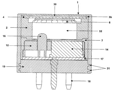
Figure 1 shows the sensor in exploded form; and,
Figure 2 is a cross section of the sensor in its fully
assembled form.
The primary purposes of the design to be described are
to;
(i) maximise the available optical path with a
minimum of reflections within an industry standard "4-
series" housing;
(ii) be simply and easily constructed, (potentially
in an automated process), having a low part count;
(iii) be capable of flameproof certification;
(iv) have low cost .
The favoured design shown in Figures 1 and 2 employs
machined metal parts for the optical housing, the
electronics housing and the outer casing although the use
CA 02546845 2006-05-19
WO 2005/054827 PCT/GB2004/005035
14
of alternative materials is considered later. Metal has
some advantages in terms of ease of certification and in
,even quite significant volumes, there is no cost penalty
over the use of moulded parts. Metal fabrication
techniques other than machining as envisaged here (e. g.
injection metal moulding) could also be employed.
The description applies to sensors for the detection
of CO~ in the 0-5% concentration range, although with
appropriate choice of optical filters and/or different
optical chamber dimensions, different concentration ranges
'and/or gas species (e. g. hydrocarbons) may be detected.
The outer casing 1 is a cylindrical can with gas
diffusion access apertures 5 annularly distributed on its
upper face. The positioning of the apertures is chosen so
that there is adequate space for a gas seal (e.g. via an O
ring or gasket) to be made outside the aperture ring
between the upper face and the casing of an instrument (not
shown) should this be desired. Casing 1 is manufactured
from stainless steel 304 to BS970 and its primary functions
,20 are (a) to protect the internal parts of the sensor; (b)
provide means for gas to access the interior; (c) form (in
conjunction with the internal components) a flame path from
the interior to the exterior, and (d) to provide a key for
the potting compound with which the base of the sensor is
finally sealed. The inner bore of the casing 1 is
toleranced to 18 +0.0/-0.025mm and the thickness of top of
the can is at least 0.4mm to aid machining. The casing is
additionally provided with two annular grooves 31 on the
internal surface near the base into which the potting
compound 19 is keyed on final assembly.
If required, a porous membrane (not shown) of PTFE or
similar material may be applied to the outer or inner plane
surface of the outer casing 1 to help prevent the ingress
of dust, water droplets or liquids.
An optical housing 2 'is cylindrical and is made from
stainless steel 304 to BS 970, additionally provided with
hard acid gold plated 1 micron thick over 2 micron
CA 02546845 2006-05-19
WO 2005/054827 PCT/GB2004/005035
electroless nickel. The part is toleranced to 17.75 +0.025
/-O.Omm to ensure that on assembly (by insertion into outer
casing 1),~ the maximum annular flame path between the two
does not exceed 50 microns, thereby complying with
5 certification requirements. The gold plating ensures that
the internal surface of the component 2, which forms the
upper section of an optical cavity or chamber 32, offers
adequate reflective performance in the IR wavelength. region
of interest (2-6 microns). The main properties required
10 are high reflectivity >95% and long term stability of this
value. The surface may be specularly reflective or diffuse
which would have the advantage of scattering the reflected
radiation and thereby improving its uniformity. IR
reflective coatings other than gold could be employed, and
15 polishing of the inner metal surfaces might also be
acceptable. It is important that the surface is robust and
offers long life without degradation such as might be
caused by corrosion commencing at pinhole imperfections.
The surface may be covered in an IR transparent protective
coating to provide additional reflective efficiency and
assurance. The optical cavity 32 in this case has an
internal diameter of 11.95 +/-0.05mm and a height of 5.5+/-
0.05mm, although even without altering the external
dimensions of the optical housing 2, the internal
dimensions may be varied to some extent, for the purposes
of detecting other gases or to allow different
concentration ranges to be addressed.
In this particular example, therefore, the cavity has
a height to width ratio of approximately 0.46. Cavities of
such dimensions have been found to provide good uniformity
of radiation, resulting in enhanced sensor performance.
However, the cavity could be any shape provided
substantially uniform illumination were achieved.
The optical housing 2 has gas diffusion. access
apertures 6 in its upper face. These are of a number and
distribution such that their disposition relative to
apertures 5 in the outer casing 1 has a minimal effect upon
CA 02546845 2006-05-19
WO 2005/054827 PCT/GB2004/005035
16
the response time of the system. This eases assembly
processes by removing any annular alignment requirement on
the insertion of housing 2 into casing 1. The l.5mm
diameter holes 6 are only half cut into the optical chamber
to maximize the available reflective surface. The region
where the side and top faces of the housing 2 meet tends to
act as a trap for radiation and so contributes
comparatively little to the net throughput from the source
to the detector. Thus, gas access to the sensor may be
through the top face (as preferred by instrumentation
'manufacturers) whilst simultaneously minimizing the impact
of the apertures 6 in reducing the available reflective
surface area.
The optical housing 2 is also required in this example
to retain a flame arresting mesh 4 which is an integral
part of the flameproofing arrangements in the design. The
function of the mesh 4 is to meet the flame transmission
and explosion testing requirements of certification
authorities by arresting any explosion/flame emanating from
within the sensor. In this case we employ one layer of
Dutch twill weave mesh, 0.4mm thick, (Potter & Soar)
although additional layers (or sinter materials) could
readily be incorporated with appropriate dimensional
changes to the assembly. The mesh is retained by peening
into the top face of the optical chamber 2 using a raised
lip (3a in Figure 1) provided for this purpose. In Figure
2, the lip is shown in the assembled position 3b. In
addition to tightly retaining the mesh 4, the resulting lip
also creates a thin mixing chamber 30 around 0.2mm in
height. Gas enters this area after diffusing through the
apertures 5 in the outer casing 1, before passing through
the mesh 4 and entering the optical chamber 32. The
presence of this small void 30 further ensures that there
is minimal dependence of the overall system response time
upon the relative annular orientations of the outer casing
and the optical chamber:
Of course, it will be readily apparent that a sensor
CA 02546845 2006-05-19
WO 2005/054827 PCT/GB2004/005035
17
utilizing uniform radiation, in the manner described, could
be constructed without the components required to achieve
the certification standard. This may be preferable in
situations where only non-combustible gases are to be
detected, for example. In such cases, the sensor may be
built without a flame arrester (mesh 4), and/or there may
be less potting compound.
In this example, the base uses the full available
diameter, the upper optical cavity within the housing 2 has
a slightly~reduced diameter (l2mm as opposed to l5mm).
This reduced diameter does not produce a significant
degradation in behaviour, whilst the smaller surface area
and higher signal levels are beneficial. However, both
versions offer acceptable performance in the intended
application. It will be noted, by reference.to Figure 2,
that the side wall thickness of the housing 2 is
substantially greater than that of the electronics housing
7. This is not essential from a constructional or
certification point of view - both could be made to the
same thickness, which would result in an internal diameter
for the optical cavity of l5mm rather than the nominal l2mm
as shown here. However, as noted, there are some minor
performance advantages (for example the faster filling time
of a smaller gas chamber volume leads to quicker sensor
response/recovery) and no major drawbacks to the approach
chosen.
It should also ~be noted that for gases requiring a
different pathlength, one approach would be to use the l5mm
diameter cavity as discussed above and change the positions
of the source and detector apertures relative to the
central axis. These changes could be achieved with no
external modification to the sensor dimensions and would
still allow certification to be obtained.
An optical IR source 16 and a detector 14 are mounted
on a pcb 17 together with connection pins 18. The source
.in this example is a conventional filament bulb (MG&G 4560
01) although other forms of grey/black body source or solid
CA 02546845 2006-05-19
WO 2005/054827 PCT/GB2004/005035
18
state emitters could also be employed. We have used
pyroelectric detectors in this example (e. g. InfraTec
LIM122 or Perkin Elmer LHi814) provided with appropriate
wavelength selective filters for the target gas of choice,
but semiconductor devices or bolometers are also feasible
alternatives. The detector 14 used here is a two-channel
device, having different wavelength-selective interference
filter windows 15 over each element, in order to create
signal and reference channels. However, single channel
detectors may be employed for uncompensated systems, or
larger numbers of elements can be used to detect multiple
species or provide more sophisticated compensation options.
Also, separate detectors can be used for the signal and
reference channels. A thermistor (e. g. Betatherm
SMD33KF410HT - not shown) may be attached to the pcb 17,
(preferably in close proximity to the detector 14, since
this is the primary source of temperature sensitivity) in
order to provide the temperature data required for thermal
compensation.
In the present design, we have also incorporated an
EEPROM (Dallas D52430AP - not shown) on the pcb 17 in order
' to store information about the sensor and thereby provide
enhanced functionality for the user. In order to minimise
costs, we have not adopted a more sophisticated (but
feasible) approach employing an on board microprocessor to
provide a fully processed sensor output. Since modern
instruments invariably use an external processor to
undertake a multitude of data acquisition, processing and
display functions, we propose that such external processors
perform the necessary calculations. The EEPROM uses
connection pins 18 for communication during the warm-up
period via modulation of a power rail voltage immediately
after power on and requires no dedicated digital
connections. This approach offers designers the maximum
degree of freedom in system integration.
Raw data from the detector channel(s), the thermistor
output, and the relevant coefficients downloaded from
CA 02546845 2006-05-19
WO 2005/054827 PCT/GB2004/005035
19
memory, when externally processed, provide a fully
linearised and temperature compensated output. The EEPROM
may also store other information of relevance (manufacture
date, range, warranty period etc . ) , although the facilities
offered by packages small enough to be integrated within
the sensor housing itself are limited. The ability to
permanently associate information with the sensor within
the flameproof enclosure is a key benefit to users,
especially when undertaking sensor replacements in the
field. It is also possible to configure some of the memory
to allow user-written calibrations or other data to be
stored on board.
A bung 12 fits over the components which protrude from
the pcb 17. PTFE is the preferred material for the bung,
which would normally be moulded; however polypropylene may
be substituted to reduce costs if other constraints permit.
The primary function of the bung 12 is to reduce the free
internal volume of the assembled sensor, since in the
preferred design there are no windows separating the
optical components 14,16 from the gas chamber 32. Without
the bung 12, spaces between and around the source 16 and
detector 14 would gradually become filled with gas on
extended exposure, potentially increasing the response time
of the system. Conversely, gas trapped in these regions
could slowly diffuse back out into the optical path,
thereby increasing the recovery time of the device on
returning to a notionally clean atmosphere. Of course if
windows are provided between the gas chamber 32 and optical
components, close fitting is not necessary.
A further important consideration is that reduction of
the free volume within the sensor significantly reduces the
overpressure which can be generated by an ignition of
combustible gas within the device, and which. the chamber 32
must therefore be able to sustain without damage. This in
turn eases the constraints upon the strength demanded of
.the assembly and allows much more flexibility in the design
of the housing components, and reduces cost and complexity.
CA 02546845 2006-05-19
WO 2005/054827 PCT/GB2004/005035
Bung 12 also fulfils other important purposes. It is
toleranced to provide a close fit around the optical
components 14,16 on the pcb 17, and as such helps to
maintain their alignment and provides protection during
5 assembly processes. It is intended that the bung would be
put in place as soon as the pcb assembly was complete, so
that this component could be shipped with confidence.
Apertures 10 and 11 are provided so that the detector 14
and source 16 are not obscured. The bung 12 also acts as
10 a partial seal to potting compound 19 which might otherwise
'seep into the optical chamber 32 on final assembly of the
device. The seals between the bung 12, detector 14, source
16 and an electronics housing 7 may be formed (for example)
by creating annular flexible features on appropriate
15 surfaces of the bung as part of the moulding process.
Although in the present assembly the ability of the bung to
retain pcb 17 in position after insertion into the
electronics housing 7 is not critical (since no inversion
of the assembly is necessary until after the potting
20 compound 19 has been added and cured), there are other
possible assembly routes in which such additional
functionality of the bung may be of considerable benefit.
The bung may also be provided with a feature 13 which mates
with a locating feature (not shown) on the electronics
housing 7 to ensure that the pcb assembly fits in the
correct orientation. Although this feature could be
omitted in the design shown here (since the bulb can only
protrude into the optical chamber when fitted in the
correct orientation), the presence of an additional keying
feature can help to prevent accidental damage during
assembly.
The bung/pcb assembly fits into the electronics
housing 7 as shown in Figure 2. The electronics housing 7
is manufactured from stainless steel 304, and is provided
with the same gold plating as the optical chamber 2.
Source 16 protrudes through aperture 8 in the upper half of
the housing 7 and into the optical chamber 32 once the
CA 02546845 2006-05-19
WO 2005/054827 PCT/GB2004/005035
21
assembly is complete, whilst the detector windows 15 view
the optical chamber 32 through apertures 9. It should be
noted that it would in fact be preferable, in terms of
approximating the cavity to an ideal integrating sphere, to
position both the source and the detector outside the
cavity. However, for practical reasons it may be necessary
to allow the source envelope to protrude into the cavity
(as in the present embodiment). Such effects should be
minimized wherever possible. The electronics housing 7
provides the plane base reflective surface of the optical
chamber 32, retains the pcb 17 at the correct height and
forms part of the flamepath between the inner and outer
sections of the casing 1 by virtue of the outer diameter
being toleranced to 19.75 +0.025/-O.Omm. Unlike many IR
sensor designs there are no transparent windows to isolate
the source 16 and detector 14 from the gas sample, which
significantly reduces costs and eases assembly. In order
to ensure a good seal between the pcb 17 and electronics
housing 7, a bead of cyanoacrylate adhesive is injected
onto the ledge against which pcb 17 rests in the assembled
device. This provides further insurance against any
leakage of potting compound past this interface.
Flange features at the base of the optical housing 2
and on the top of the electronics housing 7 ensure that the
two mate together correctly, as shown in Figure 2. 3.5mm
of potting compound 19 is applied to the rear of the sensor
to complete the assembly and provide the strength required
to maintain housing integrity in the event of an internal
ignition. Suitable materials are Stycast 2651 or 2850,
manufactured by Emerson Cumming, or Araldite HY956/CW2248.
The overall assembly process therefore consists of a
small number of simple steps
(a) Insert optical housing 2 with attached mesh 4 into
outer casing 1;
(b) Insert populated pcb/bung 17,12 into electronics
housing 7 and seal with adhesive;
(c) Insert electronics housing 7 into outer casing 1 to
CA 02546845 2006-05-19
WO 2005/054827 PCT/GB2004/005035
22
mate with optical housing 2;
(d) Apply potting compound 19 to finally retain all inner
components.
The insertion processes may be performed by hand,
although given the tight tolerances in some cases, a
mechanical press may be useful in preventing binding
between the metal components.
There are a number of alternative approaches to the
materials selected in the above example. Different types of
metal may be used for the optical, electronic and outer
casings, although the requirement for ease of machining and
the demands of certification approvals will limit the
available range. We have also built devices employing
plastic outer casings, and there is no difficulty in
principle in employing all-plastic construction for the
casing, optical and electronic chambers. Suitable
materials are liquid crystal polymer (LCP) or poly
phenylene sulphide (PPS). The required reflective finish
can be produced on plastic, provided that appropriate
processing is employed. A further possibility offered by
the use of plastic parts is the overmoulding of some
components. For example, metal optical surfaces could be
overmoulded to form the outer casing. This has the
advantage of eliminating the flame path which exists
between the inner and outer surfaces in the example here
and might also allow elimination of the potting step.
However, the use of plastic components may affect the
prospects of obtaining flameproof certification.
Different gas species and concentration ranges produce
varying degrees of optical absorption and so may require
significantly different pathlengths for optimum
performance. The use of two parts to create the optical
cavity 32 allows the effective pathlength to be increased
by changing the optical housing 2 (only) to a longer (or
larger diameter) component. Alternatively, placing the
source 16 and detector 14 further towards the perimeter of
the cavity 32 can increase the pathlength. Conversely, the
CA 02546845 2006-05-19
WO 2005/054827 PCT/GB2004/005035
23
pathlength may be reduced by making opposite changes, or by
employing the same optical envelope but reducing the
reflectivity of parts or all of the wall surface. Of
course, such an approach also represents a potential
further deviation from the ideal spherical cavity. For
example, the use of non-reflective (or "blackened")
sections within the cavity might enhance the intensity of
"whispering modes". This could be useful if such modes
were deemed to be an effective means of operation.
Blackening can also be used to "tune" the reflection
characteristics of a cavity. For example, in a cavity
which produces imperfect radiation uniformity, perhaps as
a result of its shape owing to design constraints, well-
positioned blackened portions can improve the uniformity in
certain regions. However, the use of non-reflective
portions needs to be considered carefully and a compromise
reached between enhancement of useful modes and the effect
on the uniformity of the radiation. It will be necessary
to consider the details of the particular sensor design to
determine the effect that blackening will have on its
performance. In general, the ability to introduce such
changes with.only minor modifications to the design is
advantageous when attempting to produce a family of sensors
for different species conforming to a standard package
size.
Electrical connections to and from the sensor are made
via pins 8 in the present example, primarily to maintain
compatibility with existing commercially available devices
and so ease the integration of the improved sensor into
existing instrumentation. However, such connection means
are relatively space inefficient and alternative methods
might be preferable in order to maximize the fraction of
the internal volume available for use as an optical path.
One possible route to achieve this is the use of
overmoulded lead frames to replace some or all of the
.internal pcb and the use of output pads instead of pins.
Direct encapsulation of a lead frame in 'this way can
CA 02546845 2006-05-19
WO 2005/054827 PCT/GB2004/005035
24
produce a highly effective flameproof enclosure.
This design provides a robust optical gas sensing
arrangement, which offers good inter-device reproducibility
and stability against changes affecting the wavelength-
s dependent properties of key components. The sensor is
simply assembled from a small number of components and
requires minimal alignment. It offers pin compatibility
with existing commercial sensors; but also offers access to
valuable extra facilities via the on board EEPROM and
appropriate interrogation circuitry.