Note: Descriptions are shown in the official language in which they were submitted.
CA 02546874 2006-05-23
WO 2005/055460 PCT/US2004/039609
RESONANCE FREQUENCY SHIFT CANCELING
IN WIRELESS HEARING AIDS
Technical Field
This application relates generally to communication systems, and, more
particularly, to systems, devices and methods for canceling a resonance
frequency shift when a wireless communication system, such as those used in
wireless hearing aids, switch between transmit and receive modes.
Background
Some wireless communication systems include a transmit-receive switch,
hereinafter referred to as a TR switch, to transmit arid receive signals using
the
same antenna. Examples of such wireless communications include magnetic
field based communication systems (also referred to herein as inductive
communication systems) having a single inductive coil. In a transmit mode, the
inductive coil is energized to transmit a signal through a resulting time-
varying
magnetic field. In a receive mode, the inductive coil induces a voltage when
in
the presence of a time-varying magnetic field that is representative of a
signal
contained in the field.
Preferably, the frequency of the time-varying magnetic field for a
transmitted signal closely corresponds with the resonant frequency of the
transmitting circuit. A strong signal is transmitted from the antenna by
energizing the coil with a large current at the resonant frequency. The
receiving
circuit has a resonant frequency that corresponds to the frequency of the time-
varying magnetic field that contains the signal to be received.
Unfortunately, the TR switch introduces a resonance frequency shift by
switching the antenna between driving circuitry for a transmit mode and
receiving circuitry for a receive mode. This shift is attributable to the
input
capacitance of a low noise amplifier (LNA), which is also referred to herein
as a
DC blocking capacitor to the LNA. The DC bloclc capacitor forms part of the
resonance frequency in the transmit mode and does not form part of the
resonance frequency in the receive mode. Furthermore, in the transmit mode,
the large current used to drive the coil shifts the value of the coil
inductance in a
CA 02546874 2006-05-23
WO 2005/055460 PCT/US2004/039609
manner that adds to the resonance frequency shift attributable to the DC
blocl~ing capacitor. The resonance frequency shift penalizes the range between
the transmitter and receiver because of the reduced power transfer associated
with the frequency mismatch between the transmitting and receiving devices.
There is a need in the art to provide improve wireless communication
systems.
Summary
The above-mentioned problems are addressed by the present subject
matter and will be understood by reading and studying the following
specification. Various aspects and embodiments of the present subject matter
cancel or otherwise compensate for the frequency shift that occurs when the
hearing aid switches between the transmit and receive modes. The frequency
shift occurs because the LNA input capacitance, also referred to herein as a
DC
blocl~ing capacitor, significantly contributes to the resonance frequency in
the
transmit mode and does not significantly contribute to the resonance frequency
in the receive mode. One embodiment for canceling the resonance frequency
involves adding a capacitor in parallel to the tuning capacitor in the receive
mode. Another embodiment for canceling the resonance frequency involves
adding a capacitance in series in the transmit mode. Another embodiment for
canceling the resonance frequency involves using a center-tapped coil as the
inductive coil of the anterma, where part of the windings are used in the
transmit
mode and all of the windings are used in the receive mode.
Various aspects of the present subject matter relate to a communication
system. Various embodiments of the communication system include an antenna
with a resonant circuit having an inductive coil connected to a tuning
capacitor.
The cormnunication system includes means to selectively drive the resonant
circuit during a transmit mode, and means to selectively~receive an induced
signal in the resonant circuit during a receive mode. The communication system
further includes means to selectively include a frequency shift canceling
component in the resonant circuit to provide a first resonance frequency in
the
resonant circuit in the transmit mode and a second resonance frequency in the
resonant circuit in the receive mode such that the first resonance frequency
and
the second resonance frequency are approximately equal.
CA 02546874 2006-05-23
WO 2005/055460 PCT/US2004/039609
Various aspects of the present subject relate to a hearing aid. Various
embodiments of the hearing aid include a hearing aid receiver to present sound
to an ear, a microphone system to receive acoustic signals, and an antenna
element to transmit and receive inductive signals. The antenna element
includes
a first terminal, a second terminal and a node, and further includes a
resonant
circuit. The resonant circuit includes an inductive coil connected between the
first terminal and the node, and a tuning capacitor connected between the
second
terminal and the node. The hearing further includes a DC blocking capacitor
connected to the node of the antenna element, a frequency shift canceling
component, and signal processing circuitry. The signal processing circuitry is
connected to the microphone system to process received acoustic signals and
present the processed signals to the hearing aid receiver, and is connected to
the
antenna element to process the received inductive signals. The signal
processing
circuitry includes a transmit-receive (TR) switch that responds to a control
signal
to include the frequency shift canceling component in the resonant circuit
when
switching to a first one of the transmit and receive modes, and to exclude the
frequency shift canceling component in the resonant circuit when switching to
a
second one of the transmit and receive modes.
Various aspects relate to a method for switching modes in a wireless
communication system having a resonant circuit in an antenna element.
According to various embodiments of the method, it is determined whether a
trigger to switch modes has occurred. A frequency shift canceling component is
selectively incorporated in the resonant circuit to compensate for a resonant
frequency shift. In various embodiments, the frequency shift canceling
component is incorporated in the resonant circuit to switch from a transmit
mode
to a receive mode. In various embodiments, the frequency shift canceling
component is incorporated in the resonant circuit to switch from a receive
mode
to a transmit mode.
This Summary is an overview of some of the teachings of the present
application and not intended to be an exclusive or exhaustive treatment of the
present subject matter. Further details about the present subject matter are
found
in the detailed description and appended claims. Other aspects will be
apparent
to persons skilled in the art upon reading and understanding the following
detailed description and viewing the drawings that form a part thereof, each
of
CA 02546874 2006-05-23
WO 2005/055460 PCT/US2004/039609
which are not to be taken in a limiting sense. The scope of the present
invention
is defined by the appended claims and their equivalents.
Brief Description of the Drawings
FIG. 1 illustrates a hearing aid device, according to various embodiments
of the present subject matter.
FIG. 2 illustrates a hearing aid device, according to various embodiments
of the present subject matter.
FIG. 3 illustrates portions of a hearing aid device, including a TR switch
for an antenna element, according to various embodiments of the present
subject
matter.
FIG. 4 illustrates the TR switch and the antenna element of FIG. 3,
according to various embodiments of the present subject matter.
FIGS. 5A and SB are schematic illustrations of the antenna element and a
portion of the TR switch of FIG. 4.
FIG. 6 illustrates a simplified circuit schematic for the antenna element
of FIGS. 5A and SB during a transmit mode.
FIGS. 7A and 7B illustrate simplified circuit schematics for the antenna
element of FIGS. 5A and SB during a receive mode.
FIGS. 8A and 8B are schematic illustrations of the antenna element and a
portion of the TR switch, according to a parallel capacitance embodiment of
the
present subject matter.
FIGS. 9A and 9B illustrate simplified circuit schematics for the antenna
element of FIGS. 8A and 8B during a transmit mode, according to various
embodiments of the present subj ect matter.
FIGS. 10A and lOB illustrate simplified circuit schematics for the
antenna element of FIGS. 8A and 8B during a receive mode, according to
various embodiments of the present subject matter.
FIG. 11 is a schematic illustration of the antenna element and a portion of
the TR switch, according to a series capacitance embodiment of the present
subj ect matter.
FIGS. 12A and 12B illustrate simplified circuit schematics for the
antenna element of FIG. 11 during a transmit mode, according to various
embodiments of the present subject matter.
4
CA 02546874 2006-05-23
WO 2005/055460 PCT/US2004/039609
FIGS. 13A and 13B illustrate simplified circuit schematics for the
antenna element of FIG. 11 during a receive mode, according to various
embodiments of the present subject matter.
FIG. 14 is a schematic illustration of the antenna element and a portion of
the TR switch, according to a center-tapped inductor embodiment of the present
subject matter.
FIGS. 15A and 15B illustrate simplified circuit schematics for the
antenna element of FIG. 14 during a transmit mode, according to various
embodiments of the present subject matter.
FIGS. 16A and 16B illustrate simplified circuit schematics for the
antenna element of FIG. 14 during a transmit mode, according to various
embodiments of the present subject matter.
FIGS. 17A, 17B, 17C and 17D illustrate a process for switching
communication modes in a wireless hearing aid, according to various
embodiments of the present subject matter.
Detailed Description
The following detailed description of the present subject matter refers to
the accompanying drawings which show, by way of illustration, specific aspects
and embodiments in which the present subject matter may be practiced. These
embodiments are described in sufficient detail to enable those skilled in the
art to
practice the present subject matter. Other embodiments may be utilized and
structural, logical, and electrical changes may be made without departing from
the scope of the present subject matter. References to "an", "one", or
"various"
embodiments in this disclosure are not necessarily to the same embodiment, and
such references contemplate more than one embodiment. The following detailed
description is, therefore, not to be taken in a limiting sense, and the scope
of the
present subject matter is defined only by the appended claims, along with the
full
scope of legal equivalents to which such claims are entitled.
FIG. 1 illustrates a hearing aid device, according to various embodiments
of the present subject matter. The illustrated hearing aid device 100 is an in-
the-
ear hearing aid that is positioned completely in the ear canal 101. The
present
subj ect matter is not so limited, however. In addition to the illustrated in-
the-ear
style, the features of the present subject matter can be used in other styles
of
hearing assistance devices, including half shell, in-the-canal, behind-the-
ear,
5
CA 02546874 2006-05-23
WO 2005/055460 PCT/US2004/039609
over-the-ear, eyeglass mount, implants, and body worn hearing aids, and
further
can be used in noise-protection earphones, headphones, and the like. Hearing
aids, as used herein, refer to any device that aids a person's hearings, for
example, devices that amplify sound, devices that attenuate sound, and devices
that deliver sound to a specific person such as headsets for portable music
players or radios.
Furthermore, the present subj ect matter provides advantages for other
wireless communications systems that use a single anteima element and a TR
switch to configure the antenna to transmit a signal or receive a signal
without
requiring additional, relatively large and costly electronic components such
as
capacitors. Thus, the present subject matter is useful in efforts to further
miniaturize and reduce costs of wireless communications systems.
Referring again to FIG. 1, a wireless communcation system in the
hearing aid 100 is adapted to communicate with one or more devices. In various
embodiments, the hearing aid 100 uses a magnetic field based wireless
communication system to communicate with an external programmer 102. The
programmer is able to adjust the hearing aid settings such as mode, volume and
the like, to download a complete hearing aid program, and to receive data from
the hearing aid for diagnostics, reporting and the like.
According to various embodiments, the wireless communication system
is based on a magnetic principle that uses a Garner frequency and amplitude
modulation. Various embodiments implement a Garner frequency of
approximately 4 MHz. However, other frequencies can be used as the carrier
frequency. Various embodiments modulate using on/off keying, where the
carrier is ON for a digital "1" and is OFF for a digital "0." In ouoff
lceying, ON
corresponds to approximately 100% of the amplitude and OFF corresponds to
approximately 0% of the amplitude. In one example of another amplitude
modulation technique, a digital "1" corresponds to 100% of the amplitude and a
digital "0" corresponds to 50% of the amplitude. Other amplitude modulation
techniques can be used to transmit the digital data, and thus are within the
scope
of the present subject matter. Thus, embodiments of the wireless communication
system include a digital system which converts an analog signal to a digital
signal. The system has a limited bandwidth. Thus, the digital system further
encodes and compresses the digital signal for transmission.
CA 02546874 2006-05-23
WO 2005/055460 PCT/US2004/039609
In various embodiments, the hearing aid 100 uses a magnetic field based
wireless communication system to communicate with an induction assisted
listening system 104A. In various embodiments, the hearing aid 100 uses a
magnetic field based wireless communication system to communicate with a
device that provides encoded and compressed audio 104B. In various
embodiments, the hearing aid 100 uses a magnetic field based wireless
communication system to communicate with a remote control device 104C.
In various embodiments, the hearing aid 100 uses a magnetic field based
wireless communication system to communicate with another hearing aid 105.
FIG. 2 illustrates a hearing aid, according to various embodiments of the
present subject matter. A wearer is capable of wearing the hearing aid device
200 to aid hearing in an ear. In the illustrated embodiment, the hearing aid
device 200 is adapted to receive acoustic signals 212 (such as speech or other
sound) from an acoustic source 213, and further is adapted to receive a signal
214 from a telecoil transmitter 215. The acoustic source 213 is a source of
sound, as normally perceived by an ear such as a person talking and the like.
Examples of telecoil transmitters 215 include, but are not limited to,
telephones
and some types of programmers.
The environment of the illustrated system includes inductive devices)
216. Examples of induction devices 216 include programmers for hearing aids,
and other hearing aid devices. The present subject matter is not limited to
any
particular type of inductive devices) 216. The hearing aid 200 and the
inductive
devices(s) 216 communicate with each other through a modulated magnetic field
217A and 217B. In general, the inductive devices) 216 include an antenna
element 218 for use to receive signal 217A and transmit signal 217B. The
signal
representative of the received signal 217A is amplified using an amplifier
219, is
demodulated using a demodulator 220 and is provided to signal processor 221.
The signal processor 226 provides various signal processing functions which,
according to various embodiments, include noise reduction, amplification,
frequency response, and/or tone control. A signal representative of a signal
to be
transmitted to the hearing aid 200 is transmitted from the signal processor
221, is
modulated using a modulator 222, and is driven to the antennal element using a
driver 223. The inductive devices) further include application dependent
circuitry 224.
CA 02546874 2006-05-23
WO 2005/055460 PCT/US2004/039609
In the illustrated embodiment, the hearing aid device 200 includes a
hearing aid receiver 225 (or speaker), a signal processor 226, a microphone
system 227 for use to receive acoustic signals 212, a telecoil system 228 for
use
to receive signal 214 from a telecoil transmitter 215, and an antenna element
234
for use to transmit and receive inductive signals 217A and 217B. The
microphone system 227 is capable of detecting the acoustic signal 212 and
providing a representative signal to the signal processing circuit 227. The
telecoil system 228 is capable of receiving a signal 214 from the telecoil
transmitter 215 and providing a representative signal to the signal processor
226.
The hearing aid 200 in the illustrated embodiment further includes a modulator
230 and driver 231, which in conjunction with the antenna element 234, is used
to transmit signal 217A (an amplitude modulated inductive signal at a carrier
frequency to transmit digital data) from the hearing aid 200 to the inductive
devices) 216. The hearing aid 200 in the illustrated embodiment further
includes an amplifier 232 and a demodulator 233, which in conjunction with the
antenna element 234, is used to receive signal 217B (an amplitude modulated
inductive signal at a carrier frequency to transmit digital data) and provide
a
representative signal to the signal processor 226.
The illustrated hearing aid is capable of performing a number of
functions. Some of these functions are identified here as examples. These
examples are not intended to be an exhaustive list of the functions of the
hearing
aid. The wearer of the illustrated hearing aid 200 is capable of programming
the
volume (the amplitude of signal to the receiver 225) while listening to a
person
talking and/or any other acoustic signal 212. Additionally, the hearing aid
200 is
capable of receiving digital audio through signal 217B that can be heard by
the
wearer of the hearing aid 200 without the acoustic sound or that can be
superimposed with representative acoustic signals such that both the acoustic
sound and the digital audio are heard by the wearer of the hearing aid 200.
One of ordinary slcill in the art will understand that the antenna element
217 is an RLC circuit that has a resonant frequency. RLC circuits include a
resistive (R), an inductive (L) and a capacitive (C) component. Each of the
components are capable of being formed from one or more discrete elements.
For example, the resistive (R) component includes inherent resistance in the
signal pathways and in the devices, the inductive (L) component includes the
CA 02546874 2006-05-23
WO 2005/055460 PCT/US2004/039609
inductance associated with the inductive coil in the antenna element, and the
capacitive component includes the capacitance associated with the tuning
capacitor, the DC blocl~ing capacitor in the receive mode, and various
parasitic
capacitances.
The present subject matter cancels the frequency shift that occurs when
the hearing aid switches between transmit and receive modes. As will be shown
with respect to FIGS. 3, 4, SA, SB, 6, 7A and 7B, the frequency shift occurs
because an LNA input capacitance, also referred to herein as a DC blocking
capacitor, significantly contributes to the resonance frequency in the
transmit
mode and does not significantly contribute to the resonance frequency in the
receive mode
One embodiment of the present subject matter compensates for the
resonance frequency shift by adding capacitance in parallel to the tuning
capacitor in the receive mode. Another embodiment of the present subject
matter compensates for the resonance frequency shift by adding capacitance in
series in the transmit mode. Another embodiment of the present subject matter
compensates for the resonance frequency shift by using part of the windings of
a
center-tapped coil in the transmit mode and all of the windings of the center-
tapped coil in the receive mode.
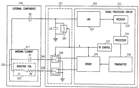
FIG. 3 illustrates portions of a hearing aid device, including a TR switch
for an antenna element, according to various embodiments of the present
subject
matter. The illustration includes representations for an integrated circuit
(IC)
portion 329 and for external components 315 with respect to the IC portion.
The
IC portion 329 includes the signal processing circuit 315 and a TR switch 331.
The external components 315 include the antenna element 317. The
antenna element includes an inductive coil 332, represented by an inductor L1
in
series with a resistance R1 associated with the resistance in the coil. The
resistance Rl can also represent other resistances, such as the resistance in
the
lines or current limiting resistors. The antenna element 317 also includes a
tuning capacitor C1 connected to the inductive coil at a node 333, also
referred
to as a center point, center node or signal pickup node. When the antenna
element 317 receives a signal from an inductive source, a voltage is induced
at
the node 333. This voltage is presented to a low noise amplifier 354 in the IC
329 through a DC bloclcing capacitor C2. The voltage of a received signal
CA 02546874 2006-05-23
WO 2005/055460 PCT/US2004/039609
applied to the input of the amplifier 354 is in the microvolt to minivolt
range,
and thus will not damage the IC 329. However, the voltage at the node 333 is
several time higher than a maximum IC voltage rating (depending on the Q-
factor) when a current is driven through the inductive coil 332 to transmit a
signal from the antenna element 317. As is described in detail below, aspects
of
the present subject matter provides means to protect the IC from this high
voltage.
The illustrated IC 329 includes a low noise amplifier 354 to receive an
induced signal from the antenna element 317, and a driver 352 to drive a
current
through the inductive coil 332 of the antenna element 317 and transmit an
inductive signal from the antenna element. The illustrated IC signal
processing
circuit 315 further includes a processor 334 in communication with a receiver
335 to process received signals from the amplifier 354, and in communication
with a transmitter 336 to present a signal to the driver 352 that is to be
driven
through the inductive coil 332 of the antenna element 317. The illustrated
signal
processing circuit includes a TR control 337 to enable the driver, and to
appropriately actuate the TR switch 331 to either transmit signals to the
antenna
element 333 in a transmit mode or receive signals from the antenna element 333
in a receive mode.
The illustrated TR switch functions to configure the antenna element 317
in series in the transmit mode and in parallel in the receive mode, and
further
functions to protect the IC from the large voltages generated at the node 333
during the transmit mode by shunting a capacitance C3 associated with the IC.
A first portion 338 of the TR switch 331 is responsive to the TR control
signal to
operatively connect the driver 352 to the antenna element 317 during the
transmit mode, and connect a first terminal 339 of the antemla element to a
second terminal 340 of the antenna element to place the tuning capacitor C1 in
parallel with the inductive coil 332 during the receive mode. In various
embodiments, the first and second terminals 339 and 340 of the antenna element
are connected to ground during the receive mode. A second portion 341 of the
TR switch 331 is responsive to the TR control signal to form a shunt across
the
IC capacitance C3 to protect the IC during the transmit mode. One of ordinary
skill in the art will understand, upon reading and comprehending the
disclosure
below, that additional portions of the TR switch are used to selectively
include
to
CA 02546874 2006-05-23
WO 2005/055460 PCT/US2004/039609
or exclude a frequency canceling component, according to various embodiments
of the present subject matter.
FIG. 4 illustrates the TR switch and the antenna element of FIG. 3,
according to various embodiments of the present subject matter. In various
embodiments, the first portion 438 of the TR switch 431 includes a first and
second pass transistors 442 and 443 to selectively connect the driver to the
antenna element during the transmit mode, and further includes a first and
second pull-down transistors 444 and 445 to selectively ground the first and
second terminals 439 and 440 of the antenna element during the receive mode.
The gates of the first and second pass transistors and the first and second
pull-
down transistors are appropriately connected to the TR control signal to
perform
the desired function. The illustrated first portion of the TR switch is an
embodiment, and is not intended to be the only design for a TR switch. Those
of
ordinary skill in the art will appreciate, upon reading and comprehending this
disclosure, that there are other circuits that can be designed to perform the
function of the first portion of the TR switch. Other circuits are capable of
selectively connecting the driver to the antenna so that the components of the
antenna are in series, and are capable of selectively disconnecting the driver
from the antenna and connecting the tuning capacitor C1 in parallel across the
inductive coil 432. W various embodiments, the second portion 441 of the TR
switch 431 includes a bypass transistor 446 connected across the IC
capacitance
C3. The gate of the bypass transistor is appropriately connected to the TR
control to perform the desired function. In various embodiments, the TR switch
431 includes a third portion 447 used to selectively include or exclude a
frequency canceling component 448, according to various embodiments of the
present subject matter. The third portion of the TR switch 431 and the
frequency
canceling component 448 are generally illustrates. Various embodiments of the
frequency canceling component 448 include an external or non-IC components
and various embodiments of the frequency canceling component 448 include an
IC component.
The basic resonant circuit with the TR switch has a problem with
resonant frequency shift when the mode changes from transmit to receive or
from receive to transmit. There are two contributors to this shift, and both
contributing factors add rather than cancel each other. The first contributing
11
CA 02546874 2006-05-23
WO 2005/055460 PCT/US2004/039609
factor involves the changing inductance of the coil caused by the change in
magnetic permeability of the fernte core as the current drive level changes
between transmit and receive mode. It is noted that this contributing factor
is not
an issue for air coils because the magnetic permeability is constant for air
and is
independent of the drive level. The second contributing factor is the DC
bypass
capacitor C2, which is part of the resonance circuit in the transmit mode.
However, the DC bypass capacitor C2 is almost eliminated in the receive mode
by the parasitic capacitance C3, which is much smaller than C2 and C1.
FIGS. 5A and SB are schematic illustrations of the antenna element and a
portion of the TR switch of FIG. 4. These illustrations doe not include a
frequency canceling component. The antenna element includes the inductive
coil 532 (L1 and R1) and the tuning capacitor C1. A first terminal 539 of the
antemla element is connected to the inductive coil, and a second terminal 540
of
the antenna element is connected to the tuning capacitor C1. The tuning
capacitor C1 is connected to the inductive coil at a node 533 of the antenna
element. The node 533 is connected to an input (LNA INPUT) of the low noise
amplifier via the DC blocking capacitor C2. The input of the amplifier is
associated with an IC capacitance C3. A bypass transistor M1, illustrated in
FIG. 4 as 441, is connected across the IC capacitance, and is responsive to a
TR
control signal to selectively pull the amplifier input to ground to protect
the IC
from the high voltages generated at the node of the antenna element when a
current is driven through the inductive coil. The schematic illustrated in
FIG. 5B
rearranges the components of the schematic in FIG. 5A to provide a schematic
layout similar to the layout used in FIGS. 6, 7A and 7B to analyze the
circuit.
FIG. 6 illustrates a simplified circuit schematic for the antenna element
of FIGS. 5A and SB during a transmit mode. Terminals 639 and 640, coil 632
and node 633 generally correspond to terminals 539 and 540, coil 532 and node
533 in FIG. 5, and to terminals 339 and 340, coil 332 and node 333 in FIG. 3.
During the transmit mode, transistor M1 is actuated to provide a shunt across
the
IC capacitance C3. The illustrated resistance RM1 represents the on-resistance
of
transistor M1. The value of RMl is relatively small, and thus can be ignored
for
the purposes of this discussion. The tuning capacitor C1 and the DC bypass
capacitor C2 are effectively connected in parallel such that the equivalent
12
CA 02546874 2006-05-23
WO 2005/055460 PCT/US2004/039609
capacitance of C1 and C2 is C1 + C2. Thus, in the transmit mode, the resonance
frequency for the antenna element of FIG. 5 is provided by Equation 1.
(1) fTx - 1 TX MODE, NO CANCELING
2~t Ll x (C1 + C2)
FIGS. 7A and 7B illustrate simplified circuit schematics for the antenna
element of FIGS. 5A and SB during a receive mode. Terminals 739 and 740,
coil 732 and node 733 generally correspond to terminals 539 and 540, coil 532
and node 533 in FIG. 5, and to terminals 339 and 340, coil 332 and node 333 in
FIG. 3. During the receive mode, transistor M1 is not actuated and the driver
terminals are pulled to a reference potential (e.g. ground). As illustrated in
FIG.
7A, the DC bypass capacitor C2 and the IC capacitance C3 are connected in
series (represented as C2 // C3, which corresponds to C2*C3 / (C2 + C3)). The
IC capacitance C3 is much smaller than the DC bypass capacitance C2. Thus,
the equivalent capacitance for C2 and C3 is sufficiently small such that they
can
be ignored for the purpose of this discussion. Therefore, in the receive mode,
the
antenna circuit can be further simplified as shown in FIG. 7B. FIGS. 7A and 7B
also indicate that, in the receive mode, the inductance of L1 has been reduced
by
0L due to the change in current through the coil L1, which changes the
magnetic
permeability of the ferrite core of the coil. One of ordinary skill in the art
will
understand, upon reading and comprehending this disclosure, that the magnetic
permeability for an air coil is constant and independent of the current, and
thus
will not affected by inductance change ~L.
In the receive mode, the resonance frequency for the antenna element of
FIG. 5 is provided by Equation 2, where 0L is the inductance change
attributable
to the absence of the drive current.
(2) f~ = 1 RX MODE, NO CANCELING
2~t (L1 - DL) x Cl
It is clear from Equations 1 and 2 that both the capacitance and the
inductance decrease in the receive mode, such that the resonant frequency in
the
receive mode is higher than the resonant frequency in the transmit mode. The
13
CA 02546874 2006-05-23
WO 2005/055460 PCT/US2004/039609
present subject matter selectively incorporates a frequency shift canceling
component to compensate for the change in resonant frequency when switching
from the transmit mode to the receive mode, and from the receive mode to the
transmit mode.
The present subject matter cancels out the frequency shift that occurs
when the hearing aid toggles between the transmit and receive modes. FIGS.
8A, 8B, 9A, 9B, 10A and l OB, described below, illustrate the circuit of FIGS.
5A and 5B where a capacitance is selectively added in parallel with respect to
the tuning capacitor. FIGS. 1 l, 12A, 12B, 13A and 13B, described below,
illustrate the circuit of FIGS. 5A and 5B where a capacitance is selectively
added
in series with respect to the tuning capacitor. FIGS. 14, 15A, 15B, 16A and
168, described below, illustrate the circuit of FIG. 5 where a center-tapped
coil
is used as the inductive coil in the antenna, and the circuit is configured to
selectively increase inductance in the receive mode and decrease inductance in
the transmit mode.
Parallel C~acitor Embodiment
FIGS. 8A and 8B are schematic illustrations of the anteima element and a
portion of the TR switch, according to a parallel capacitance embodiment of
the
present subj ect matter. The illustrated circuit is similar to the circuit
illustrated
in FIGS. 5A and 5B, and further includes frequency shift canceling components.
These components include capacitor C4 and transistor M2. Terminals 839 and
840, coil 832 and node 833 generally correspond to terminals 539 and 540, coil
532 and node 533 in FIG. 5, and to terminals 339 and 340, coil 332 and node
333 in FIG. 3.
Capacitor C4 and transistor M2 are connected in series from the node
833 of the antenna element to the reference potential (e.g. ground). One of
ordinary slcill in the art will understand, upon reading and comprehending
this
disclosure, that the capacitor C4 and transistor M1 are effectively connected
in
parallel across the tuning capacitor C1 during the receive mode when the
driver
terminals are pulled to a reference potential (e.g. ground). Transistor M2 has
a
parasitic capacitance, illustrated as capacitor C5. Transistor M2 functions as
a
switch under control of the TR Mode signal. Thus, transistor M2 can be
considered to be the third portion 447 of the TR switch 431 and capacitor C4
can
14
CA 02546874 2006-05-23
WO 2005/055460 PCT/US2004/039609
be considered to be the frequency canceling component 448 illustrated in FIG.
4.
In the illustrated embodiment, transistor M1 is actuated during a transmit
mode,
and transistor M2 is actuated during a receive mode.
FIGS. 9A and 9B illustrate simplified circuit schematics for the antenna
element of FIGS. 8A and 8B during a transmit mode, according to various
embodiments of the present subject matter. Terminals 939 and 940, coil 932 and
node 933 generally correspond to terminals 539 and 540, coil 532 and node 533
in FIG. 5, and to terminals 339 and 340, coil 332 and node 333 in FIG. 3. In
the
transmit mode, transistor M1 is actuated and transistor M2 is not actuated.
FIG.
9A illustrates transistor M1 with resistance RMI, which represents the on-
resistance of transistor Ml, and further illustrates transistor M2 with its
parasitic
capacitance C5. The parasitic capacitance C5 and capacitor C4 are connected in
series (represented as C4 // C5, which corresponds to C4*C5 / (C4 + CS)). The
capacitance C4 is selected to be much larger than the parasitic capacitance
C5.
Thus, as indicated in the schematic of FIG. 9B, the equivalent capacitance for
the combination of C4 and C5 is sufficiently small such that they can be
ignored
for the purpose of this discussion. Furthermore, the relatively small on-
resistance of transistor M1 (RMl) can also be ignored for the purpose of this
discussion. FIG. 9B illustrates a simplified schematic of the antenna element
of
FIGS. 8A and 8B during the transmit mode.
From FIG. 9B, the resonance frequency in the transmit mode is
represented by Equation 3.
(3) f~ - 1 TX MODE, PARALLEL
27C' L1 x (C1 + C2)
Thus, as is evident from Equation 3, the tuning capacitor Cl and the DC bypass
capacitor C2 are substantive elements for determining the resonance frequency
in the transmit mode for the illustrated parallel capacitor embodiment.
FIGS. 10A and lOB illustrate simplified circuit schematics for the
antenna element of FIGS. 8A and 8B during a receive mode, according to
various embodiments of the present subject matter. During the receive mode,
transistor M1 is not actuated, transistor M2 is actuated, and the driver
terminals
are pulled to a reference potential (e.g. ground). FIG. 10A illustrates
transistor
CA 02546874 2006-05-23
WO 2005/055460 PCT/US2004/039609
Ml with its parasitic capacitance C3, which is also representative of the IC
capacitance, and transistor M2 with its on-resistance RMZ. The IC capacitance
C3 and the DC bypass capacitor C2 are connected in series (represented as C2
//
C3, which coiTesponds to C2*C3 / (C2 + C3)). The capacitance C2 is selected
to be much larger than the parasitic capacitance C3. Thus, as indicated in the
schematic of FIG. l OB, the equivalent capacitance for C2 and C3 is
sufficiently
small such that they can be ignored for the purpose of this discussion.
Furthermore, the relatively small on-resistance of transistor M2 (RM2) can
also
be ignored for the purpose of this discussion. FIG. l OB illustrates a
simplified
schematic of the antenna element of FIGS. 8A and 8B during the receive mode.
In the receive mode, the inductance of L1 has been reduced by 0L due to the
change in current through the coil Ll, which changes the magnetic permeability
of the ferrite core of the coil.
From FIG. 10B, the resonance frequency in the receive mode is
represented by Equation 4.
(4) f~ - 1 RX MODE, PARALLEL
2~c (L1 - t~L) x (C1 + C4)
Thus, as is evident from Equation 4, the tuning capacitor C1 and the
additional
capacitor C4 are substantive elements for determining the resonance frequency
in the receive mode for the illustrated parallel capacitor embodiment. C4 is
selected to compensate for both missing capacitance attributed to the DC
bypass
capacitor C2 and the lower inductance 0L attributable to the absence of the
transmitting drive current. C4 is larger than C2 to cancel the frequency shift
caused by C2 and L1. This solution eliminates the frequency shift with one
additional capacitor.
Series Capacitor Embodiment
FIG. 11 is a schematic illustration of the antenna element and a portion of
the TR switch, according to a series capacitance embodiment of the present
subject matter. The illustrated circuit is similar to the circuit illustrated
in FIGS.
5A and SB, and further includes frequency shift canceling components. These
components include capacitor C6 and transistor M3. Terminals 1139 and 1140,
16
CA 02546874 2006-05-23
WO 2005/055460 PCT/US2004/039609
coil 1132 and node 1133 generally correspond to terminals 539 and 540, coil
532
and node 533 in FIG. 5, and to terminals 339 and 340, coil 332 and node 333 in
FIG. 3.
Capacitor C6 is connected in series with the coil and the tuning capacitor
C1. Transistor M3 is connected to pull node 1149 to a reference potential
(e.g.
ground) during a receive mode. One of ordinary skill in the art will
understand,
upon reading and comprehending this disclosure, that the capacitor C6 is
effectively connected in series with respect to the tuning capacitor Cl during
the
transmit mode. Transistor M3 has a parasitic capacitance, illustrated as
capacitor
C7. Transistor M3 functions as a switch under control of the TR Mode signal.
Thus, transistor M3 can be considered to be the third portion 447 of the TR
switch 431 and capacitor C6 can be considered to be the frequency canceling
component 448 illustrated in FIG. 4. In the illustrated embodiment, transistor
Ml is actuated during a transmit mode, and transistor M3 is actuated during a
receive mode.
FIGS. 12A and 12B illustrate simplified circuit schematics for the
anteima element of FIG. 11 during a transmit mode, according to various
embodiments of the present subject matter. Terminals 1239 and 1240, coil 1232
and node 1233 generally correspond to terminals 539 and 540, coil 532 and node
533 in FIG. 5, and to terminals 339 and 340, coil 332 and node 333 in FIG. 3.
In
the transmit mode, transistor M1 is actuated and transistor M3 is not
actuated.
FIG. 12A illustrates transistor M1 with resistance RMI, which represents the
on-
resistance of transistor M1, and further illustrates transistor M3 with its
parasitic
capacitance C7. The parasitic capacitance C7 is insignificant for the purposes
of
this discussion. Thus, as indicated in the schematic of FIG. 10B, the
capacitor is
illustrated in series with the parallel combination of tuning capacitor C1 and
the
DC bypass capacitor.. Furthermore, the relatively small on-resistance of
transistor M1 (RMl) can also be ignored for the purpose of this discussion.
FIG.
12B illustrates a simplified schematic of the antenna element of FIGS. 11A and
11B during the transmit mode.
From FIG. 12B, the resonance frequency in the transmit mode is
represented by Equations 5 and 6.
17
CA 02546874 2006-05-23
WO 2005/055460 PCT/US2004/039609
_ 1
fT~ 27C Ll x ((C1 + C2) /l C6) ' or
TX MODE, SERIES
(6) fTx = 1
2~' 1;1 x (C1 + C2) x C6
Cl+C2+C6
Thus, as is evident from Equations 5 and 6, the tuning capacitor C1, the DC
bypass capacitor C2, and capacitor C6 are substantive elements for determining
the resonance frequency in the transmit mode for the illustrated series
capacitor
embodiment.
FIGS. 13A and 13B illustrate simplified circuit schematics for the
antenna element of FIG. 11 during a receive mode, according to various
embodiments of the present subject matter. Terminals 1339 and 1340, coil 1332
and node 1333 generally correspond to terminals 539 and 540, coil 532 and node
533 in FIG. 5, and to terminals 339 and 340, coil 332 and node 333 in FIG. 3.
During the receive mode, transistor M1 is not actuated, transistor M3 is
actuated,
and the driver terminals are pulled to a reference potential (e.g. ground).
FIG.
13A illustrates transistor M1 with its parasitic capacitance C3, which is also
representative of the IC capacitance, and transistor M3 with its on-resistance
RM3. The IC capacitance C3 and the DC bypass capacitor C2 are connected in
series (represented as C2 // C3, which corresponds to C2'kC3 / (C2 + C3)). The
capacitance C2 is selected to be much larger than the parasitic capacitance
C3.
Thus, as indicated in the schematic of FIG. 13B, the equivalent capacitance
for
C2 and C3 is sufficiently small such that they can be ignored for the purpose
of
this discussion. The on-resistance of transistor M3 (RM3) pulls a node of the
coil
to a reference potential (e.g. ground). The value of RM3 is sufficiently small
to
be ignored for the purposes of this discussion. FIG. 13B illustrates a
simplified
schematic of the antenna element of FIG. 11 during the receive mode. In the
receive mode, the inductance of L1 has been reduced by ~L due to the change in
current through the coil L1, which changes the magnetic permeability of the
ferrite core of the coil.
From FIG. 13B, the resonance frequency in the receive mode is
represented by Equation 7.
1s
CA 02546874 2006-05-23
WO 2005/055460 PCT/US2004/039609
f~ - 1 RX MODE, SERIES
2~t (L1 - ~1L) x Cl
Thus, as is evident from Equation 7, the tuning capacitor C1 is a substantive
component for determiiung the resonance frequency in the receive mode for the
illustrated series capacitor embodiment. C6 is selected to compensate for both
missing capacitance attributed to the DC bypass capacitor C2 and the lower
inductance ~L attributable to the absence of the transmitting drive current.
This
solution eliminates the frequency shift with one additional capacitor.
Center-Taped Coil Embodiment
FIG. 14 is a schematic illustration of the antenna element and a portion of
the TR switch, according to a center-tapped inductor embodiment of the present
subj ect matter. The illustrated circuit is similar to the circuit illustrated
in FIGS.
5A and SB, and further includes frequency shift canceling components. These
components include a center-tapped coil Ll, L2 and a transistor M4. Terminals
1439 and 1440, coil 1432 and node 1433 generally correspond to terminals 539
and 540, coil 532 and node 533 in FIG. 5, and to terminals 339 and 340, coil
332
and node 333 in FIG. 3.
One of ordinary skill in the art will understand, upon reading and
comprehending this disclosure, that two separate coils can be used to replace
the
center-tapped coil. Additionally, one of ordinary skill in the art will
understand,
upon reading and comprehending this disclosure, that first coil portion L1 and
the second coil portion L2 of the coil need not have an equal number of turns
or
equal inductance. The term center-tapped coil is intended to include coils
having
a tap anywhere along its length to form the first coil portion L1 and the
second
coil portion L2. Various embodiments wind the first coil portion L1 and the
second coil portion L2 on the same core. One of the driver terminals is
connected to a node 1450 between the first coil portion Ll and the second coil
portion L2.
Transistor M4 is configured to pull the second coil portion L2 to a
reference potential (e.g. ground) during a receive mode. Transistor M4 has a
parasitic capacitance, illustrated as capacitor C8. Transistor M4 fimctions as
a
switch under control of the TR Mode signal. Thus, transistor M4 can be
19
CA 02546874 2006-05-23
WO 2005/055460 PCT/US2004/039609
considered to be the third portion 447 of the TR switch 431 and the second
coil
portion L2 can be considered to be the frequency canceling component 448
illustrated in FIG. 4. In the illustrated embodiment, transistor M1 is
actuated
during a transmit mode, and transistor M4 is actuated during a receive mode.
FIGS. 15A and 15B illustrate simplified circuit schematics for the
antenna element of FIG. 14 during a transmit mode, according to various
embodiments of the present subject matter. Terminals 1539 and 1540, coil 1532
and node 1533 generally correspond to terminals 539 and 540, coil 532 and node
533 in FIG. 5, and to terminals 339 and 340, coil 332 and node 333 in FIG. 3.
In the transmit mode, transistor M1 is actuated and transistor M4 is not
actuated. FIG. 15A illustrates transistor Ml with resistance RMI, which
represents the on-resistance of transistor M1, and further illustrates
transistor M4
with its parasitic capacitance C8. The relatively small on-resistance of
transistor
Ml (RM1) can also be ignored for the purpose of this discussion. In the
transmit
mode, two LC circuits exist simultaneously. The main LC (L1 and C1+C2) and
a parasitic LC (L2 and C which is the pad capacitance). The parasitic
resonance
frequency is more than a decade higher than the driver frequency in order to
avoid magnetic field cancellation in the magnetic core. Also the voltage at
the
node between L2 and C8 is not higher than the drive voltage. FIG. 15B
illustrates a simplified schematic of the antenna element of FIGS. 14A and 14B
during the transmit mode.
From FIG. 15B, the resonance frequency in the transmit mode is
represented by Equation 8.
1 TX MODE, CENTER-TAPPED
(8) f''~ 2~ Ll x (C1 + C2)
Thus, as is evident from Equation 8, the tuning capacitor C1, the DC bypass
capacitor C2 and the first coil portion Ll are substantive components for
determining the resonance frequency in the transmit mode for the illustrated
center-tapped inductor embodiment.
FIGS. 16A and 16B illustrate simplified circuit schematics for the
antenna element of FIG. 14 during a receive mode, according to various
embodiments of the present subject matter. Terminals 1639 and 1640, coil 1632
CA 02546874 2006-05-23
WO 2005/055460 PCT/US2004/039609
and node 1633 generally correspond to terminals 539 and 540, coil 532 and node
533 in FIG. 5, and to terminals 339 and 340, coil 332 and node 333 in FIG. 3.
In the transmit mode, transistor M1 is not actuated and transistor M4 is
actuated. FIG. 16A illustrates transistor M4 with resistance RM4, which
represents the on-resistance of transistor M4, and further illustrates
transistor M1
with its parasitic capacitance C8, which is also representative of the IC
capacitance. The relatively small on-resistance of transistor M4 (RM4) can
also
be ignored for the purpose of this discussion. In the receive mode, the driver
between the first inductive portion L1 and the second inductive portion L2
goes
into tri-state. The parasitic capacitance C9 should be so small that it have a
negligible effect on the receive circuit.
From FIG. 16B, the resonance frequency in the receive mode is
represented by Equation 9.
1 RX MODE, CENTER-TAPPED
(9) .fTx - 2~ Ll - 0L + L2) ~ Cl
Thus, as is evident from Equation 9, the first and second inductive portions
L1 +
L2 and the tuning capacitor Cl are substantive components for determining the
resonance frequency in the receive mode. L2 is large enough to compensate for
the L1 change and L2. This embodiment involves only a few additional turns on
the existing magnetic core. It is also suitable for IC implementation with a
minimal number of external parts. These external parts are L1, L2, Rl, C1 and
C2. Furthermore, the voltages at the IC pads will not be higher than the drive
voltage and therefore, eliminating the rislc of generating voltages higher
than the
maximum rated values.
FIGS. 17A, 17B, 17C and 17D illustrate a process for switching
communication modes in a wireless hearing aid, according to various
embodiments of the present subject matter. Referring to FIG. 17A, a trigger
signal is provided to switch modes, including to switch from a receive mode to
a
transmit mode, and to switch from a transmit mode to a receive mode. At 1760,
it is determined whether a trigger to switch modes has occurred. When a
trigger
to switch modes occurs, the process proceeds to 1761, where a frequency shift
canceling component is appropriately included or excluded for a desired mode
21
CA 02546874 2006-05-23
WO 2005/055460 PCT/US2004/039609
based on a circuit configuration and the desired mode. The frequency shift
canceling component, or components, are used to compensate for the changing
inductance of the coil caused by the change in magnetic permeability of the
fernte core as the current drive level changes between transmit and receive
mode, and the near elimination of the DC bypass capacitor C2 in the receive
mode.
FIG. 17B illustrates a process for switching communication modes in a
wireless hearing aid, according to a parallel capacitor embodiment of the
present
subject matter. In this embodiment, the frequency shift canceling component
includes a parallel capacitance with respect to the tuning capacitor. At 1760,
it is
determined whether a trigger to switch modes has occurred. When a trigger to
switch modes occurs, the process proceeds to 1762, where it is determined
whether the mode is being switched to a transmit mode, represented at 1763, or
to a receive mode, represented at 1764. When the mode is being switched to the
transmit mode 1763, the process proceeds to 1765, where a parallel capacitance
with respect to the tuning capacitor is removed to cancel the frequency shift
associated with switching from the receive mode to 'the transmit mode. When
the mode is being switched to the receive mode 1764, the process proceeds to
1766, where the parallel capacitance with respect to the tuning capacitor is
added
to cancel the frequency shift associated with switching from the transmit mode
to the receive mode.
FIG. 17C illustrates a process for switching communication modes in a
wireless hearing aid, according to a series capacitor embodiment of the
present
subject matter. In this embodiment, the frequency shift canceling component
includes a series capacitance with respect to the tuning capacitor. At 1760,
it is
determined whether a trigger to switch modes has occurred. When a trigger to
switch modes occurs, the process proceeds to 1762, where it is determined
whether the mode is being switched to a transmit mode, represented at 1763, or
to a receive mode, represented at 1764. When the mode is being switched to the
transmit mode 1763, the process proceeds to 1767, where a series capacitance
with respect to the tuning capacitor is added to cancel the frequency shift
associated with switching from the receive mode to the transmit mode. When
the mode is being switched to the receive mode 1764, the process proceeds to
1768, where the series capacitance with respect to the tuning capacitor is
22
CA 02546874 2006-05-23
WO 2005/055460 PCT/US2004/039609
removed to cancel the frequency shift associated with switching from the
transmit mode to the receive mode.
FIG. 17D illustrates a process for switching communication modes in a
wireless hearing aid, according to a center-tapped inductor embodiment of the
present subject matter. In this embodiment, the frequency shift canceling
component includes a removable inductance. At 1760, it is determined whether
a trigger to switch modes has occurred. When a trigger to switch modes occurs,
the process proceeds to 1762, where it is determined whether the mode is being
switched to a transmit mode, represented at 1763, or to a receive mode,
represented at 1764. When the mode is being switched to the transmit mode
1763, the process proceeds to 1769, where inductance is removed to cancel the
frequency shift associated with switching from the receive mode to the
transmit
mode. When the mode is being switched to the receive mode 1764, the process
proceeds to 1770, where inductance is added to cancel the frequency shift
associated with switching from the transmit mode to the receive mode. In
various embodiment that use a center-tapped coil having a first inductive
portion
and a second inductive portion, the frequency shift canceling component
includes the second inductive portion, which is removed from the resonant
circuit during the transmit mode and incorporated in the resonant circuit
during
the receive mode.
One of ordinary skill in the art will understand, upon reading and
comprehending this disclosure, that the present subject matter is capable of
being
incorporated in a variety of near-field communication systems and technology
that use such near-field connnunication systems such as hearing aids. For
example, the present subject mater is capable of being used in hearing aids
such
as in-the-ear, half shell and in-the-canal styles of hearing aids, as well as
for
behind-the-ear hearing aids. Furthermore, one of ordinary shill in the art
will
understand, upon reading and comprehending this disclosure, the method aspects
of the present subject matter using the figures presented and described in
detail
above.
Although specific embodiments have been illustrated and described
herein, it will be appreciated by those of ordinary shill in the art that any
arrangement which is calculated to achieve the same purpose may be substituted
for the specific embodiment shown. This application is intended to cover
23
CA 02546874 2006-05-23
WO 2005/055460 PCT/US2004/039609
adaptations or variations of the present subject matter. It is to be
understood that
the above description is intended to be illustrative, and not restrictive.
Combinations of the above embodiments, and other embodiments will be
apparent to those of shill in the art upon reviewing the above description.
The
scope of the present subject matter should be determined with reference to the
appended claims, along with the full scope of equivalents to which such claims
are entitled.
24