Note: Descriptions are shown in the official language in which they were submitted.
CA 02548312 2006-06-05
WO 2005/064355 PCT/US2004/041479
CHARACTERIZING CIRCUIT PERFORMANCE
BACKGROUND OF THE INVENTION
Field of the Invention
s The invention relates to the field of integrated circuit testing, and in
particular to a system and method for determining the signal delay
contributions
from specific process layers.
'4
Related Art
1o The performance of an integrated circuit (IC) is largely determined by its
timing characteristics (i.e., the speed at which signals propagate through the
IC).
This signal propagation speed is typically analyzed via standalone testing
systems that interface with dedicated test structures formed on the IC chip.
Note
that the term "IC chip" refers to the combination of the IC (i.e., the circuit
1s structures and devices that provide the desired functionality, such as a
field
programmable gate array (FPGA) or an complex programmable logic device
(CPLD)) and the die, or substrate, on which the IC is formed. Because a large
number of IC chips are manufactured simultaneously on a single wafer, the die
area is larger than the IC area, to allow for scribe line regions between ICs.
The
2o scribe line regions allow the wafer to be sawn apart into individual IC
chips
without risk of damage to the ICs.
The scribe line regions also provide locations for the dedicated test
structures used in conventional IC test techniques. For example, Fig. 1 shows
a
conventional IC chip 100 that includes an FPGA 110 formed on a die 120.
25 FPGA 110 includes multiple configurable logic blocks (CLBs) 111, multiple
input/output blocks (IOBs) 112, and a programmable interconnect matrix 113
that routes signals between the CLBs and IOBs. CLBs 111, IOBs 112, and
interconnect matrix 113 are programmable by a user to provide a desired
functionality for IC chip 100.
3o IC chip 100 also includes a scribe line test circuit 131 and a test pad i
32
formed in a scribe line region 121 of die 120. Scribe line test circuit 131 is
typically a ring oscillator (series of inverters) coupled to a load that is
intended to
be representative of the electrical behavior of FPGA 110. The output frequency
of the ring oscillator is measured at test pad 132, and this frequency is used
to
1
CA 02548312 2006-06-05
WO 2005/064355 PCT/US2004/041479
derive a signal propagation speed value. A substantial difference between this
derived signal propagation speed and the expected signal propagation speed for
FPGA 110 can indicate a design or manufacturing problem associated with IC
chip 100.
s Unfortunately, this "external" measurement technique can be less than
ideal in many circumstances. First, because scribe line test circuit 131 is
external to FPGA 110, the devices and structures within circuit 131 may not
accurately match the devices and structures within FPGA 110. The environment
within FPGA 110 (e.g., thermal and electrical conditions) can be very
different
from the isolated environment in which scribe line test circuit 131 is
located.
Therefore, dimensional similarity between the circuit 131 and FPGA 110 may not
be enough to provide performance similarity.
Also, because the frequency measurement must be taken by an external
measurement system (via test pad 132), the technique can be very time
1~ consuming. This makes it infeasible to test all the ICs on a wafer
(conventional
testing systems typically only inspect about five dies per wafer), and so
localized
manufacturing problems may not be detected.
In addition, the electrical connection that must be made between the test
probe of the external measurement system and test pad 132 introduces various
2o parasitic effects into the measurement. Furthermore, the external
measurement
system will typically have an operating frequency below 1 MHz, and therefore
forces scribe line test circuit 131 to operate at a frequency far below the
normal
operating range of FPGA 110 (which can have an operating frequency in the
200-300 MHz range). These measurement inaccuracies can significantly skew
25 the final measurement results.
However, perhaps the most significant limitation associated with this
conventional measurement technique is that it only provides a "bulk" reading
of
IC performance, and there is no way to determine the actual source of any
unexpected signal propagation delays. This is problematic, since any
3o subsequent troubleshooting of IC performance degradation must therefore
involve a comprehensive, and hence inefficient, methodology that examines all
the different IC components.
2
CA 02548312 2006-06-05
WO 2005/064355 PCT/US2004/041479
Accordingly, it is desirable to provide a method and structure for efficiently
analyzing the performance of an IC and determining the source of any
unexpected performance degradation.
SUMMARY OF THE INVENTION
By embedding component-specific test circuitry within an IC, the invention
enables efificient identification of problematic components within the IC.
According to an embodiment of the invention, an IC includes multiple embedded
test circuits, with each embedded test circuit including a ring oscillator
coupled to
1o a test load. The test load is either a direct short in the ring oscillator
chain, or
else is an interconnect structure that simulates one of the interconnect
layers
within the IC, such as a metal meander line or a contact/via chain.
The ring oscillator generates a periodic signal that has a frequency
proportional to the delays introduced by the components making up the ring
oscillator. By coupling a test load to the ring oscillator, the periodic
signal
frequency is further reduced by an additional delay that represents the delay
effects of the interconnect layer associated with the test load. Therefore, by
creating different test loads associated with different interconnect layers,
the
embedded test circuits provide a set of output signals that can be used to
identify
2o performance-affecting problems in the different interconnect layers.
According to an embodiment of the invention, the IC can be a
programmable device, such as a field programmable gate array (FPGA), in
which case the IC itself can be configured to collect the actual measurements
of
output delays from the embedded test circuits. By performing this type of "on-
chip" measurement, the interface, speed, and accuracy limitations associated
with conventional external measurement systems can be avoided.
According to an embodiment of the invention, the embedded test circuit
outputs can be processed by creating a model equation for each embedded test
circuit. The model equation for a particular embedded test circuit specifies
the
output delay for that test circuit as a function of at least one parameter
associated with the devices making up the ring oscillator (typically
transistor
speed) and at least one parameter associated with one or more interconnect
layers in the IC (such as interconnect capacitance or resistance).
CA 02548312 2006-06-05
WO 2005/064355 PCT/US2004/041479
Then, by solving the model equations for the device-related parameters)
and the interconnect-related parameter(s), a set of parameter equations can be
generated that are functions of the output delays of the embedded test
circuits.
Output delay measurements taken from the embedded test circuits can then be
plugged in to the parameter equations to determine values for the device- and
interconnect-related parameters. By comparing these calculated values to
expected parameter values, any process- or design-related problems can be
readily identified.
The invention will be more fully understood in view of the following
1o description of the exemplary embodiments and the drawings thereof.
BRIEF DESCRIPTION OF THE DRAWINGS
Fig. 1 is a schematic diagram of an IC including conventional scribe line
test circuits.
Fig. 2 is a schematic diagram of an IC including embedded test circuits,
according to an embodiment of the invention.
Fig. 3 is a schematic diagram of an embedded test circuit, according to an
embodiment of the invention.
Figs. 4A and 4B are sample graphs of the relationship between the output
2o delays of the embedded test circuits of the invention and exemplary device-
related and interconnect-related parameters, respectively.
Figs. 5A-5B are charts of experimental data that depict combined and
FEOL-only delay effects.
Figs. 6A-6B are charts of experimental data that depict combined and
BEOL-only delay effects.
Fig. 7 is a flow diagram of a method for analyzing IC performance,
according to an embodiment of the invention.
DETAILED DESCRIPTION
3o By creating a set of embedded test structures within an IC, the invention
allows the performance of the IC to be determined by solving a simple set of
linear equations. By analyzing the measurements from the different embedded
test structures, the sources) of any performance degradation can be isolated
and identified. Furthermore, by embedding the test structures within the IC
CA 02548312 2006-06-05
WO 2005/064355 PCT/US2004/041479
(rather than forming them in the scribe line region of the die), the
measurement
problems associated with external measurement systems (described above) can
be avoided.
Fig. 2 shows a diagram of an IC chip 200 that includes an FPGA 210
formed on a die 220. Note that while IC chip 200 includes an FPGA for
exemplary purposes, the invention can be used with any type of integrated
circuit. For example, FPGA 210 could be replaced with a CPLD or other type of
programmable logic IC. Note further that while some benefits of the invention
(such as on-board measurement, described in greater detail below) are realized
1o through the configurable nature of programmable logic ICs, other benefits
of the
invention (such as improved analytical capabilities, described in greater
detail
below) accrue to even non-programmable ICs.
FPGA 210 includes a plurality of configurable logic blocks (CLBs) 211, a
plurality of input/output blocks (IOBs) 212, a programmable interconnect
matrix
~5 213, and embedded test circuits (performance monitor vehicle) PMV(1 ),
PMV(2),
... , and PMV(N). CLBs 211, IOBs 212, and programmable interconnect matrix
213 can be configured to provide a desired functionality for IC chip 200.
Embedded test circuits PMV(1 )-PMV(N) generate output signals that are
representative of the various component types (e.g., core transistors, I/O
2o transistors, the interconnects in different metal layers) that form FPGA
210.
The output of each of embedded test circuits PMV(1 )-PMV(N) is an
"output delay" value that is proportional to the frequency of a periodic
signal that
is generated within the embedded test circuit (note that the actual output
signal
will typically be the periodic signal itself). This output delay is therefore
indicative
25 of the performance characteristics of the component types associated with
that
particular embedded test circuit.
According to another embodiment of the invention, embedded test circuits
PMV(1 )-PMV(N) are addressable via programmable interconnect matrix 213.
For example, a set of CLBs 211 and one or more IOBs 212 can be configured as
so a frequency measurement circuit 215 (indicated by the dashed line) for
reading
the outputs of embedded test circuits PMV(1 )-PMV(N). By implementing the
actual measurement capability within the FPGA itself, many of the limitations
associated with conventional external measurement systems can be eliminated.
For example, because measurement circuit 215, operate at the speed of the
CA 02548312 2006-06-05
WO 2005/064355 PCT/US2004/041479
FPGA, embedded test circuits PMV(1 )-PMV(N) can also operate at that high
speed, thereby allowing for more accurate detection of small capacitance
variations.
According to an embodiment of the invention, each of embedded test
circuits PMV(1 )-PMV(N) includes a ring oscillator coupled to a test load. For
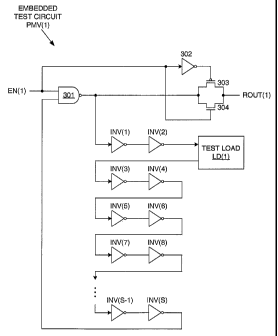
example, Fig. 3 shows an exemplary schematic diagram of embedded test circuit
PMV(1 ), according to an embodiment of the invention. Embedded test circuit
PMV(1 ) includes inverters INV(1 )-INV(S), a test load LD(1 ), a NAND gate
301,
an inverter 302, a PMOS transistor 303, and an NMOS transistor 304. Inverters
1o INV(1 )-INV(S) and test load LD(1 ) are serially connected between the
output and
a first input of NAND gate 301. Transistors 303 and 304 are configured as a
pass gate at the output of NAND gate 301. An enable signal EN(1 ) is provided
to a second input of NAND gate 301 and the gate of NMOS transistor 304.
Inverter 302 inverts enable signal EN(1 ) and provides the inverted output to
the
gate of PMOS transistor 303.
When enable signal EN(1 ) is asserted HIGH, the pass gate formed by
transistors 303 and 304 is turned on, and the output of NAND gate 301 is
provided as an output signal ROUT(1 ). Meanwhile, the logic HIGH enable signal
EN(1 ) at the second input of NAND gate 301 causes NAND gate 301 to operate
2o as an inverter with respect to the signal provided to its first input (from
inverter
INV(S)). When configured as an inverter in this manner, NAND gate 301 and
(the even number of) inverters INV(1 )-INV(S) form a ring oscillator. The
output
of the ring oscillator can then be read as output ROUT(1 ).
The frequency of output ROUT(1 ) is dependent on the delays generated
by inverters INV(1 )-INV(S) (and NAND gate 301 ) and test load LD(1 ). The
inverter delays are mainly related to the speed of the transistors making up
those
inverters, and therefore correspond to FEOL (Front End Of the Line) delays in
FPGA 210 (shown in Fig. 2). FEOL components are generally transistors, which
are formed directly in or on the semiconductor substrate during the early
stages
so of the manufacturing process. For example, the high-power input/output
(I/O)
transistors in IOBs 212 are one type of FEOL component. The high-speed core
transistors in CLBs 211 are another type of FEOL component. Various other
types of FEOL components will be readily apparent.
6
CA 02548312 2006-06-05
WO 2005/064355 PCT/US2004/041479
Transistor speed (i.e., the speed at which signals are transferred between
the data terminals of a transistor) is the main source of FEOL delay, and is
governed by transistor physical characteristics (e.g., gate length, gate oxide
thickness). For example, an I/O transistor, which has a relatively thick gate
oxide to provide robust handling of high power signals, will have a lower
transistor speed than a core transistor, which has a relatively thin gate
oxide and
is specifically designed for high speed operation.
To prevent performance differences between different types of transistors
from complicating the analysis, the ring oscillator in each embedded test
circuit
1o PMV(1 )-PMV(N) can be formed using a single type of transistor. For
example,
inverters INV(1 )-INV(S) and NAND gate 301 in embedded test structure PMV(1 )
shown in Fig. 3 could all be made up of I/O transistors (i.e., transistors
formed
during the same process steps and following the same design rules as the I/O
transistors in IOBs 212 of FPGA 210). A different embedded test structure
15 PMV(2) might include only high speed core transistors. In this manner, the
output of any particular embedded test circuit is related to a single type of
FEOL
component.
Meanwhile, test load LD(1 ) is either a direct short (i.e., a low-resistance,
physically short electrical connection) between the output of inverter INV(2)
and
2o the input of inverter INV(3), or else is an interconnect simulation
structure that is
formed in one of the metal or via layers of FPGA 210. When test load LD(1 ) is
a
direct short, embedded test circuit PMV(1 ) is classified as an "unloaded"
test
circuit, since no additional delay is added by test load LD(1 ). Thus, the
output
delay of the ring oscillator is driven solely by the ring oscillator itself.
However,
2s when test load LD(1 ) is an interconnect simulation structure, embedded
test
circuit PMV(1 ) is classified as a "loaded" test circuit, since test load LD(1
) adds a
substantial BEOL delay element into output signal ROUT(1 ), and so the ring
oscillator output delay is driven by both the ring oscillator structures
(inverters)
and test load LD(1 ).
3o BEOL (Back End Of the Line ) components mainly include the
interconnect structures formed during the latter stages of IC production. The
complex routing requirements of modern ICs can lead to long and densely
packed layers of metal wires that significantly affect the IC performance.
Test
load LD(1 ) can mimic this BEOL delay by incorporating a wire routing path
CA 02548312 2006-06-05
WO 2005/064355 PCT/US2004/041479
between the output of inverter INV(2) and the input of INV(3) that physically
resembles a typical or average interconnect path in FPGA 210.
BEOL components are defined by the particular process layer in which
they are formed. For example, the interconnects formed in the metal-1 layer
(M1
interconnects) represent a first type of BEOL component, while the
interconnects
formed in the metal-2 layer (M2 interconnects) represent a second type of BEOL
component. In a similar manner, the plugs (vertical interconnects) formed
through the via-1 layer between the M1 and M2 layers (V1 interconnects)
represent a third type of BEOL component. Thus, the total number of BEOL
1o component types will depend on the total number of interconnect layers used
to
produce a particular IC.
For example, many modern ICs, such as FPGAs, include nine metal
layers and eight via layers (i.e., seventeen total interconnect layers).
However,
components formed in upper metal layers generally include much thicker/wider
geometries than those formed in lower metal layers. Therefore, the signal
delay
contributions from interconnect layers are mainly determined by the lower
metal
layers of an IC (e.g., metal layers M1, M2, M3, and M4, and via layers V1, V2,
and V3). According to an embodiment of the invention, only these seven lower
of interconnect layers are included as BEOL components in the IC performance
2o characterization.
According to an embodiment of the invention, embedded test circuit
PMV(1 ) can include a test load LD(1 ) that corresponds to a single type of
BEOL
component - i.e., a test load LD(1 ) that provides a delay contribution that
is
mainly due to that single type of BEOL component. For example, to create a
correspondence to M1 interconnects, test load LD(1) could be formed in metal
layer M1. The more closely the configuration (i.e., the size, spacing,
orientation)
and layout of test load LD(1 ) in metal layer M1 matches the layout of actual
M1
interconnects, the more accurately test load LD(1 ) represents those M1
interconnects.
3o Note that some of this matching occurs simply due to the fact that the bulk
of test load LD(1 ) is formed in the appropriate interconnect layer (e.g.,
layer M1 ).
However, according to various embodiments of the invention, test load LD(1 )
can
include an interconnect layout that simulates an "average" M1 interconnect
layout (i.e., an interconnect layout that resembles a typical routing path
within
s
CA 02548312 2006-06-05
WO 2005/064355 PCT/US2004/041479
metal layer M1 ) or a "worst case" M1 interconnect layer (i.e., an
interconnect
layout that mimics the most problematic routing portions) within metal layer
M1).
Test load LD(1 ) can even include an exact duplicate of an M1 interconnect
path
from the functional portion of the IC.
Note that the output of each embedded test circuit PMV(1 )-PMV(N)
shown in Fig. 2 will include both FEOL and BEOL delay contributions,
regardless
of whether the test circuit is unloaded or loaded. For example, while the
output
delay from an unloaded test circuit will be primarily driven by the (FEOL)
transistors making up the ring oscillator, the (BEOL) interconnects that
connect
1o all those transistors will also have some effect. Meanwhile, a loaded test
circuit
will include the same FEOL delay effect from its ring oscillator transistor,
but will
also include a much larger (BEOL) interconnect delay effect due to the metal
or
via layer simulation structure in the test load.
Thus, while a rough idea of the relative delay contributions from FEOL
is and BEOL components can be determined by simply subtracting the output
delay of an unloaded test circuit from the output delay of a loaded test
circuit, a
more accurate determination of the FEOUBEOL delay contributions requires a
more sophisticated approach. Further complicating this determination of delay
contributions from specific FEOL or BEOL components (and relatedly, the
2o identification of specific variations in FEOL and/or BEOL parameter values)
is
the fact that a change in a BEOL parameter value will have different effects
on
the output delays of loaded and unloaded test circuits. These differing
effects
are illustrated in Figs. 4A and 4B.
Figs. 4A and 4B show sample graphs of test circuit outputs (output
25 delays) for embedded test circuits that include various different FEOL and
BEOL
components. Fig. 4A shows several graphs of embedded test circuit output
delay versus transistor speed ("transistor corner") for unloaded test circuits
having different types of transistors (I/O transistors and core transistors)
and for
loaded test circuits having test loads simulating different interconnect
layers
30 (metal-3 (M3), via-3 (V3), and metal-4 (M4)).
Output delay in Fig. 4A is graphed at three different transistor speeds: a
nominal, or target, speed "TT", a fast speed "FF" that is 20% faster than
nominal
speed TT, and a slow speed "SS" that is 25% slower than nominal speed TT.
Note that as transistor speed increases (from TT to FF), the output delay for
CA 02548312 2006-06-05
WO 2005/064355 PCT/US2004/041479
each embedded test circuit decreases to about 80% of the nominal output delay
value. Similarly, as transistor speed decreases (from TT to SS), the output
delay
for each embedded test circuit increases to about 125% of the nominal output
delay value.
Thus, the data in Fig. 4A indicates that transistor speed variations
produce roughly the same change in output delay for all embedded test circuits
that incorporate those transistors, regardless of whether those embedded test
circuits are loaded or unloaded. Note further that the change in output delay
essentially tracks the change in transistor speed (e.g., increase in
transistor
1 o speed of 20% results in roughly 20% decrease in delay), since transistor
speed
is generally directly proportional to propagation speed.
However, unlike FEOL parameter variations, changes in BEOL parameter
values will typically affect unloaded and loaded test circuits differently.
Fig. 4B
shows several graphs of embedded test circuit output delay versus interconnect
capacitance for unloaded test circuits (formed using I/O transistors or core
transistors) and for loaded test circuits (that include test loads simulating
different interconnect layers, such as metal-3 (M3), via-3 (V3), and metal-4
(M4)).
Output delay in Fig. 4B is graphed at three different interconnect
20 -capacitance values: a nominal, or target value NOM C, a low capacitance
value
LO_C that is 25% lower than the target value, and a high capacitance value
HI C that is 25% higher than the target value. The lower the capacitance of an
interconnect structure, the faster that signal propagation can take place
(i.e., the
less signals are delayed by the interconnect structure).
25 Accordingly, as interconnect capacitance decreases by 25%, the output
delays of the embedded test circuits all decrease. However, while the unloaded
test circuits (I/O and core transistors) exhibit a roughly 6% decrease in
output
delay (to 94% of the nominal delay), the loaded test circuits (M3, V3, and M4
interconnects) exhibit a roughly 20% decrease in output delay (to 80% of the
3o nominal delay). Similarly, as interconnect capacitance increases by 25%,
the
output delays of the embedded test circuits increase by roughly 6% for the
unloaded test circuits and by roughly 20% for the loaded test circuits.
Thus, as indicated by the graph of Fig. 4B, the effects of BEOL parameter
value variations have a small effect on unloaded test circuit output delay,
and a
to
CA 02548312 2006-06-05
WO 2005/064355 PCT/US2004/041479
much larger effect on loaded test circuit output delay. Therefore, to obtain a
more accurate representation of the performance-related effects of BEOL (and
FEOL) components requires that a set of model equations be created and
solved.
According to an embodiment of the invention, a model equation
corresponds to a particular embedded test circuit, and provides an expected
output delay based on delay contributions from both FEOL and BEOL
parameters (i.e., FEOL and BEOL characteristics such as transistor speed and
interconnect capacitance). The model equation therefore includes at least one
1o FEOL parameter variable modified by a FEOL correction factor and at least
one
BEOL parameter variable modified by a BEOL correction factor. The FEOL and
BEOL correction factors represent the effect of a change in the FEOL or BEOL
parameter variable, respectively, on the output of the model equation.
For example, a sample model equation for the output delay X;~ of an
15 unloaded test circuit can be given by the following:
X;~ _ (1 + CFF*~F;) * (1 + CBF*~B~) ~1)
where ~F; is the change in the value of a particular FEOL parameter F; (e.g.,
2o transistor speed), dB~ is the change in the value of a particular BEOL
parameter
B~ (e.g., interconnect capacitance for M1 interconnects), CFF is an FEOL
correction factor representing the effect of variations in FEOL parameter F;
on
the output delay of the unloaded test circuit, and CsF is a BEOL correction
factor
representing the effect of variations in BEOL parameter B~ on the output delay
of
25 the unloaded test circuit. Note that while normalized terms (i.e., terms
that
indicate a deviation from a nominal value, rather than an absolute value) are
used for exemplary purposes, the same principles can be applied to absolute
terms.
In a similar vein, a sample model equation for the output delay Y;~ of a
30 loaded test circuit can be given by the following:
Y;~ _ (1 + CFB*OF;) * (1 + CAB*AB~) L
where CFB is an FEOL correction factor representing the effect of variations
in
FEOL parameter F; on the output delay of the loaded test circuit, and CBB is a
11
CA 02548312 2006-06-05
WO 2005/064355 PCT/US2004/041479
BEOL correction factor representing the effect of in parameter Bj on the
output
delay of the loaded test circuit.
Note that while Equations 1 and 2 both based on a single FEOL
parameter (FEOL variable ~F;) and a single BEOL parameter (BEOL variable
~Bj) for exemplary purposes, according to various other embodiments of the
invention, a model equation can include terms related to any number of FEOL
and BEOL parameters. For example, Equation 1 described above could be
replaced with the following:
X~j = (1+CFF*0Fi)*(1-f-CgFj*0Bj)*(1-1-CgFk*~Bk)* ...
where aBj and ~B~ are the changes in the values of BEOL parameters Bj and Bk
(e.g., interconnect capacitance for M1 interconnects and interconnect
capacitance for V1 interconnects), respectively, CBFj is a BEOL correction
factor
representing the effect of variations in BEOL parameter Bj on the output delay
of
the unloaded test circuit, and CBF~ is a BEOL correction factor representing
the
effect of variations in BEOL parameter Bk on the output delay of the unloaded
test circuit.
Note also that according to an embodiment of the invention, each FEOL
or BEOL parameter can be associated with a set of FEOL or BEOL correction
factors, respectively. For example, the model equation associated with a core
transistor-based test circuit could include a different FEOL correction factor
for
each different type of BEOL parameter (e.g., CFF(1 ) for the effect of M1
capacitance in an unloaded core transistor test circuit, CFF(2) for the effect
of V1
capacitance in an unloaded core transistor test circuit, CFB(1) for the effect
of M1
capacitance in a loaded core transistor test circuit, CFB(2) for the effect of
V1
capacitance in a loaded core transistor test circuit, etc.). Similarly, the
model
equation associated with a M1 interconnect-loaded test circuit could include a
different BEOL correction factor for each different type of FEOL parameter
(e.g.,
3o CBF(1) for the effect of M1 capacitance on core transistors in an unloaded
test
circuit, CBF(2) for the effect of M1 capacitance on I/O transistors in an
unloaded
test circuit, CBB(1 ) for the effect of M1 capacitance on core transistors in
a loaded
test circuit, CBB(2) for the effect of M1 capacitance on I/O transistors in a
loaded
test circuit, etc.).
12
CA 02548312 2006-06-05
WO 2005/064355 PCT/US2004/041479
However, as indicated by the graph in Fig. 4A, variations in FEOL
parameter values tend to have a consistent effect on test circuit output,
regardless of the type of interconnect loading included in the test circuit.
Therefore, according to an embodiment of the invention, the set of model
equations for an IC can be simplified by using a single FEOL correction factor
(i.e., CFF = CFB). Since transistor speed has a roughly 1:1 relationship with
signal propagation delay, if the FEOL parameter is transistor speed, this
single
FEOL correction factor can be set equal to one (100%), as indicated below:
1 o CFF = CAB = 1 L4l
Likewise, as indicated by the graph in Fig. 4B, variations in BEOL
parameters tend to have a consistent effect on loaded test circuits and a
consistent effect on unloaded test circuits. Therefore, according to an
embodiment of the invention, instead of different BEOL correction factor for
every possible FEOL and BEOL parameter combination, the set of model
equations for an IC includes only two BEOL correction factors: a first BEOL
correction factor representing the effect of changes in a BEOL parameter on
the
output of an unloaded test circuit, and a second BEOL correction factor
2o representing the effect of changes in the BEOL parameter on the output of a
loaded test circuit.
For example, as indicated in the graph of Fig. 4B, increasing or
decreasing interconnect capacitance by 25% increases or decreases,
respectively, all unloaded test circuit (FEOL) output delays by roughly 6%,
and
increases or decreases, respectively, all loaded test circuit (BEOL) output
delays
by roughly 20%. Therefore, BEOL correction factor CBF (i.e., the effect of
BEOL
parameter variations on unloaded test circuit output) can be determined by
n~rmalizing the FEOL output delay by the change in capacitance, as shown
below:
CBF = 6%/25% = 24% (0.24)
13
CA 02548312 2006-06-05
WO 2005/064355 PCT/US2004/041479
Similarly, BEOL correction CBB (i.e., the effect of BEOL parameter
variations on loaded test circuit output) can be determined by normalizing the
BEOL output delay by the change in capacitance, as shown below:
CBB = 20%l25% = 80% (0.80)
These values of BEOL correction factors CBF and CBB can then be
substituted in to all unloaded and loaded model equations, respectively. For
example, substituting Equations 4 and 5 into Equation 1 yields:
X;~ _ (1 + aF;) * (1 + 0.24*OB~)
Similarly, substituting Equations 4 and 6 into Equation 2 yields:
Y;~ _ (1 + ~F;) * (1 + 0.80*OB~) ~8~
In this manner, model equations can be defined for all combinations of FEOL
and BEOL parameter variables.
Once the model equations have been defined (e.g., Equations 7 and 8),
2o they can be solved for the parameter variables, thereby generating a set of
parameter equations (i.e., an equation for a particular FEOL or BEOL
parameter)
that are all functions of output delays (e.g., X;~ and Y;j). The actual
(measured)
output delays can then be substituted into the parameter equations to generate
parameter values for the various FEOL and BEOL components, thereby allowing
2s any problematic deviations to be directly detected.
For example, model Equations 7 and 8 can be solved for parameter
variables OF; and OBE as follows. First, solving Equation 7 for OF; yields:
0F; = X;~/(1 + 0.24*~B~) - 1 L
Similarly, solving Equation 8 for ~F; yields:
~F; = Y;~/(1 + 0.80*~B~) - 1 [10]
14
CA 02548312 2006-06-05
WO 2005/064355 PCT/US2004/041479
Equation 9 can then be substituted into Equation 10 to yield:
O;~/(1+0.24*6B~) - 1 = Y;~/(1+0.80*AB~) - 1 [11]
which can then be solved for BEOL variable OBE as indicated below:
0B~ _ (Y;~ - X;i)~(0.80*X;~ - 0.24*Y;i) [12]
In this manner, a parameter equation for ~B~ as a function of output delays
X;~
1o and Y;~ can be derived. Equation 12 can then be substituted into Equation 9
to
generate a parameter equation for ~F; as a function of output delays X;~ and
Yg,
as indicated below:
x~~ _ 1 [13]
OFi -
0 . 2 4 (Y1~ - Xi~ )
1 +
0 . 8 0 * Xi~ - 0 . 2 4 * Yip
Measured values for output delays X;~ and Y;i from the appropriate unloaded
and
loaded embedded test circuits, respectively, can then be substituted in to
parameter equations 12 and 13 to provide values for BEOL parameter ~B~ and
FEOL parameter AF;, respectively. In this manner, the BEOL delay contributions
2o to the FEOL test circuit measurements can be eliminated, and vice versa.
Therefore, the source of any performance-affecting problems in an IC can be
quickly isolated down to the particular FEOL andlor BEOL parameter(s).
Figs. 5A-5B and Figs. 6A-6B are graphs of experimental data that indicate
the applicability of model Equations 12 and 13. Fig. 5A shows a graph of four
sets of experimental data, set 1 A, 1 B, 2A, and 2B. Data sets 1 A and 1 B
include
output delay measurements from a first group of unloaded (FEOL) test circuits,
while data sets 2A and 2B include output delay measurements from a second
group of unloaded test circuits. For testing purposes, the second group of
unloaded test circuits was designed and processed to have a higher metal-1
layer capacitance than the first group of unloaded test circuits. Thus, for
the
reasons described above, the output delay values associated with the second
is
CA 02548312 2006-06-05
WO 2005/064355 PCT/US2004/041479
group of unloaded test circuits (i.e., data sets 2A and 2B) are greater than
the
output delay values associated with the first group of unloaded test circuits
(i.e.,
data sets 1 A and 1 B).
Fig. 5B shows a graph of the experimental data from Fig. 5A, after the
metal-1 layer (BEOL) capacitance delay contributions have been removed from
the output delay measurements, using Equation 13. Data sets 1 A, 1 B, 2A, and
2B are converted in this manner into "FEOL-only" data sets 1 A', 1 B', 2A',
and
2B', respectively. The high degree of correlation between data sets 1 A', 1
B',
2A', and 2B' indicates that Equation 13 provides effective removal of the BEOL
1 o delay contributions. Note that the remaining variations among data sets 1
A', 1 B',
2A', and 2B' are due to transistor process variations.
Similarly, Fig. 6A shows a graph of four new sets of experimental data,
sets 3A, 3B, 4A, and 4B. Data sets 3A and 3B include output delay
measurements from a first group of loaded test circuits, while data sets 4A
and
4B include output delay measurements from a second group of loaded test
circuits. For testing purposes, the second group of loaded test circuits was
designed and processed to include transistors having higher threshold voltages
(Vtsat) than the transistors in the first group of loaded test circuits. Thus,
for the
reasons described above, the output delay values associated with the second
2o group of loaded test circuits (i.e., data sets 4A and 4B) are higher than
the output
delay values associated with the first group of loaded test circuits (i.e.,
data sets
3A and 3B).
Fig. 6B shows a graph of the experimental data from Fig. 6A, after the
transistor-related (FEOL) delay contributions have been removed from the
output
delay values, using Equation 12. Data sets 3A, 4A, 3B, and 4B are converted in
this manner to "BEOL-only" data sets 3A', 4A', 3B', and 4B', respectively. The
high degree of correlation between data sets 3A', 4A', 3B', and 4B' indicates
the
Equation 12 provides effective removal of the FEOL delay contributions. Note
that the remaining variations among data sets 3A', 4A', 3B', and 4B' are due
to
3o metal-1 process variations.
Fig. 7 shows a flow diagram of a performance analysis methodology in
accordance with an embodiment of the invention. In a "CREATE EMBEDDED
TEST CIRCUITS" step 710, a wafer is processed to include multiple embedded
test circuits in each IC, wherein each embedded test circuit includes a ring
16
CA 02548312 2006-06-05
WO 2005/064355 PCT/US2004/041479
oscillator and test load, as described above with respect to Fig. 3. Then, in
a
"MEASURE DELAYS" step 720, the output delays from each embedded test
circuit is measured. Note that according to various embodiments of the
invention, this testing can be performed before or after the wafer is diced
into
individual IC chips. Note that according to another embodiment of the
invention,
the ICs formed on the wafer can comprise programmable logic ICs (e.g., FPGAs)
that are configured into measurement circuits to read the output delays of the
embedded test circuits.
In a "DEFINE MODEL EQUATIONS" step 730, a model equation is
1o defined for each embedded test circuit in an IC, wherein each model
equation is
a function of at least one FEOL parameter and one BEOL parameter of the IC.
Then, in a "SOLVE MODEL EQUATIONS" step 740, the model equations are
solved for the FEOL and BEOL parameters to generate a set of parameter
equations that are functions of the output delays of the embedded test
circuits.
Note that according to various embodiments of the invention, steps 730 and 740
can be performed before, after, or concurrently with steps 710 and 720.
Finally, in a "GENERATE PARAMETER VALUES" step 750, the output
delays measured in step 720 are substituted into the parameter equations
created in step 740 to determine actual values for the FEOL and BEOL
2o parameters of interest. Any deviation from expected parameter values can be
indicative of a process or design problem that may provide performance
enhancement if corrected.
The various embodiments of the structures and methods of this invention
that are described above are illustrative only of the principles of this
invention
2s and are not intended to limit the scope of the invention to the particular
embodiments described. Thus, the invention is limited only by the following
claims and their equivalents.
17