Note: Descriptions are shown in the official language in which they were submitted.
CA 02548501 2008-12-19
METHOD FOR OBTAINING NANOPARTICLES
RELATED APPLICATIONS
This application claims priority to RU patent #2242532 published on December
20, 2004.
FIELD OF THE INVENTION
The invention is intended for obtaining nanosize particles that find
application
in various fields of science and technology; in particular, metallic
nanostructures are
regarded as a promising material for development of new sensors and electronic
and
optoelectronic devices and for design of new types of highly selective solid-
state
catalysts.
BACKGROUND OF THE INVENTION
As shown in a number of recent publications. nanostructures with a surface
particle density on the order of 1012 cm Z are promising for development of
efficient
nanoelectronic devices, such as ultrafast switches or subminiature memory
cells ((K.H.
Yoo, J.W. Park, J. Kim, K.S. Park, J.I. Lee and J.B. Choi. Appl. Phys. Lett.,
1999,
v. 74 (14). p. 2073)).
For example, in the case of densely packed nanostructures with grain size of
-4 nm, it is possible to create storage devices with recording density of -
10" bit/cmZ
(F. Pikus and K. Likharev. Appl. Phys. Lett., 1997, v. 71, p. 3661; Y. Naveh
and K.
Likharev, Superlattices and Microstructures 2000, v. 27, p.1). In the limiting
case of
grain size diminished to -1 nm, the recording density increases to 1012
bit/em2.
SUMMARY OF THE INVENTION
In the last decade, a new area of catalytic chemistry has formed and is
rapidly
developing now: heterogeneous catalysis on nanostructured materials (P.S.
Vorontsov, E.I. Grigor'ev, S.A. Zav'yalov, L.M. Zav'ynlova, T.N.
Rostovschikova,
O.V. Zagorskaya, Himicheskaya Physica 2002, v. 21, p.1). Most of the catalysts
that
are studied in laboratories and used in technological practice contain
nanoparticles,
i.e., particles with dimensions in the range 1-100 nm. The fundamental
distinction
-1-
CA 02548501 2008-12-19
between nanoparticles and bulk materials is that the fraction of surface atoms
in
nanoparticles is comparable with that in the bulk and the radius of curvature
of the
surface is comparable with the lattice constant. It is a commonly accepted
opinion that
it is these specific features that ensure the high catalytic activity of
nanostructured
catalysts as compared with their analogues based on bulk materials. The most
promising for quite a number of practically important applications are
catalysts based
on metallic nanostructures, which contain nanoparticles of Cu, Pt, Pd, Ni, Fe,
Co, and
other metals.
The known methods for obtaining nanoparticles of various materials can be
divided into two large groups: in the first of these, nanoparticles are formed
by
combination of atoms (or more complex radicals and molecules), and in the
second,
by dispersion of bulk materials.
Numerous methods based on combination of atoms (radicals, molecules) into
nanoparticles are known, including, e.g., thermal evaporation and condensation
(see
S.Tohno, M.Itoh, S.Aono, H. Takano, J. Colloid lnterface Sci., 1996, v.180,
p.574),
ion sputtering (see US Patent No. 5,897,827, Int. Cl. H 01 M 04/36, published
09.03.1999), reduction from solutions (see US Patent No. 6,090,858; Int. Cl. C
09 K
03/00, published 18.07.2000), and reduction in microemulsions (see H.Herrig,
R.Hempelmann, Mater. Lett. 1996. v.27, p.287).
For example, in the method for obtaining nanoparticles by reduction of metals
from solutions, an aqueous solution of a metal salt and an anion-active
compound
with COO-, S042-, or S03Z- groups as a reducing agent is heated to 50-140 C,
with the
result that the metal salt is reduced to give metallic nanoparticles (see US
Patent No. 6,572,673,
Int. Cl. B 22 F 9/24, published June 3, 2003).
In the known method for deposition of submonolayer and monolayer coatings
composed of gold and silver nanoparticles, the structure is formed via capture
of
metallic nanoparticles prepared in a colloid solution onto the support surface
covered
by a special organic film (see US Patent No. 6,090,858; Int. CI. C 09 K 03/00,
published 18.07.2000).
The advantage of this method consists in that it enables immobilization on the
support surface of spherical nanoparticles with average size in the range from
3 to 100
nm (depending on preparation conditions) with rather narrow size dispersion.
However, the maximum surface density of particles on the support surface does
not
exceed in this case 0.5 dZ (where d is the average size of nanoparticles).
Accordingly,
-2-
CA 02548501 2006-03-08
WO 2005/023460 PCT/IB2004/051445
exchange of electrons between neighboring particles is hardly probable and it
is
irnpossible to use structures of this kind to create catalysts operating in
the maximum
efficiency mode and to design eflicient nanoelectrcrnic devices in wltich the
effects of
interaction and charging of densely packed particles are intportant.
A method is known for obtaining silicon clusters in structural voids ol'
zeolites, which consists in introduction of disilane (Si2H(,) into these voids
and its
subscquent oxidation. Silicon liberated in the reaction assembles into
nanoclusters.
'I'his technique is a particular case of -he cheniical vapor deposition (CVD)
method
(see Dad 0., Kuperman A., MacDonald P.M., Ozin G.A. - A New Forni of
Lutninescent Silicon - Synthesis of Silicon Nanoclusters in Zeolite-Y. -
Zeolites and
Related Microporous Materials: State of the Art., 1994. v.84, p.p. 1107-1114).
T'he
method cannot be used to form silicon nanostructures in local regions because
it
transforms the zeolite substrate across virtually its whole thickness. An, in
fact,
homogeneous composite material is produced by this known technique.
Also known is a method of cryochemical synthesis of nietal-polymer
nanostructures (see LJ. 'l-rakhtenbers et al., Zh. Fiz. Khim.. 2000, vol. 74,
p. 952).
"f'he main advantage o1" nietal-polymer nanostructures is their rather high
specific activity as catalysts. However, as the content of metal increases,
the catalytic
activity of catalysts of this kind decreases because crysialline nanoparticles
tornied by
this technique coagulate when coming irr contact with one another. Moreover,
the
fiindamental aspects of nanoparticle growth, iuhcrent iri the cryochcniicai
synthesis,
necessarily lead to a broad distribution of particle sizes and shapes.
'1"o methods of the second group (forrnation of nanoparticles by dispersion of
materials) should be referred the technique (see K. Deppert and L. Samuelson.
Appl.
Phys. Len.- 1996, v.68(10), p.1409) in which the initial flow of polydisperse
liquid
drops is produced in the course of thermal evaporation of an overheated
material.
capture of drops by ttie flow of an inert carrier gas (nitrogen), and,
further, successive
separation of particles via interaction of' charged particles in the gas flow
with the
electric field in the differential mobility analyzer_ The thus formed flux of
charged
nanoparticles is deposited onto the substrate. 7"his method, named "Acro taxi"
by its
authors, makes it possible to obtain a monodisperse flux of'charged nanosize
particles
of metals (and semiconductors). The method yields 26-30-nm crystalline
particles,
with the particle size dispersion not less than 50% (the size scatter directly
depends on
the number of separation stages). Among disadvantages of the method are its
low
-3-
CA 02548501 2006-03-08
WO 2005/023460 PCT/IB2004/051445
output capacity and relatively wide particle size dispersion. Moreover, the
method
gives no wav of forming metallic particles with high density of particle
packing,
because, as the density increases, crystalline nanoparticles coagulate into
more bulky
formations.
The method for obtaining nanoparticles, which is the closest to that cla.inied
in
this patent application and is chosen as the prototvpe, was described in
(V.M.Kozhevin, D.AYavsin. V.M.Kouznetsov, V.M.Busov, V.M.Mikushkin, S.Yu.
Nikonov, S.A.Gurevich, and A.Kalobov, J.Yac. Sci. "J'echn. B, 2000, v.18,
no.3,
p.1402). This method is based on ablation of a metallic target under the
action of light
generated by a liigh-power pulse-periodic laser. Rather severe modes of target
irradiation are chosen, in which, together with evaporation of the target, a
great
number of micrometer- and submicrotneter-size drops of' molten metal are
ejected
from its surface. Optical breakdown of a vapor near the target surface leads
to the
formation of a hot laser torch plasnia. while the temperature and density of
this
plasma are determined by the type of a tnetal and conditions of' target
irradiation
(power density of the incident laser light, angle of ittcidence, etc.). In the
laser torch
plastna, liquid metal drops ejected from the target surf'ace are charged to a
critical
value, to the threshold of capillary instabitity, on reaching which drops
start to break
down to produce a tnultitude of finer (daughter) drops. 'I'he daughter drops
are
charged to above the instability threshold, so that the breakdown process that
has
started is of a cascade nature. I lowever. it was shown in the publication
mentioned
above that the process of drop breakdown continues only to a certain extent.
This
process terminates because, as the size of charged drops steadily decreases,
the
current of autoelectronic emission from their surface grows, which, in the
end, leads
to a decrease in the drop charge to below the instability threshold. For most
of metals,
the size of drops formed by the end of the breakdown process is on the order
of'
several nanometers. 'Ifie abrupt ternlination of the process ensures a
sutliciently
narrow size distribution of the resulting nanopatticles. Thus, the breakdown
of liquid
micrometer- and submicrometer-size meta4 drops in the laser torch plastna
yields a
great number of nanometer-size particles with a narrow size distribution.
I'he prototype method described has been used to deposit onfo the substrate
surfaee single-layer coatings composed of 8-10 nni copper nanoparticles. Even
though
the particle size dispersion was not evaluated for the prototype method, it
may be
-4-
CA 02548501 2006-03-08
WO 2005/023460 PCT/IB2004/051445
concluded, on the basis of'the results obtained in this study . that the size
distribution
is tnuch narrower than. e.g., that for the "Aero taxi" method.
However, the conditions ttiat could ensure stable formation of nanoparticles
with amorphous structure have not been determined for the prototvpe method.
This
circumstance markedly restricts the possibility ot' reproducible formation of
nanostructures with high surface density of particles on the support surface,
which is
very itnportant. e.g., for carrying out effective catalysis and developing a
number of
nanoelectronic devices. This also hinders the industrial application of the
prototype
method.
It should also be noted that, as established by the authors, the range of
plasma
parameters in which an effective breakdown of liquid charged drops can be
achieved
is considerably wider. This makes it possible to produce nanoparticles not
only in a
laser-induced plasma, but also in a plasma #bt7ned by other, more
technalogically
conveniettt methods yielding a quasi-stationary plasma.
In the known niethod for obtaitiing nanoparticles, the conditions are close to
equilibrium, which leads to the format:ion of metallic particles that are, as
a rule, in tttc
crystalline state. The coalescence of crystalline nanoparticles gives rise to
severe
difficuities in formation of structures with a high density of particle
packing.
T'he aim of the claimed invention is to modify the known prototype tnethod by
developing such a procedure for obtaining nanoparticles that could be used to
deposit
onto the surface of a support nanopanicles with a narrow size dispersion and
amorphous structure, which makes it possible to achieve an esceedingly high
density
of nanoparticle packing. The improvement of the known prototype method also
includes raising the efficiency of conversion of the starting material into
nanoparticies.
The forrnulated problem can be solved by using the following procedure to
obtain nanoparticles. This procedure includes dispersion of a molten
tnaterial, supply
of the resulting liquid drops of this niaterial into a plasma formed in an
inert gas at a
pressure of I04-10'1 Pa, cooling of liquid nanoparticles formed in the said
plasma to
their solidification, and deposition of the resulting solid nanopariicies onto
a stipport,
with the plasma parameters satisfying the following relations
YR, R Rn+R
T, >1.4 = 10 ---- ..-......_........~ (1)
Rõ -i- 2 R
-5-
CA 02548501 2008-12-19
> 9a,-,' i + -" ~ (2)
~ +l~ >10""'7~ (3)
rp L
where R and r are, respectively, the maximum and minimum radii of the drops
fed
into the plasma, m;
Kj, - 7.5 = I f7' is tlte Debyc screening #engih, m;
Te is the electron temperature of the plasma, eV;
ne is the density of the plasma, m;;
id is the time of transit of the drops across the plasma, s;
Tp is the lifetime of the plasma, s;
Tm is the melting point of the material, K;
L is the characteristic distance along which the plasma pressure decreases by
a factor of e, m.
As a material that can be used to obtain nanoparticles can serve a metal, a
semiconductor, or a metal oxide.
The nanoparticles obtaincd can be deposited onto a support in an electric
field
whose strength vector makes a certain angle with the direction of nanoparticlc
motion,
c.g., in a nonunifonn clectric field.
The molten material can be dispersed, and the resulting drops fed into
the said plasma, by laser ablation of a target made of the said material in
the
atmosphere of an inert gas with a pressure of 10-4 - 10-2 Pa under the action
of light
generated by a pulsed-periodic YAG:Nd;+ laser operating at a wavelength of
1.06 gm
at a pulse length of no less than 20 ns, pulse leading front of less than 5
ns, and pulse
repetition frequency of no less than 10Hz. The power density of laser light
incident
on the target should be not less than 109 W/emZ.
The moltcn material can also be dispersed by applying to a pointed cathode
with tip radius not exceeding 10 m, made of a conducting material, an
electric field
with strength at the cathode tip apex of no less than 10' V/cm. The resulting
drops can be fed into a plasma formed in an electric discharge with pulse
duration of
-6-
CA 02548501 2006-03-08
WO 2005/023460 PCT/IB2004/051445
no less than 10 s, created in an inert gas at a. pressure of 10---10-1 Pa
between
electrodes at a potential difference of no less than 2 kV and simultaneous
action c+f a
magnetic field with a strength of' no less than 600 G, directed
perpendicularly to the
said electric field creating the said plasma.
The essence of the invention consists in that, in contrast to the known
prototype method, the parameters of the plasma used are chosen to meet the
requirement that conditions (1)-(3) should be satisfied simult:aneously.
'I'hese
conditions ensure a cascade fission of all the initial liquid drops of the
tnaterial,
injected into the plasma, and a fast cooling of the fonning liquid nanometer-
size drops
(final products of drop fission), such that the solid natnoparticles deposited
onto the
substrate have an amorphous structure. If these conditions are satisfied,
monodispersive structures cornposed of amorphous nanoparticles with variable
(including an exceedingly high) packing density can bc reproducibly formed,
wilh an
efficient conversion of the starting material into nanoparticles.
When practicing the claimed method, the density and electron teinperature of
plasma are chosen on the basis of the condition (1). In deriving this
condition, which
assumes that the initial drops are charged to Rayleigh's capillary instability
threshold
(A.I. Grigor'ev, S.O. Shiryaeva, Journal of 7'echnicat Phy.sics, 1991, v. 61
(3), p.
258), the charge of drops was calculated using the known dependence of the
floating
potential of the drops on plasma parameters (Yu.P. Raizer, Physics ot' Gas
i7ischarge,
Moscow: Nauka, 1987). It is noteworthy that the capillary instability
threshold was
formulated in the prototype method only for a drop with a certain radius R.
However,
the initial liquid drops injected into the plasma are actually always
characterized by a
certain size distribution, in which the inaxirnuin (R) and ntinimum (() drop
sizes can
be distinguished. For all the initial drops with sizes in the range from R to
r to be
charged to the instability threshold and to be involved in the process of
cascade
tission, the parameters of the plasma should be chosen with account ot'
condition ( I).
When this condition is not satisfied, only part of the initial drops will
undergo
division to a nanometcr size and, thereby, the etlieiency of nanoparticle
formation
will be markedly impaired.
It is also important that espression (1) is valid only in the case when the
initial
liquid drops remain in the plasma. for a sufficiently long time, during which
ttteir
stationary charge state is attained. The stationary state is attained if
condition (2),
which means that the time of drops transit across the volume occupied by the
plasma
-7-
CA 02548501 2006-03-08
WO 2005/023460 PCT/IB2004/051445
excceds the time in vvhich they are chargt-~d to the floating potential, is
satisfied. If this
is not the case, the initial drops will have not enough time to be charged
during their
residence in the plasma and their division will not occur. Thus, the fact that
condition
(I) is supplemented with condition (2) is a significant difTerence from the
prototype
method, which ensures that all the initial drops of the material, fed into the
plasma
zone, are involved in the fission process.
For the nanoparticles to be forined in the amorphous state, it is necessary to
ensure their cooling at the instant of hardening at a rate of no less than 10'
K/s.
Calculation of the rate of nanoparticle cooling via radiation loss shows that
the
required cooling rate is obtained at a particle size of less than 10 nm.
Accordingly, the
{5 condition ot' a fast cooling of nanopartictes is satisfied when the
radiation loss is not
cotnpensated for by the inflow of energy from ttre plasina. 'I'here are two
ways to mect
this rcquirement. In the first case of a nonstationary plasina, it is
riecessary that, after
the process of drop fission is complete, the plasma should rapidly expand and
cool
down. with the time of its cooling being shorter than the time of cooling of
nanopartic(es to the melting point. In the second case of a quasi-stationary
plasnia, it
is necessary that nanoparticles fermed in drops fission process should pass
the plasma
boundary region, where the pressure of the plasma decreases io the pressure of
the
inert gas, sufficiently rapidly. i.e., in a time shorter than the time
necessary for cooling
of nanoparticles to the melting point. The condition under which these
requirements
are satisfied is given by expression (3).
BRIEF DESCRIPTION OF THE DRAWINGS
'I'he claimed method for obtaining nartaparticles is illustrated by the
drawings
in which:
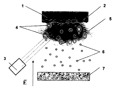
Figure I shows scheinatically how nanoparticles can be obtained by nieans of
laser dispersion (E is the electric field strength vector);
Figure 2 sliows a TEM 'stnage of a structt+re constituted by a substrate and
copper nanoparticles deposited on it;
Figure 3 shows a TEM image of a structure constituted by a substrate and
nickel nanoparticles deposited on it;
Figure 4 shows schematically the installation for plasma-assisted
electrodispersion, in which the claimed method for obtaining nanoparticles is
realized.
-8-
CA 02548501 2006-03-08
WO 2005/023460 PCT/IB2004/051445
DETA[LEll DESCRIPTION OF THE INVENTION
The schematic of the process tbr obtaining nanopartictes by laser dispersion
(Fig. 1). used in practicing the clairned method, includes a target I. whose
molten
surface layer 2 is dispersed under the action of a putsed-periodic laser 3 to
give liquid
drops 4, which, when passing the plasma zone 5, undergo division to
nanoparticles 6.
The resulting nanoparticles 6 are deposited onto a substrate 7. The process is
performed in an attnosphere of argon at a pressure of 10"4-10'2 Pa.
The installation for plasma-assisted electrodispersion, in which a stationary
plasma is formed, includes (see Fig..4) a vacuum chamber 8 in which a pointed
cathode 9, an anode with an aperture 11. a cathode 12 with an opening 13, and
an
annular anode 14 on which substrates 7 are mounted. The chamber is filled with
an
incrt gas at a pressure of 10"3-l0'1 Pa. Wtten an appropriate potential
ditlerence is
created betwecn the pointed cathode 9 and anode 10, molten drops 4 emerge
frorn the
surface of the cathode 9. When these drops pass the plasma zone 5, they are
divided to
form nanoparticies 6 and coarser (than the nanoparticles) drops 15.
T'he claimed niethod for obtaining nanoparticles is practiced as follows. A
molten material, from which nanoparticies are to be produced, is dispersed by
any
known tnethod (e.g., by atomization with a nozzle). The resulting liquid drops
are fed
into a plasnia tiarmed in an inert ilas at a pressure of 10'-10"1 I'a. As
inert gas can
serve any known inert gas. The liquid nanopartictes f(irmed in the plasma zone
are
cooled in the inert gas to hardening and then the resulting solid
na.noparticles are
deposited onto a support made of any solid material. As established by the
authors,
the plasma parameters should satisfy the relations:
s Rn R Ra, ~' R) 7 tta~ (1)
R,, -w2R
R ~
n;`' > 9r-' 1 + -" ; (2)
I { 10' > 10-s7 ; (3)
rp G
-9-
CA 02548501 2006-03-08
WO 2005/023460 PCT/IB2004/051445
where 12 and r are, respectively, the tnaxirnum and minimum radii of liquid
drops fed
into the plasma, m;
Ri) = 7.5 = 103 y~ /-e is the Debye screening length, m;
n,,
T, is the electron temperature of the plasma, eV;
nõ is the density of the plasma, m'3;
Td is the time of transit of liquid drops across the plasma zone, s;
rP is the lifetime of plasma, s;
T,r is the melting point of the conducting ntaterial, K;
L is the characteristic distance along which the plasma pressure decreases by
a factor
ofe, m.
As a niaterial that can be used to obtain nanoparticles cati serve both a
metal
and a semiconductor or a metal oxide.
It is advisable to deposit the nanoparticles obtained onto a support in an
electric field whose strength vector niakes a certain angle with the direction
of
nanoparticle motion, e.g., in a nonuniform electric field,
Example I. The claimed method for obtaining nanoparticies was practiced on
the basis of laser dispersion of such nietals as copper atid nickel (see Fig.
1). ln this
case, irradiation of the surface of the inetallie target I with a pulsed-
periodic laser 3
leads to melting of the surface layer 2 of the target I and the material of
the targel 1
evaporates. As a result of an optical breakdown of the vapor formed, a plasma
zone 5
with a thickness L? 100 m is formed near the surface of the molten layer 2 of
the
target 1. Under the action of plastna 5, the molten surface layer 2 beconies
unstable,
which leads to dispersion of the metal to give liquid particles 4 from the
nietal of the
target I. with the maximum and minimum radii of these particles being R= I m
and
r= 100 nni, respectively. Liquid drops 4 1'orined as a result of dispersion
are fed into
the plasma zone 5, which is heated by absorbed laser light. In the plasma zone
5,
drops 4 are chargcd to the floatirig potential, so that their charge is mainly
determined
by the temperature of electrons in plasma 5. If the amount of charge is such
that
Coulomb repulsion forecs exceed the surface tension force, then the drop 4
becomes
unstable (capillary instability) and st:arts to break down into smaller drops
6.
-10-
CA 02548501 2006-03-08
WO 2005/023460 PCT/IB2004/051445
The capillary instability develops if condition (I) is satisfied. This
condition
relates the electron ternperature (Te), the density of electrons in the plasma
(n,;), and
the maximum radius of particles 4 fed into the plasma zone 5(R). In order f'or
dispersed particles 4 to have enough time to obtain a charge sut'ticient for
their
transition to an unstable state, condition (2) should be satisfied. 'fhese
conditions
impose restrictions on the minimum electron temperature and density of plasma
5. For
particles 4 with sizes R = I -n and r = 100 nm, the required tetnperature of
electrons
is -30 eV, and the density of plasma 5, nc = 1018 cm-3. The necessary
parameters can
be obtained if the power density ot' laser light incident on the target
exceeds 10y
W/cmZ and the laser pulse has such a shape that the pulse-rise tinie is less
than 5 ns
and the full puise width exceeds 20 ns.
If conditions (1) and (2) are satisfied, this ensures that all liquid drops 4
fed
into the plasma zone 5 undergo division: the process occurs in the forin ol' a
caseade
with successive formation of increasingly tine drops and culminates in the
fortnation
ol' a great number of nanosize liquid drops 6. Depending on the ratio between
the
plasma expantion velocity of 6 and the motion velocit:y of nanoparticles 6,
liquid
nanoparticles 6 can either leave the region of hot plasma 5 and eventually
undergo
cooling and hardening, or cool down and harden because of the expansion of the
plasma cloud. For nanoparticles to have an amorphous structure in the solid
state, it is
necessarv to ensure a sufficiently high (-10' K/s) rate of'their cooling in
hardening.
Such a cooling rate is ensured by radiation loss if nanoparticles 6 are
outside the
plasma zone 5 at the instant of hardening. 's.e., if inequality (3) is
satisfied. lJnder the
conditions of the experiment described, the plasma lifetime rp = 1 lis, I_?
100 }im. If
copper or nickel is chosen as the inaterial of' the target 1, tlte motion
velocity of
nanoparticles 6, v,t = 3 104 am/s. and the melting point falls within the
range T,,,
=1350-1730 K. In this case, condition (3) is satisfied.
With the above-described paraineters of the process, copper and nickel
nanoparticles 6 were obtained (Figs. 2 and 3). Both copper and nickel
nanoparticles 6
were in the amorphous state.
l'articles 6 were deposited onto oxidized silicon substrates 7. 7'he size of
the
particles 6 was 5 nni for copper and 2.5 nm for nickel. The relative variance
of the
sizes of nanoparticles 6, evaluated using TEM images, did not exceed 20%. In
contrast to nanoparticles obtained using the prototype method, in which
nanoparticles
-Il-
CA 02548501 2008-12-19
are crystalline and coagulate when coming in contact with one another, the
size of the
nanoparticles 6 produced by the claimed method was found to be twice smaller.
This
is due to the choice of the rise time of the laser light pulse, which ensures
that
condition (2) is satisfied.
Example 2. The claimed method was practiced on the basis of an installation
for plasma-assisted electrodispersion, which is shown schematically in Fig. 4.
Molten
metal was dispersed by applying to a metallic pointed cathode 9 with a radius
of tip
curvature not exceeding 10 gm an electric field with a strength at the tip
apex of no
less than 10' V/s.
Molten drops 4 obtained at the tip 9 are delivered to the plasma zone 5
created
by a stationary or quasi-stationary discharge in an inert gas at a pressure of
10-3 - 10-1
Pa, to be charged there. The electron density in stationary discharges at
these
pressures is on the order of ne = 1010- 10ll cm 3 and, in accordance with
condition (1),
the required temperature of electrons should exceed 500 eV. To create such a
temperature, the potential difference between anode 9 and cathode 10 was set
to no
less than 2 W.
For drops 4 not to have enough time to be charged to the floating potential,
i.e., for condition (2) to be satisfied at a given electron density, the anode
9 and the
cathode 10 are to be mounted at a certain distance from each other, in
accordance with
the chosen inert gas pressure (about 5 cm).
If the above conditions are satisfied, drops 4 flying into the plasma zone 5
become unstable, which leads to the onset of their cascade fission.
The lifetime of stationary or quasi-stationary plasma 5 is long, and, in
contrast
to the case of laser dispersion, whether or not the inequality that describes
condition
(3) is satisfied is determined by the choice of parameter L. In the given
case, the value
of this parameter is close to the size of the opening in the cathode 10 and,
in view of
the requirements imposed by condition (3), it should not exceed 1 em.
Further, the forming nanosize drops 6 were separated from coarser drops 15
by choosing the dimensions of the annular anode 14, on which substrates 7 are
mounted. The potential difference between the anode 14 and the cathode 12 was
chosen in such a way that nanosize particles 6 were directed by the electric
field to the
substrate 7, and the trajectories of coarse particles 15 were not distorted.
The resulting
nanoparticles 6 were also in the amorphous state.
-12-
CA 02548501 2006-03-08
WO 2005/023460 PCT/IB2004/051445
't'hus, the claimed inethod yields nanosize spherical aniorphous particles
with a
narrow size dispersion.
-13-