Note: Descriptions are shown in the official language in which they were submitted.
CA 02548651 2006-06-07
WO 2005/063464 PCT/BE2005/000001
"Method of forminu a three-dimensional microstructure on a surface,
uses thereof, and microstructured products so obtained"
The present invention relates to a method of forming a three-
dimensional microstructure on a flat surface of a support, to the uses of said
s method, as well as to the products and in particular to the self-adhesive
films
comprising such a three-dimensionally microstructured surface.
I't is known to provide films made of adhesive which are sensitive to
pressure, and whose topography is conferred by contacting the three
dimensionally microstructured surface of a peelable protecting coating as
to support, which is essentially the inverse of the three-dimensional
microstructure with which the surface of adhesive is contacted, and methods
for the formation of such self-adhesive films. According to these methods, the
three-dimensional structures are obtained either by mechanically embossing
the support comprising a flat film made of silicone or by coating silicone on
a
is support which already presents a microstructured surface, in that case
matching the topography of the support. Although the methods for the
formation of such self-adhesive films generally turn out to be rather
satisfactory, they have limited application, as they can only be produced on
expensive polyethylene or polypropylene supports. In the case of polyethylene
2o and silicone supports, the formation of microstructures in the silicone is
carried
out by hot embossing at speeds on the order of 0.9 mlmin of the engraved
cylinder which is used for this purpose, which considerably slows the
productivity and raises the production costs of the finished products.
Various articles and other pressure sensitive microstructured adhesive
2s materials or films are disclosed by patent publications e.g. EP 149135
CA 02548651 2006-06-07
WO 2005/063464 PCT/BE2005/000001
-2-
discloses pressure sensitive adhesive structures having islands of adhesive,
EP 180598 discloses removable label stock having adhesive segments, and
EP 861307 discloses an adhesive sheet having a plurality of adhesive pegs
and also it should be mentioned patent application WO 97/43319 relating to
s top coat film useable in preparing a stable polymeric laminated data
carrying
device, said topcoat film comprising a topcoat layer being formed from a
composition comprising a polymerizable composition and a polymeric binder,
which is substantially plasticizer free, and wherein the ratio by weight of
polymerizable composition to polymeric binder is between 0.75:1 and 1.50:1
to inclusive. US patent 4,986,496 relates to an article capable of reducing
the
resistance to drag of a fluid flowing thereover, which comprises a thermoset
polymeric sheet formed in situ from the reaction product of an isocyanate with
a poiyol, said sheet having a surface contacting said fluid comprising a
series
of parallel peaks separated from one another by a series of parallel valleys.
is Patent application EP 0 382 420 A2 provides a composite plastic article
comprising a tough, flexible substrate, one face of which bears a .
microstructure of discontinuities, which microstructure has a depth of
0.025 mm to about 0.5 mm, and comprises a cured oligomeric resin having
hard segments and soft segments, the cured resin being substantially
2o confined to the microstructure portion of the composite.
One of the purposes of the present invention, consequently, consists in
overcoming the above-mentioned drawbacks and in providing a method of
forming a three-dimensional microstructure on a flat surface of a support
which wholly differs from the known processes consisting in deforming a
2s previous plane surface, presiliconized or not to get the desired final
microstructured surface.
For this purpose, according to the present invention, the above-
mentioned method of making a three-dimensional microstructure comprises
the application of a first flat and uniform layer of silicone on said surface
of
CA 02548651 2006-06-07
WO 2005/063464 PCT/BE2005/000001
-3-
support and the application on the first layer of silicone of a second three
dimensionally microstructured layer of silicone, said first layer and second
layer of silicone became integrally connected to thus form a common three-
dimensional microstructure ensuring anti-adhesive properties distributed
s regularly on the surface of the 'support, so that any flexible surface of
substrate, in particular a surface of adhesive deposited on said layers of
silicone will be microstructured by inverse replication of the three-
dimensional
microstructure formed by the two layers of silicone, said layers of silicone
being fixed by hardening by heating or by exposure to an ultraviolet or
to electronic radiation, or a combination thereof.
Another purpose of the present invention consists in providing a
method for three-dimensional microstructuring of a surface made of a flexible
substrate, in particular a surface of adhesive, which can be produced on any
type of substrate, such as papers, plastic films or others, and which allows
is one to work at very high speed, thus increasing the productivity
considerably
compared to the known prior methods.
For this purpose, according to the present invention, the above-
mentioned three-dimensional microstructuring method comprises the
application of a first layer of silicone, which is substantially flat and
uniform, on
2o a surface of a support, the application on the first layer of silicone of a
second
three dimensionally microstructured layer of silicone, where said first and
second layers of silicone become integrally connected thus forming a common
three-dimensional microstructure ensuring anti-adhesive properties which are
distributed evenly over the surface of the support, and the deposition of the
as flexible surface of substrate, in particular of the surface of adhesive, on
the
above-mentioned layers of silicone in such a manner that said surface made
of flexible substrate, in particular of adhesive, is microstructured by
inverse
replication of the common three-dimensional microstructure formed by the first
layer of silicone and the second layer of silicone, where said layers of
silicone
CA 02548651 2006-06-07
WO 2005/063464 PCT/BE2005/000001
-4-
are fixed by hardening by heating or by exposure to an ultraviolet or
electronic
radiation, or a combination thereof.
Advantageously, the first Payer of silicone comprises at least one
functionalized polyorganosiloxane with groups
_~ ; ~.h,..
'1
as crosslinking agent, and at least one functionalized polyorganosiloxane
which can react with the crosslinking agent, or it comprises a functionalized
polyorganosiioxanes with groups
-~-
to
as crosslinking agent, and at least one functionafized polyorganosiloxane with
groups
C
which can react with the crosslinking agent, where R comprises at feast one
is ethylenic unsaturation, and optionally, in one or the other case, an
activation
catalyst for the above-mentioned crosslinking reaction, and it is hardened by
heating or by exposure to ultraviolet or electronic radiation.
According to an advantageous embodiment of the invention, the above-
mentioned second layer of silicone comprises at least a polyorganosiloxane
zo and, advantageously, a polydimethylsiloxane with acrylate andlor epoxy
function, and optionally an activation catalyst.
CA 02548651 2006-06-07
WO 2005/063464 PCT/BE2005/000001
-5-
According to another advantageous embodiment of the invention, the
second. layer of silicone comprises a polydimethylsiloxane with acrylate
function and a catalyst of the ketone type, advantageously of the
benzophenone type, or it comprises a polydimethylsiloxane with epoxy
s function and a catalyst of the iodonium salt type, and it is hardened by
exposure to ultraviolet radiation.
According to yet another advantageous embodiment, the second layer
of silicone comprises no activation catalyst and it is hardened by exposure to
electronic radiation.
to The invention also concerns the three dimensionally microstructured
films, and the self adhesive films which comprise a surface such as one which
has been three dimensionally microstructured by the above-mentioned
method, notably one comprising motifs which can be used for decorative,
publicity or other purposes, notably on the surface opposite the adhesive
is surface of the self-adhesive films.
As already indicated above, to form a three-dimensional microstructure
on a flat surface of a support, such as a flexible support like paper or a
plastic
film, one applies a first layer of silicone substantially flat and uniform on
said
surface of support and one applies on the first layer of silicone a second
layer
20 of silicone which has been three dimensionally structured, in such a manner
that these layers of silicone become integrally connected to thus form a
common three-dimensional microstructure ensuring anti-adhesive properties
on the surface of the support. Thus any flexible surface of substrate, in
particular any surface of adhesive, deposited on both the integrally connected
~s layers of silicone wilt be microstructured by inverse replication of the
three-
dimensional microstructure formed by the latter.
According to a particularly preferred embodiment of the invention, to
confer a three-dimensional microstructure to a flexible surface of substrate,
and in particular to a surface of adhesive, one applies a continuous first
layer
CA 02548651 2006-06-07
WO 2005/063464 PCT/BE2005/000001
-6-
of silicone which is substantially flat and uniform on a surface of a support,
such as one made of paper, which may, for example, be calendered or sized,
or a plastic film, such as one made of polyethylene, polyester, polypropylene,
polyvinyl chloride, polyamide or a similar material, and one applies to the
first
s layer of silicone a second layer of silicone which has been three
dimensionally
structured, in such a manner as further described below that these layers of
silicone become integrally connected to thus form a common three-
dimensional microstructure ensuring anti-adhesive properties which are
distributed evenly on the surface of the support. Then, one deposits by
to means well known in the art e.g. by coating and/or lamination the flexible
surface of substrate, or, in particular, the above-mentioned surface of
adhesive, on the layers of silicone in such a manner that said surface of
substrate, in particular of adhesive, is microstructured by inverse
replication of
the common three-dimensional microstructure formed by the first and the
is second layer of silicone. In this regard, the expression "microstructured
by
inverse replication" refers to the fact that the topography obtained on the
surface of the flexible substrate, in particular of the adhesive, is the
inverse
motif of the surface topography formed by the combination of the first layer
and the second layer of silicone, whose three dimensions in space are
2o substantially similar or similar to the latter.
Throughout the present description as well as in the claims, the term
"substrate" denotes any product which will be microstructured by inverse
replication of the microstructure formed by the combination of the first layer
of
silicone and the second layer of silicone and the term "support" will denote
any
2s product to which the first layer of silicone or layer of silicone which is
substantially flat and uniform is applied.
The first substantially flat and uniform layer of silicone is formed from a
composition of silicone which is based on one or more functionalized
polyorganosiloxanes (POS) with groups
CA 02548651 2006-06-07
WO 2005/063464 PCT/BE2005/000001
- 9-H
l
as crosslinking agent, and from one or more functionalized
polyorganosiloxanes (base resin) which can react with the crosslinking agent
by polycondensation in the presence of a solvent, and preferably of a tin
s based activation catalyst, except in the case of hardening of the layer by
exposure to electronic radiation. In a variant, one could use as base resin
one
or more functionalized polyorganosiloxanes with groups
- s-R
which can react with a crosslinking agent by polyaddition with or without
to solvent, where R comprises at least one ethylenic unsaturation, preferably
a
vinylic unsaturation, in the presence of platinum and/or rhodium catalyst.
This composition of silicone moreover can comprise additives such as
those which are conventionally used in this type of application, namely an
adhesion modulator, for example, based on a silicone resin comprising siloxyl
is units, reaction accelerators and inhibitors, pigments, surfactants, fillers
or
similar substances. To facilitate the application of the layer of silicone,
the
composition of silicone mentioned above can be liquid and diluted in a solvent
such as hexane or toluene and, for reasons pertaining to hygiene and safety,
it can be in the form of an aqueous dispersion/emulsion. The expression "flat
2o and uniform" denotes the fact that the layer of silicone comprises no
surface
asperities or roughness which could tarnish the flat configuration of its
surface,
i.e. the silicone layer will tend to wet out and be continuous over a support
surface without having any disruptions that would interfere with the
ultimately
desired release characteristics or 3 dimensional topography of the siliconized
2s support following the application of the second layer. This composition of
CA 02548651 2006-06-07
WO 2005/063464 PCT/BE2005/000001
-g_
silicone constituting the first layer, which is either made of a solvent base
or
without solvent, is hardened by crosslinking with heating in a reaction of
polyaddition or poiycondensation, for example, by being subjected to
temperatures of 70-220°C, advantageously 100-180°C, or under
exposure to
s radiation energy, such as ultraviolet or electronic radiation. In the case
of a
thermal treatment, the layer of silicone can be hardened by passing the
support to which it is applied through thermal ovens whose temperature can
vary from 100-220°C, with a residence time in the thermal oven which
can
range from 2 sec to one minute. The coating rate is generally determined by
~o the temperature profile in the ovens and by the length of the ovens. In the
case of a treatment under radiation energy, the silicone layer is brought into
a
UV oven or an oven with electronic radiation and it is hardened nearly
instantaneously; however, the composition of silicone of the radical or
cationic
type does not require the presence of a catalyst during exposure to an
is electronic radiation. The flat layer of silicone may have a thickness of
0.4-1.6
pm, advantageously 0.7-1.2 pm. This silicone layer, in general, is applied
with
a five-roller system for the compositions without solvent and with a system of
the type with coating roller and Mayer doctor bar for the compositions with a
solvent or aqueous base. Thicker or thinner first layers of silicone may hP
2o used if desired. However, thicker layers have a greater material expense,
and
thinner layers may require greater care in formation to avoid undesirable
disruptions in coverage over the support. It will be appreciated that the
first
layer of silicone itself may be built up by application of multiple coats of
silicone and that the formulation of each coat may vary, however for ease of
2s manufacture a single coat may be applied.
According to the present invention, the second layer of silicone or three
dimensionally microstructured layer of silicone is formed from a composition
of
silicone comprising one or more polyorganosiloxanes and, advantageously,
one or more polydimethylsiloxanes with acrylate andlor epoxy function, and
CA 02548651 2006-06-07
WO 2005/063464 PCT/BE2005/000001
-9-
optionally an activation catalyst as a function of need. This composition of
silicone is without solvent and it is hardened either by exposure to
ultraviolet
radiation (polydimethylsiloxane with acrylate and/or epoxy function) or by
exposure to electronic radiation (polydimethylsiloxane with acryfate
function),
s in which case it does not require the presence of an activation catalyst. A
suitable UV dose to ensure a correct crosslinking of the silicone is generally
greater than 700 mJ/cm2. When the composition of silicone comprises one or
more polydimethylsiloxanes with acrylate function, and the microstructured
layer of silicone is hardened by UV radiation (radical system), one may use,
as
to catalyst, a ketone photoinitiator, advantageously of the benzophenone type,
a
specific example being 2-hydroxy-2-methyl-1-phenylpropanone. To optimize
the adhesion of the microstructured layer to the first silicone layer, one can
incorporate an adhesion agent such as polydimethylsiloxane dipropoxylated
diglycidyl ether. in the case where the composition of silicone comprises one
is or more polydimethylsiloxanes with epoxy function one uses, as catalyst, a
photoinitiator of the iodonium type such as diaryliodonium tetrakis
(pentafluorophenyl) borate or iodonium hexafluoroantimonate (cationic
system). In general, the radical systems are preferred over the cationic
systems, because they possess a better stability of the anti-adhesive
20 (substrate release) properties over time while, however, requiring the
presence of a system for rendering inert with nitrogen during the crosslinking
reaction to lower the oxygen level in the gas atmosphere to less than 50 ppm.
Like the first layer of silicone, the composition of silicone used to form the
second microstructured layer can contain other additives, such as fillers,
2s accelerators, inhibitors, pigments and surfactants. The coating of the
microstructured layer of silicone is generally carried out using an engraved
cylinder. Suitable coating speeds of 10-600 m/min may be used. The
quantity of silicone (polydimethylsiloxane) will vary as a function of the
engraving of the cylinder, the viscosity of the composition, the viscosity of
the
CA 02548651 2006-06-07
WO 2005/063464 PCT/BE2005/000001
-10-
addition products which can modify the rheological behavior of the layer of
silicone, and as a function of the temperature of the silicone. In fact, the
silicone is transferred from a roller which is engraved onto the surface of
the
first layer of silicone to be coated. The engraving of the engraved cylinder
is
s filled by immersion into an ink fountain or receptacle containing silicone.
The
excess silicone is generally eliminated by means of a doctor bar. A rubber
counter roller will be used to ensure the correct transfer of the layer of
silicone.
The engraving of the cylinder will determine the topography of the layer of
silicone, that is the desired three-dimensional microstructure. The quantity
of
to silicone deposited may be controlled and can vary e.g. from 3 to 25 g/m2,
advantageously from 4 to 15 g/m2. The three-dimensional microstructure
formed by the combination of the first layer and the second Payer of silicone
advantageously consists of microstructured units, for example, micro-
honeycombed, ridged, or grid shaped motifs, whose crest height can be
is predetermined. Beneficially, crest heights of 3-50 pm, advantageously 5-25
pm, may be used. For example, the engraving used can present the following
characteristics: shape: truncated pyramidal, depth (height): 50 pm, opening:
100 pm, diagonal measurement of the pyramid: 500 pm, theoretical volume:
15 cm3/m2. The microstructured layer of silicone which is applied to the flat
2o surface of the first layer of silicone should be crosslinked as rapidly as
possible e.g. by UV radiation or electron beam, and thus, in the case of
treatment by UV, the UV lamps are positioned preferably as close as possible
to the siliconization station (where the second layer is applied to the first
layer). The power of the UV lamps can range from 120 Wlcm to 240 W/cm or
2s more, and it may determine the speed of coating of the microstructured
silicone (approximately 100 m/min at 120 WJcm may be acheived). During the
coating of the microstructured silicone with the help of a special engraved
cylinder (so-called "inverse or negative" engraving) on the flat layer of
silicone,
the fatter must be deposited first on the support e.g. of paper or plastic, or
CA 02548651 2006-06-07
WO 2005/063464 PCT/BE2005/000001
-11-
during a separate coating (presiliconization process), or in tandem, that is
on
the machine which is in the process of coating the microstructured layer of
silicone. The coating of the microstructured layer of silicone can also be
carried out using a rotating sieve, in which case the silicone is passed
through
s the sieve in contact with the surface to be coated of the first layer. For
example, the sieve which is used can have the following characteristics: a 30
mesh sieve; thickness of 200 pm, 15% of opening surface, dimension of the
holes of 345 pm, theoretical volume of the fluid of silicone passing through:
30 cm3/m2. These parameters are exemplary and may be varied as desired.
to It is not recommended to crosslink the microstructured layer by the thermal
route, because the temperature required for the crossfinking would destroy its
three-dimensional structure as a result of flowage even before it can be fixed
by crosslinking. In addition, another drawback from the point of view of the
resistance of the spatial structure of the motif during its coating would be
that
is the viscosity of a composition of silicone which has been treated by the
thermal route would be on the order of 200-400 mPa.s, while, if treated by
radiation, it would be greater than 1000 mPa.s.
If one coats silicone onto a support, such as paper, polyester or
another material, the surface tension of these supports in general is always
2o higher than the surface tension of the silicone. The resulting immediate
consequence is that the silicone will wet the surface of the support and thus
spread on it. Conversely, if one coats silicone on a surface which presents a
surface tension which is less than that of the silicone, such as, for example,
a
surface which has been treated with fluorine, one will then observe a
2s retraction of the silicone which can lead to dewetting; the liquid film of
silicone
breaks on the surface of the support to form a group of droplets which are
separated from each other. Since it is absolutely necessary to avoid any
deformation of the three-dimensional structure of the silicone when it has
just
been deposited on the surface of the support, the surface of the support
CA 02548651 2006-06-07
WO 2005/063464 PCT/BE2005/000001
-12-
ideally should have the same surface tension as the silicone which is
deposited on it and thus ideally a surface of the same nature as silicone: a
siliconated surface. In this case, the silicone which one coats will not tend
theoretically to retract or spread. Normally, its structure will thus remain
stable
s (except for the effect of gravity on the faces of the three-dimensional
structure
which will depend to a large extent on the viscosity of the silicone which one
coats. The higher it is, the better) in the UV or electronic radiation
station,
where the microstructured layer of silicone will be definitively fixed by
crosslinking. The surface tensions of the silicone layers are 19-24 mNlm (or
io dyne/cm), advantageously 21-23 mN/m. The method which is generally used
to determine the surface tension is the Owens-Wendt drop method with three
components (liquids used: hexadecane, water, glycerol, diiodomethane;
measurement temperature: 23°C). One notes that there is very little
difference
from the point of surface tension between the silicone compositions, whether
is they are treated by the thermal route or by radiation. A layer of silicone
which
has been treated with heat will have substantially the same surface tension as
a silicone layer which has been treated by UV radiation. The microstructured
layer of silicone can consequently be applied easily to the flat surface of a
layer of silicone which has been crosslinked thermally.
2o According to the invention, one then deposits the second layer of
silicone onto the first layer of silicone which then becomes integrally
connected to thus form a common three-dimensional microstructure ensuring
anti-adhesive (substrate release) properties which are evenly distributed on
the surface of the support, and onto that siliconized support a liquid
solution or
2s paste is deposited which, after drying by the thermal route, for example,
in
thermal ovens, or under exposure to UV or electron beam radiation, will form a
flexible substrate or film whose surface topography is substantially the
inverse
topography of that of the three dimensionally microstructured silicone.
Indeed,
the layers of silicone fulfill a double role; the role of imposing an inverse
CA 02548651 2006-06-07
WO 2005/063464 PCT/BE2005/000001
-13-
topography on the surface of a film which will be made in close contact with
them and that of an anti-adhesive agent which will facilitate the separation
of
the film made from the material which was applied to the microstructured
silicone. As flexible film to be made, any plastic film can be appropriate,
for
s example, cast polyvinyl chloride or a film made of a solvent base, or in the
form of an organosol or plastisol. Other cast films could also be considered,
such as polypropylene, polyurethane, and polyethylene. Indeed, the principal
objective of the method of the invention is to confer to the cast film a
surFace
finish by micro-replication, for example, for the visual aspect or for various
io technical reasons.
According to a particularly advantageous embodiment of the invention,
one uses as a substrate a flexible film such as a plastic film, for example, a
polyvinyl chloride film, whose surface is covered with an adhesive, so as to
confer to the adhesive a microstructure which corresponds to the inverse
is image of the microstructured silicone. The layer of adhesive, in that case,
will
advantageously be coated directly on the microstructured silicone, or pressed
on the silicone by lamination using a lamination device. During a direct
coating, the adhesive will be in liquid form, for example, in solution in an
organic solvent or a mixture of organic solvents or in an emulsion in water,
or
2o in the form of a solid, that is in the form of an adhesive without solvent
which
is hot cast on the microstructured silicone. Since the coating process used to
coat the adhesive on the silicone must be such that it does not affect the
microstructure of the silicone by abrasion, the latter process is preferably
carried out using a slit extruder, a coating roller equipped with a scraper or
a
Zs doctor bar. As adhesive type one could use any of the adhesives which are
applicable in the field considered. In this regard, mention is made of the
adhesives based on acrylic, rubber, silicone, and polyurethane. These
adhesives can be solvent based, water based, or without solvent, in the
molten state. The choice of the adhesive will determine the ease of
replicating
CA 02548651 2006-06-07
WO 2005/063464 PCT/BE2005/000001
-14-
the microstructure of the silicone and the more or less permanent
maintenance of its inverse microstructure when the substrate containing the
microstructured adhesive is later applied to a given object, such as a display
window, painted canvas, or a panel. Particularly well suited are the self
s adhesive resins which self crosslink when heated, and are based on an
acrylic
copolymer dissolved in a mixture of organic solvents, the self adhesive resins
which can be crosslinked by the addition of isocyanate, and are based on an
acrylic copolymer dissolved in a mixture of organic solvents, the acrylic
copolymers in an aqueous dispersion, where the acrylic monomers for this
to purpose are preferably 2-ethylhexyl acrylate, butyl acrylate and acrylic
acid,
and the adhesives based on natural and/or synthetic rubber, which may or
may not be dissolved in a mixture of organic solvents. These adhesives can
contain one or more additives, such as resins which ensure gluing,
antioxidants, plasticizers, fillers, pigments or similar substances.
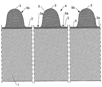
is To clarify the invention, Figure 1 in the drawing of the appendix
represents a slightly enlarged cross-sectional view of a support 1 to which a
flat first layer of silicone 2 and microstructured second layer of silicone 3
have
been applied, respectively. As one can see, the first and second layers 2 and
3 and support 1 are adhered together to form a unitary three-dimensional
2o microstructure 4. This microstructure 4 comprises a plurality of crests or
ridges that consist of the microstructured layer 3 fixed to support 1 via the
first
layer 2. Together the first silicone layer 2 and the second silicone layer 3
form
a continuous siliconized surface 5 on support 1.The siliconized surface 5 has
anti-adhesive properties which extend from bottom zones 5a continuously
2s over crest zones 5b to provide a surface adapted to release a substrate in
contact therewith. The plurality of crests or ridges are preferably
distributed
evenly over the siliconized surface 2a of the support 1, and facilitate the
separation of a substrate film (see Fig. 7) with or without adhesive which
will
have been deposited on the microstructured silicone.
CA 02548651 2006-06-07
WO 2005/063464 PCT/BE2005/000001
-15-
The following tests and examples better illustrate the invention although
they in no case limit it.
'bests on a pilot installation
The materials used, the operating conditions and the results of the tests
s are given in Tables 1 and 2 below.
1. Coating of a "grid" of silicone on presiliconated paper
The coating of the microstructured ("grid shaped") layer of silicone
is carried out by "inverse" engraving, that is by pyramids on the table of the
cylinder. These pyramids may have a truncated shape or be similar to a
to pyramid having its apex removed in a cylindrical fashion.
Characteristics of the engraving (see Figure 2a: plan view of the
engraving, and Figure 2b: cross-sectional view along line Ilb).
Cylinder No. 58472 chrome coated
Depth: 0.050 mm.
is Opening: 0.100 mm
Diagonal measurement of the pyramid: 0.500 mm.
Bottom: 0.015 mm.
The filling of the engraving is carried out~either using a closed chamber
equipped with doctor bars, or by immersion of the engraving in the silicone
2o bath, where the excess silicone on the surface of the engraving is then
eliminated with a doctor bar (made of steel, nylon or any other material). The
fixation of the microstructured layer of silicone is carried out using a
battery of
mercury UV lamps with average pressure and a power of 200 Wm.
CA 02548651 2006-06-07
WO 2005/063464 PCT/BE2005/000001
- 16 -
a
r
U O +~ - ~ . ~ . ~ . a
cC3 V O O O O O
O
_
U -~ N
L L L L L
O OO. O N N N _N
C~L
Q . ~ ~ (~ _
'~ (~ ~' ~ ~ ~ O
O
O
_ ~ C C C C
4-- O O Cff _(6 _(~5 _(B _C6
\ Q. ~ ~ ~ ~
~ O ~ Q- Q. Q. Q.
O U
fn O L ~.... '1-i .t~ Y
O O L ._ ,y.r O O Q~ N
L O
4-- ~ O
O ~ ~ ~ ~ O O
O O O O
O O O O (LS
U U U U
~ ~ ~ ~ O
I-
~<
f- ~ ~- <n cn fn fn n
a~ U F- I- F- I-
O O
C_ C_
.
s.. O ~ ~ N N
N N ~ O
O O
O :~.
Q C O a' O- U U U
Q' ; .~ U
. U ~, +~ -, O O O
- .+~ U U .L ' ' '
U -~-1
4-
~C Cn p~ ~ ~ ~ ~ ~ t
~ ~ ~
V ~ fn ~ _ Cn ~ ~ N.
Cn ~~
Q
.
'a
L
N
O ~
O
L
'G N
L~' ~ O
~I L L L. L L L L
~
L ' ~ ,~ ~ .Q ~ ~ .Q
N
N d' d' d' ~h d'
r O
d . N N N N N N
.QO O O ~ ~ ~ 0
~ C
.;~
_ N E E E E E E
~ z
~ o 0 0 0 0 0
c N N N N
N N V V V V
V V
O
O (n ~ ~ D y O ~ O
L L C7 l '
N
_
in in in
~ U Q Q ~ ~ O
V ~ ~
G >, O O O O O O O
_ OU ~ U~ 000 C~ 000U~ a00U~ op0 C~ 000~ cN-
.- c~f N II N IIN IIN II N II(> II
U O O O O O O O O O O p_,O
~
p W ~ d7 ~ 07 ~ ~
U
~
~ ~ ~ >
C
O ~ ~ ~ U d'
"'J
f/~ ~ fn '. M ~ M
N r r
O r fn r ~ _f/~ ~- O r- O
.
O' U Ill U ~ U W U C U ~ U
O ~
Q o (a , (~ C15
V ~ ~ p N
_ ~ ~ M ..QO ~ ~ .O
~
U C C C C p C C
CO M
O O C
O
Q- fn ~' fn ~ (n ~ (n ~ (n ~ fn
f~
N
I- ~- N M d' ~ CO
SUBSTITUE SHEET
CA 02548651 2006-06-07
WO 2005/063464 PCT/BE2005/000001
-17-
* The Brookfield viscosity of the silicones was measured (spindle 4,
speed 20 rpm), unit the centipoise = one mPa.s.
1 ) Signback 13 is a sized paper with kaolin of 130 g/m2.
2) R630GE (SS) is a mixture of polyorganosiloxanes with Pt catalyst,
s without solvent.
3) UV902G (+CRA 709) is a mixture of polyorganosiloxanes comprising
acrylate functions, and it is placed in the presence of 2-hydroxy-2-
methyl-1-phenylpropanone as photoinitiator, from the company
Goldschmidt.
l0 4) UVPC 900 RP is a mixture of polyorganosiloxanes comprising acrylate
functions, and it is placed in the presence of 2-hydroxy-2-methyl-1-
phenylpropanone, from the company Rhodia.
5) UV 9026 is a mixture of polydimethylsiloxanes functionalized with
acrylate function and of 2-hydroxy-2-methyl-1-phenylpropanone from
is the company Goldschmidt.
2. Coating of the adhesive
Formulation of adhesive used:
Acrylic copolymer in solution in a mixture of organic solvents: 17 kg.
2o Butyi acetate (principal solvent): 2.8 kg.
Crosslinking agent: 0.160 kg.
Drying temperature profile: 60°C, 80°C, 100°C,
120°C.
Coating speed: 20 m/min.
Gram weight of the adhesive: 20-25 g/m~.
CA 02548651 2006-06-07
WO 2005/063464 PCT/BE2005/000001
-18-
Table 2: Coating of the adhesive
Example Adhesive Face Results
No. (appearance)
1 Acrylic copolymer M8129'~ Acceptable spreading
in of
solvent the adhesive
2 Acrylic copolymer M8129 Good spreading of the
in
solvent adhesive
3 Acrylic copolymer M8129 Good spreading of the
in
solvent adhesive
4 Acrylic copolymer M8129 Acceptable spreading
in of
solvent the adhesive
1 ) M8129 is a sheet of glossy white PVC having a thickness 90 pm.
One can thus see that the coating of a silicone relief via so-called
s inverse engraving yields excellent results.
Figure 3 is a scanning electron micrograph of the microstructured
surface of silicone of Example No. 2 according to the invention (magnification
X 15 and X 30).
Figure 4 is a scanning electron micrograph of the microstructured
to surface of silicone obtained by a known method of the prior art.
According to this known method, the layer of silicone, deposited on the
glossy face of the polyethylene film of a two-faced polyethylenated paper, is
microembossed with heating (110°C) and at low speed (0.9 m/min) by an
engraved cylinder; the counter cylinder is a silicone rubber roller which has
a
CA 02548651 2006-06-07
WO 2005/063464 PCT/BE2005/000001
-19-
Shore hardness of 85 and is heated at 120°C; the pressure exerted
between
the two cylinders is 22 N/mm2.
As one can note, the inventive microstructured support has on the
surface of the silicone (Figure 3) very regular features which are rounded at
s the level of the crests, which prevents or reduces the possility of transfer
of
the image of the silicone pattern to the surface of the substrate e.g. a
flexible
film of PVC, that is there is no alteration in the surface appearance of the
substrate film. This is not the case with the micro-honeycombs of Figure 4,
where the surface of the substrate PVC film is altered by the microstructures
to of the polyethylenated and siliconated paper whose embossed crests are
much sharper and less rounded; the micro-honeycombed pattern is visible
through the PVC film which the crests deform. To ameliorate this pattern
transfer through to the substrate, the prior art may use a thicker substrate
to
lessen or blunt the image transfer. Advantageously, preferred embodiments
is of the present invention use rounded microstructured crests or ridges which
lessen or prevent silicone crest pattern transfer through to a substrates
distal
surface. Thus, the microstructured support of the present invention may by
inverse replication define the topography of the adjacent proximate surface of
the substrate while not transferring a visible (to the naked eye) image
through
2o to the distal surface of the substrate. This means that use of thinner
substrates or facestocks may be possible e.g. 60 im, 50im, or 40 im or less
may possibly be used thereby effecting a material cost savings since it is
unnecessary to use an added thickness to lessen the visual effect caused by
using a patterned silicone liner having sharp crests.
2s Other tests and test results are given in Tables 3 and 4 below.
1. Coating of a grid of silicone on presiliconated paper
The operating procedure is substantially the same as the one used above.
CA 02548651 2006-06-07
WO 2005/063464 PCT/BE2005/000001
- 20 -
_ o ~ o .a? o .a? o ~
N L ~ L ~ i.~ L-
U N Q. N Q. O Q. N Q
(B
t''~nN t~l~~ a N ~ N
t~cL3 c6 O ~ O c0O ctfO
N N . U_ .LU ~ U .,.~'..U
I1' ~ : ~ : :
Q. (~ vi a5tn t~<n (a cn
O O O O O O O O
I--~ f--s I-..
O
C C C
_ O 0~..O ~ Q. O
_ U .a-~U +.~U U .~-~U
w ~
O)O
'>O c
I5
L, (LS _
L L. L L ~ -O
.Q ..Q O
O
O >
O U
Q. O
2 O N N ~ 43
N cn Q
V V V V
U
"a~ V7 X ~ O
(n
O
~ ~ C~ C7 C~ C~ j, _a, ~ c-
' a~
' N N N N
O O r-
U > > ~ ~ c~
L ~ N
.-. ~ X i-
O N
~ ... ~ ~ ~ ~ ~ .E N
N o ~ ~ O
f~ ~ ~ (L ~ ~- U 00
~ .n -nV ~ ~ ~ o
.v~ p c~ p~ N ~ cMO Li~
c~ ~ c E...
N
N
I~ e- N M 'd'
SUBSTITUE SHEET
CA 02548651 2006-06-07
WO 2005/063464 PCT/BE2005/000001
-21 -
2. Coating of the adhesive
Formulations of adhesive used:
1. MP 500 (Solucryl 340: acrylic copolymer in solution in a mixture of
organic solvents).
s Gram weight: 24.5 g/m~
Viscosity: 135 cps (spindle 4, v20, Brookfield)
Drying temperature profile: 70°C, 90°C, 110°C,
140°C.
Coating speed: 10 m/min.
2. MR 980 (Solucryl 615: aciylic copolymer in solution in a mixture of
to organic solvents).
Gram weight: 16 g/m2
Viscosity: 790 cps (spindle 4, v20, Brookfield)
Drying temperature profile: 70°C, 90°C, 110°C,
190°C.
Coating speed: 20 m/min.
CA 02548651 2006-06-07
WO 2005/063464 PCT/BE2005/000001
-22
Table 4
Coating of the adhesive
Example PresiliconatedSiliconeAdhesiveFace Results
No.
paper (appearance)
Reference SIGNBACK 13 / MP500 M9829 Good coating
A of
UV PC900RP polymer the adhesive
75p
SIGNBACK 13 UV902G MP500 M9829 Good coating
of
R630GE (SS) the adhesive,
a
few bubbles
6 SIGNBACK 13 UV902G MP500 M9829 Good coating
of
UV PC902G the adhesive,
very
few bubbles
7 SIGNBACK 13 UV902G MP500 M9829 Good coating
of
UV PC900RP the adhesive,
a
few bubbles
8 SIGNBACK 13 UV902G MP500 M2629 Good coating
of
UV PC900RP polymer the adhesive,
60p a
few bubbles
9 SIGNBACK 13 UV902G MP500 M2629 Good coating
of
R630GE (SS) the adhesive,
a
few bubbles
SIGNBACK 13 UV902G MP500 M2629 Good coating
of
UV902G the adhesive,
very
few bubbles
11 PET 28p treatedUV902G MP500 BOPP 58p Good coating
of
RF310RP (1,6) clear the adhesive,
very
few bubbles
Reference SIGNBACK 13 / MP500 M2629 Good coating
B of
UV PC900RP the adhesive
Reference SIGNBACK 13 / MR980 M2629 Good coating
C of
UV PC900RP the adhesive
12 SIGNBACK 13 UV902G M2629 Good coating
of
R630GE (SS) the adhesive,
very
few bubbles
13 UV902G UV902G MR980 M2629 Perfect coating
of
CA 02548651 2006-06-07
WO 2005/063464 PCT/BE2005/000001
-23-
the adhesive,
no
bubbles
14 SIGNBACK UV902G MR980 M2629 Good coating
13 of
UV PC900RP the adhesive,
very
few bubbles
15 SIGNBACK UV902G MR980 M9829 Good coating
13 of
UV PC900RP the adhesive,
very
few bubbles
16 SIGNBACK UV902G MR980 M9829 Good coating
13 of
R630GE (SS) . the adhesive,
very
few bubbles
17 SIGNBACK UV902G MR980 M9829 Perfect coating
13 of
UV902G the adhesive,
no
bubbles
Reference SIGNBACK / MR980 M9829 Good coating
D 13 of
UV PC900RP the adhesive
One notes that even with a very thin substrate facestock (face) of
flexible PVC film of 60 pm thickness (M2629), one does not see the
silicone pattern image transferring through.
s Tests of industrial application
1. Coating of silicone with "inverse" engraving, and polyester
doctor bar.
The material used, the operating conditions and the results of the
tests are given in Table 5 below.
io The coating of the microstructured layer of silicone is thus carried
out by inverse engraving, that is by pyramids on the table of the cylinder.
Characteristics of the engraving:
Cylinder chrome coated
Depth : 0.050 mrn
is Width : 530 mm
Opening : 0.100 mrn
Diagonal measurment
CA 02548651 2006-06-07
WO 2005/063464 PCT/BE2005/000001
-24-
of the pyramid : 0.500 mm
Bottom : 0.015 mm
The fixation of the microstructured layer of silicone is carried out
by using 2 Hg arc-lamps with a power of 120 W/cm under an irierting
s atmosphere of N2 (<20 ppm of 02).
CA 02548651 2006-06-07
WO 2005/063464 PCT/BE2005/000001
- 25 -
0
N
4- 4- N
O O 4-
U O O _
~ ~ O
O N N O Q'
\ tin~ v
N ~ ~
N N C C C
C C C
O ~ N N
V V
N ~ ~
~ N
O O O O
_
f- H F- Q
C fn
N Q
p ~ N N ~ ~ V
O O N N
O
_ _
~
s. ~ ~ x
L N fn V1
V N ~ UO (0 to (~
~
Q _ \
Q~ L L
O
L
O
~/
~ E E
-a ~ ~ z \
N N N '
V V V L V
U
-a ~ o
O ~
.Q ~ O O O O
~ '
~ ~ d
H~ (n
O
N N N N
N ~
Q.
.
Q ~ U U U p O fn
U O O O O
=U =U -U .U cn
nt ~ ~ tnD~o ~o ~o
Q
co co co c~
fY ~ 'v
~
~
N
n N N x
O ~ ~ ~ ~' Cn
O ~ f
U~ ~7 pp ~ = n
= r- Cflfn
U
C
j ~ = = ~ ~
N N N N
; ~ ~ ~ ~ ~
. U
~ ~ ~ ~ ~ _
_
(n "t_S
'
~
a d d. I1 CL II
a ~ ~ M M
V
u- >~ > j~ ~
~ j
a. o- a a. p N
~ ~
0
o ~ p o
O ~- N M
O
I- O
SUBSTITUE SHEET
CA 02548651 2006-06-07
WO 2005/063464 PCT/BE2005/000001
-26-
2. Coating of the adhesive
Formulation of adhesive used
Resin : Solucryl 360 AB (acrylic copolymer); 720 kg
Solvent : Butyl acetate; 150 kg
s Crosslinking
agent : mixture of 2-pentanedione (1.5 kg), 3-isopropanol
(0.8 kg), Ti acetyl acetonate (0.188 kg) and AI acetyl
acetonate (2.02 kg).
Viscosity : 1300 cps (spindle 4, v20, brookfield).
to One ...... can thus see from Table 6 that like in the case of the
tests on pilot installation the coating is carried out under excellent
conditions, the adhesive performances and anti-adhesive values being
substantially lower than those obtained with control test.
CA 02548651 2006-06-07
WO 2005/063464 PCT/BE2005/000001
C
N
ctat'-'~ '~ c.~Q N c
N ~- O N ~
r
N
N tli
ct7 0~ d' h~
N O ltd r N N
O d CJ O
cY7CL
,,.,
t~
t~f
V O
t
i~. C~fl ~U 0~0
L ~ ~ Q ~ r r r r
(t~~ U ~ ,C
t~fG~ C
H
t~C~ d' cue!st'
~ O ti'3t(7ti7
r N r r r
a
a 'taa
,.c c" r ~ .r
,~-..cn ct~
N r
r r r
U
4-
N ~7 C57~7 ~~'3
> c c c
U U U U
O O Q O
~7 ~ ~ ~'3
O
w - ~ N cr3d'
U
v-,
SUBSTITUE SHEET
CA 02548651 2006-06-07
WO 2005/063464 PCT/BE2005/000001
-28-
Figure 5 is a scanning electron micrograph of the microstructured
surface of silicone (top left side) and of an inversely replicated adhesive
(bottom right side) obtained according to the method of the invention on
industrial application (60 x magnification with a 68°tilt).
s Like in the case of the tests on pilot installation one can note that the
microstructured crests are very smooth and the conjunction of rounded
crests and of relatively small crest depth of about 10 pm, cooperates to
greatly reduce and even prevent the visible transfer of the microstructured
silicone pattern to the distal surface of the adhesive coated substrate of the
to flexible film of PVC. Advantageously, crest or ridge depths less than 15 pm
may be used to help lessen or prevent the undesirable visual effect.
Figure 6 is a scanning electron micrograph of the initial contact
topography between the adhesive surface and the surface of the substrate
support which receives the self adhesive film microstructured according to
is the method of the invention. As one can clearly note from this micrograph,
and more particularly from the plate crest bordered and divided into four
squares of the same surface, the percentage of initial contact area may be
made substantially lower than the values obtained with the microstructured
adhesives known to date, which are higher than 35%. Here, the contact
2o area is about 25%. Depending on the appearance of the adhesives used,
the composition thereof and the processing conditions, the percentages of
initial contact surface between the adhesive layer and the substrate support
may vary and in one preferred embodiment are from 15 to 32%, and
preferably of 23 to 28% of the total covering surface. In these preferred
2s embodiments this low level of contact surface allows for better
repositioning
properties of the adhesive film than the adhesive films of the prior art, in
conjunction with good adhesion between the surface of the substrate and a
supporting object to which it is applied, because the adhesive surface at the
top of the crests is substantially planar and will give by microreplication a
CA 02548651 2006-06-07
WO 2005/063464 PCT/BE2005/000001
- 29 -
plane microplateau. Furthermore, the presence of so formed
microchannels of small depth (of about 10 pm) and the high immediate non
contact adhesive surface (of about 70% or more) provides to the self
adhesive product a repositionable character in the case of the initial
s application pressure is low. Now, if a higher pressure is exerted upon the
applied adhesive film, said film is immediately fixed to the surface of a
supporting object because all the planar surfaces of the crests of adhesive
in the form of plane plateaux are then in full contact with the object
surface.
The microchannels formed by the adhesive contact with the object surface
~o and circumscribed by the object surface and the substrate's immediate non
contact adhesive surfaces have a depth which allows an easy egress and
elimination of the pockets of air which could occur at the interface of
adhesion during the application of the self-adhesive product. The simple
contact of the hand on the locations where the pockets of air are formed
is can cause the rapid and complete suppression or expulsion of these
pockets of air. If a greater pressure is then exerted, the plane surfaces of
the different plateaux of adhesive can extend substantially to the plane
valleys of the first layer of silicone depending on the exerted pressure, the
viscoelasticity properties of the adhesive, the time and the temperature to
2o coalesce infio a uniform and continuous surface (without the original
microchannels) in close contact with the application(object).
Figure 7 is a diagrammatic representation in two dimensions of the
process of the invention showing a presiliconised support (1, 2) on which a
microstructured silicone layer 3 has been applied, hardenable by ultraviolet
2s radiation, as well as an inverse replicated three-dimensional
microstructure
obtained on the adhesive layer 10 of substrate l1when contacting the latter
with the presiliconized liner (1,2) and the microstructured Payer 3, and also
a
substrate 11 having a facestock 12.
CA 02548651 2006-06-07
WO 2005/063464 PCT/BE2005/000001
-30-
As shown, one can note that the percentage of adhesive surface
which will be immediately in contact with the surface on which the self-
adhesive film will be applied is 27 %, this percentage being calculated as
follows
s Distance AB = 237 pm
Distance BC = 216 pm
s/S = 2372 = 0.27
(237 + 216)2
It should be also noted that the adhesion interface between the adhesive
io surface and the application surface is substantially planar because it
corresponds to the valleys formed by the first flat layer of silicone of the
three-dimensional microstructure.
Besides the already detailed advantage that one may obtain a
microstructured surface of silicone on any type of substrate, such as a
is cellulosic or noncellulosic paper (calendered or glossy, sized), plastic
films
e.g. polyester, polyolefin, polyethylene, polypropylene, polyamide (uniaxially
or biaxially oriented or unoriented, monolayer or multilayer, with or without
printing or designs, colorants, processing aids, fillers and the commonly
known additives) and the advantage that one can coat the silicone on a
2o support web at a very high speed e.g greater than 10
meters/minute(m/min), and preferably greater than 50 and even
300 m/min, the principal advantages of the microstructuring method of the
invention are that one may obtain extremely regular microstructured motifs
whose crests may be configured (e.g. small height and rounded) so as to
as not deform the substrate film (or facestock) on which the microreplicated
surface of adhesive is applied.
The principal use of a microstructured adhesive is that it makes it
easy to apply, for example, large emblems on given surfaces. Indeed, in
general one has to remove and reapply the emblem to position it better
CA 02548651 2006-06-07
WO 2005/063464 PCT/BE2005/000001
-31-
and, once it is applied, one often has to eliminate pockets of air caught
under the self-adhesive film during the application or pockets of gas which
occur sometime after the application. The microstructured adhesive
according to the present invention allows easy repositioning, easy
s elimination of bubbles during the application by simply applying manual
pressure e.g. with one or more fingers or a hand, and it allows the
elimination, through the microchannels formed, of any gas which may have
been enclosed after the application.
It will be apparent from the foregoing that various inventive articles
to may be formed according to the present invention including a novel release
liner, a novel pressure sensitive adhesive label having a release liner and
that such articles may be employed in a wide variety of applications
including in the production of very large graphic panels suitable for
placement on buildings, vehicles and billboards. Such large graphic panels
is may have a width of 30, 50, 100 or 150 cm or more with a length usually at
least as long or often 1, 2, 3 or many meters more in length. Such panels
or sheets may often have a thickness of 1.25 millimeters(mm) or less.
One preferred embodiment of the invention is a multilayer sheet
comprising:
20 (a) a flexible support comprising:
(i) a sheetlike structure having a first broad surface and opposing
second broad surface;
(ii) a first layer of a silicone containing material e.g. in a sheetlike
coating that is fixed to at least the first broad surface of the
aforementioned
2s sheetlike structure;
(iii) a second layer of a silicone containing material fixed to the first
layer (ii) as a plurality of ridges or crests thereby providing a flexible
support
having on at least one broad surface thereof a three dimensional
topography of a plurality of ridges or crests; and
CA 02548651 2006-06-07
WO 2005/063464 PCT/BE2005/000001
-32-
(b) a flexible substrate having a proximate first surface and opposing distal
second surface wherein the proximate first surface is in releasable contact
with the three dimensional surface of the flexible support and the proximate
first surface has a mating inversely replicated three dimensional
s topography.
The sheetlike structure of the flexible support is preferably not
distorted into a plurality of ridges or crests corresponding to the second
layer ridges or crests e.g. by embossing. Advantageously, the distal
second surface of the flexible substrate is visually free from any ridge or
z0 crest pattern corresponding to the plurality of ridges or crests of the
flexible
support. The substrate may comprise a first adhesive layer forming a
proximate first surface of the substrate. and may optionally further comprise
a first facestock layer in contact with the first adhesive layer and the
facestock layer forming an opposing distal second surface of the substrate.
is The distal substrate surface may be printed e.g. using inks, pigments or
colorants, with one or more images, indicia or designs or it may be
unprinted, transparent, opaque, translucent, black, white or colored, either
in part or over its entire surface. The distal surface of the substrate may
also optionally have an additional exterior protective coating or layer
applied
2o thereto.
It should be understood that the invention is in no way limited to the
described embodiments and that many modifications can be made to the
latter without exceeding the context of the present patent.