Note: Descriptions are shown in the official language in which they were submitted.
CA 02548737 2006-06-08
WO 2005/061955 PCT/US2004/032316
TITLE OF THE INVENTION
HIGH FLUX LIGHT EMITTING DIODE (LED) REFLECTOR ARRAYS
DISCUSSION OF THE BACKGROUND
FIELD OF THE INVENTION
The present invention is directed to reflectors to utilize with light emitting
diodes
(LEDs), and particularly when the LEDs are high-flux LEDs.
DISCUSSION OF THE BACKGROUND
High-flux LEDs are becoming more and more prevalent. A high-flux LED is
generally an LED with greater luminous output in comparison with earlier
developed
traditional 5 mm LEDs, and an LED that has a larger size chip than in the
traditional 5 mm
LED. A high-flux LED for the purposes of this disclosure is defined as an
individual LED
package that is capable of dissipating more than .75 watts of electric power.
With
improvement in high-flux LED technology, more and more companies are
developing
different types of high-flux LEDs. High-flux LEDs also typically have larger
viewing angles
in comparison with a traditional 5 mm LED. To use such high-flux LEDs
efficiently,
mechanisms have been provided to redirected light output from the larger
viewing angle of
the high-flux LEDs. One known way to use the light output from high-flux LEDs
more
efficiently is to use a reflective/refractive lens to redirect output light.
That approach has
been utilized by companies such as Lumileds, Osram, and Fraen, etc.
SUMMARY OF THE INVENTION
However, the applicants of the present invention recognized that a significant
drawback exists in utilizing such a reflective/refractive lens. Such a
reflective/refractive lens
is a plastic lens, and one major drawback of utilizing such a plastic lens is
that the lens is
usually very bulky. That results in limiting the LED packing density and makes
the LED
difficult to mount.
Accordingly, one object of the present invention is to address the above-noted
and
other drawbacks in the background art.
CA 02548737 2006-06-08
WO 2005/061955 PCT/US2004/032316
Another object of the present invention is to provide novel reflectors to be
utilized
with LEDs, and which may find particular application with high-flux LEDs. Such
novel
reflectors are small in size and easy to utilize.
BRIEF DESCRIPTION OF THE DRAWINGS
A more complete appreciation of the present invention and many of the
attendant
advantages thereof will be readily obtained as the same becomes better
understood by
reference to the following detailed description when considered in connection
with the
accompanying drawings, wherein:
Figures la-lc show a first embodiment of the present invention;
Figures 2a-2c show a further embodiment of the present invention;
Figures 3a-3g show a further embodiment of the present invention;
Figures 4a and 4b show specific implementations of embodiments of the present
invention;
Figure Sa shows a detailed view of a reflector of an embodiment of the present
invention;
Figure Sb shows results achieved by the embodiment of Figure Sa;
Figure 6a shows a detailed view of a reflector of a further embodiment of the
present
invention;
Figure 6b shows results achieved by the embodiment of Figure 6a;
Figure 7a shows a detailed view of a reflector of a further embodiment of the
present
invention;
Figures 7b and 7c show results achieved by the embodiment of Figure 7a;
Figure 8a shows a detailed view of a reflector of a further embodiment of the
present
invention;
Figures 8b and 8c show possible results achievable by the embodiment of Figure
8a;
Figure 9a shows a further embodiment of a reflector structure of the present
invention;
Figure 9b shows results achieved by the embodiment of Figure 9a;
Figure 10 shows details of a further embodiment of the present invention;
Figures 11 a-11 c show views of further embodiments of the present invention;
Figures 12a and 12b show a modification of a reflector structure of the
present
invention;
Figures 13a and 13b show a further modification of a reflector structure of
the present
invention; and
2
CA 02548737 2006-06-08
WO 2005/061955 PCT/US2004/032316
Figures 14a andl4b show a further modification of a reflector structure of the
present
invention.
DESCRIPTION OF THE PREFERRED EMBODIMENTS
In the following description to the drawings, like reference numerals
designate
identical or corresponding parts throughout the several views.
As discussed above, the applicants of the present invention recognized that
high-flux
LEDs typically have larger viewing angles in comparison with traditional 5 mm
LEDs, and
that a background approach to utilizing a reflective/refractive lens to
redirect light from plural
lugh-flux LEDs has a drawback in making an overall light device bulky and
difficult to
mount.
To address such drawbacks in the background art, the present inventors
realized that
enhanced packing density and mountability could be realized by utilizing a
reflector for LEDs
in which each LED, or at least a group of LEDs, fits into its own reflector
portion. Such a
structure allows high redirection of light from each individual LED in a
device that is not
very bulky and that is not difficult to mount. The present invention is
particularly applicable
to high-flux LEDs because high-flux LEDs have large viewing angles. Further,
high-flux
LEDs are typically utilized in systems in which fewer LEDs are provided,
making it more
feasible to provide an individual reflector for each LED.
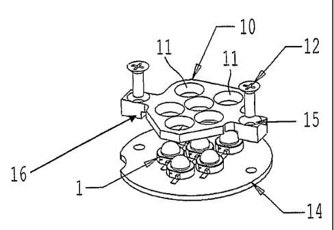
A first embodiment of the present invention is shown in Figures la-lc.
As shown in Figures 1 a-1 c a plurality of high-flux LEDs 1 are mounted onto
an LED
printed circuit board 14. In the embodiment shown in Figures la-lc a master
reflector device
having individual reflecting portions or reflectors 11 is provided. Those
individual
reflectors 11 are provided to each surround one respective high-flux LED 1.
That is, in this
embodiment of the present invention each LED 1 is surrounded by a respective
reflector 11 of
the master reflector device 10.
As shown most clearly in Figure lc, each individual LED 1 fits inside an
individual
reflector 11 and walls of the reflector 11 are sloped with respect to the LED
1. That allows
light output from sides of the LED 1 to be efficiently reflected. High-flux
LEDs have a large
viewing angle, meaning that they emit a larger amount of light in divergent
directions. By
utilizing the master reflector 10 of Figure 1 light can be reflected by the
sloped walls of the
individual reflectors 11, which light would otherwise not be viewed.
The reflector device 10 may be made of molded plastic and may have an aluminum
coating coated on the reflective wall surfaces of the individual reflectors
11. With such a
3
CA 02548737 2006-06-08
WO 2005/061955 PCT/US2004/032316
structure the reflective surfaces can reflect a portion of light from each
individual high-flux
LED 1 that would otherwise be lost.
As shown in Figures la-lc, the master reflector device 10 also includes holes
15
through which mounting screws 12 are passed to mount the master reflector 10
to the LED
printed circuit board 14. Further, the master reflector device 10 includes a
step 16. The size
of the step 16 is chosen so that when the master reflector 10 is mounted on
the LED printed
circuit board 14, each individual reflector 11 is at the appropriate height
relative to the LED 1
surrounded by the individual reflector 11. Figure lc specifically shows from a
side view the
mounting of the master reflector 10 so that each individual reflector portion
11 is at the
appropriate height relative to each high-flux LED 1.
Figures 2a-2c show a further embodiment of the present invention, which shows
a
master reflector 20 of a different shape and with a different mounting
structure. In the
embodiment of Figure 2 the master reflector 20 is not mounted to the LED
printed circuit
board 24 by the screws 22 passing through holes 25, but instead the master
reflector 20 is
mounted to receptacle portions 26 in a lamp housing.
A further implementation of an embodiment of the present invention is shown in
Figures 3a-3g. Figures 3a-3g show an embodiment of how the master reflector
device of the
present invention can be specifically incorporated into an LED light device
including a lens
and the LEDs. In that further embodiment of Figures 3a-3g, the system
combining the LEDs,
and the reflectors includes heat stake features to allow the reflector to be
assembled to a lens
prior to the LED sub-assembly. Once the lenslreflector sub-assembly is
complete, then the
LED sub-assembly can be assembled onto a back post of the reflector using
screws.
More specifically, Figure 3a shown a lens 35 with heat stakes 32 used for
mounting
purposes. Figure 3b shows an LED printed circuit board 34 including plural
high-flux LEDs
1. Figure 3c shows front F and back B sides of a master reflector 30 with
individual reflector
portions 31.
As shown in Figures 3d and 3e, the master reflector 30 is fit inside the lens
35 with
the heat stakes 32.
Then, as shown in Figures 3f and 3g, the LED printed circuit board 34 with the
LEDs
1, the LEDs 1 not being shown in those figures as they are on the opposite
face of the LED
board 34 (i.e. Figures 3f and 3g show the back side of the LED board 34), are
then fit into the
assembly shown in Figure 3e, so that each individual LED 1 is fit inside one
of the individual
reflectors 31. The overall assembly is then assembled by screws 32.
4
CA 02548737 2006-06-08
WO 2005/061955 PCT/US2004/032316
Such a further embodiment allows the master reflector 30 to be fit into the
lens 31
prior to the LED printed circuit board 34 being fit thereto.
By utilizing the embodiment of Figures 3a-3g, benefits in a manufacturing
operation
can be achieved. Specifically, utilizing the embodiment of Figures 3a-3g
allows a pre-
assembly of the lens 35 to the reflector 30, and as a result if desirable an
additional heat sinlc
can be assembled to the LED board 34 and not to the lens 35. With that
structure the lens 35
can be used for a mounting application.
The reflector structures noted in each of the embodiments of Figures 1-3 are
applicable to different types of LEDs. As examples only, the reflector
structures may be
utilized with Lumileds Luxeon type package LEDs such as shown in the
embodiment of
Figure 4a, or may also be utilized with surface mounted type package LEDs such
as Osram's
Golden Dragon LEDs, such as shown for example in Figure 4b. Another example of
high-
flux LEDs is Nichia's NCCx-series LEDs.
Further, in the embodiments shown in Figures 1-3 the shape of each individual
reflector 11, 21, 31 can be symmetrical to the optical axis of the individual
LEDs 1, although
an unsyrmnetrical shape can also be realized, as discussed in a further
embodiment below.
Further, and as shown for example in Figure Sa, the cross-section of each
individual
reflector 11, 21, 31 may be conic. When utilizing an individual reflector 11,
21, 31 with a
conic cross-section as shown in Figure Sa, the output light distribution may
have an angular
distribution such as shown in Figure Sb.
As another possible shape of each individual reflector 1 l, 21, 31, each
individual
reflector 11, 21, 31 may have a cross-section of a complicated curve as shown
for example in
Figure 6a. When utilizing individual reflectors 11, 21, and 31 with such a
shape of a
complicated curve as shown in Figure 6a, the output light distribution takes
the form shown
in Figure 6b.
In each of the reflecting surfaces shown in Figures Sa and 6a, a portion of
the light
output from the high-flux LED 1 propagates to the reflective surfaces of the
individual
reflectors 11, 21, 31, and the light is reflected to a direction closer to the
optical axis of the
LED 1. Other portions of the light output from the LED 1 are not interfered
with by the
reflectors 11, 21, 31 and travel uninterrupted. The divergent angle of the
light can be
changed by changing the slope or curvature of the reflective surfaces and the
height of the
reflectors.
CA 02548737 2006-06-08
WO 2005/061955 PCT/US2004/032316
Different modifications of the cross-section of each individual reflector 11,
21, 31 can
of course be implemented, particularly between the two noted shapes in Figures
Sa and 6a to
achieve any desired light output.
As shown in Figure 7a, the shape of each individual reflector may also be that
of an
oval. With that shape light as shown in Figures 7b and 7c are output. As shown
in Figure 7b,
by utilizing an individual reflector 11, 21, 31 with an oval shape an
isotropic angular intensity
distribution of the output light can be realized. Further, Figure 7c shows the
typical angular
intensity distribution when utilizing an oval shape individual reflector 11,
21, 31. With such
an oval shape the light divergent angles in the two directions perpendicular
to the LED axis
are different, thereby resulting in an oval shape distribution.
In the embodiments noted above the individual reflector portions 11, 21, 31
are
substantially shown as symmetrically shaped with respect to an optical axis of
light output by
the surrounded LED 1. However, as shown for example in Figure 8a any of the
individual
reflector portions 1 l, 21, 31 can be shaped unsymmetrically, i.e. offset from
an axis of light
output from each individual LED 1.
Further, when utilizing unsymmetrically shaped LEDs the individual reflectors
of a
multi-reflector-device do not have to be identical. As an example, each
individual reflector
could be tilted at an angle, which slightly differs from the angle of tilt of
other individual
reflectors. Figures 8b and 8c provide examples of how such a feature can be
utilized to
obtain a desired light output. Figure 8c shows light output from three
adjacent LEDs in.
which each of the adjacent LEDs is non-tilted. Because each LED is non-tilted
the light
output from each LED will differ, and as can be seen in Figure 3c three
"rings" of output light
are realized that are not congruent.
However, if it is desired that the light output from three adjacent LEDs are
to be
superimposed upon one another, then the three LEDs can be tilted so that the
three "rings" of
output light could be shifted to overlap and approximate a light output of one
more powerful
LED, as shown for example in Figure 8b. Utilizing such a feature can be
important in signals
and lamps with a secondary optic in the range of the light-sources near field.
In that
environment, by tilting the reflectors from adjacent LED the light can be
concentrated on the
secondary optic.
The individual reflectors can be tilted to be unsymmetrical with respect to an
axis of
the light output of the LED in any desired manner, and Figures 8a-8c only show
examples of
such an operation.
6
CA 02548737 2006-06-08
WO 2005/061955 PCT/US2004/032316
Each of the embodiments noted above shows each high-flux LED 1 surrounded by
an
individual reflector 1 l, 21, or 31.
However, a usage may be desired in which only one direction of a light beam
needs to
be compressed while the other direction may be preferably left unchanged. In
that situation a
two-dimensional reflector such as shown in Figure 9a can be utilized. In the
two-dimensional
reflector shown in Figure 9a a master reflector 90 includes three individual
reflector portions
911, 912, and 913. Each individual reflector portion 911, 912, and 913
surrounds plural LEDs
set forth in a linear configuration. As noted above, with such a structure
only one direction of
the light beam is compressed while the other direction is unchanged.
The typical angular intensity distribution of light output by the embodiment
of Figure
9a is shown in Figure 9b.
By utilizing the LED reflectors in the present invention light that may
otherwise not
be utilized can be effectively redirected to increase the performance of LEDs.
The applicants of the present invention have also recognized that it may be
beneficial
in any of the LED structures noted above to reduce the reflection of impinging
light, for
example from sunlight impinging on the reflectors and/or the LEDs, i.e. to
reduce the sun
phantom-effect.
With reference to Figure 10 in the present specification, a structure for
achieving that
result is shown.
Figure 10 shows the structure in which LEDs 1 are mounted on a LED printed
circuit
board 14, 24, 34, which can correspond to any of the LED printed circuit
boards 14, 24, 34 in
any of the embodiments noted above, and also with any needed modifications. A
master
reflector 10, 20, 30 with individual reflector elements 11, 21, 31 is provided
around the LEDs
1. As shown in Figure 10, in such a structure the LED board 14, 24, 34 is
mounted onto a
structure 105 with heat sink properties. Further, various electronic
components 110 for
driving the LEDs are also provided. Blank soldering joints/pads 115 are also
utilized in such
a structure to provide soldering, contact pads, etc.
In such a structure as in Figure 10 impinging light, for example from sunlight
or from
other sources, would conventionally be reflected off of the blank soldering
joints/pads 115
and electronic devices 110. However, the present invention avoids that result
by providing
light absorbing members 100 as an extension of the master reflectors 10, 20,
30. The light
absorbing members 100 extend above the electronics 110 and the blank soldering
joints/pads
115. As a result phantom light can be reduced since impinging light will not
be reflected
from the blank soldering joints/pads 115 and electronic devices 110, but
instead will be
7
CA 02548737 2006-06-08
WO 2005/061955 PCT/US2004/032316
absorbed by the light absorbing members 100. Those members 100 can be formed
of any
non-reflective material.
In the embodiments noted above each individual reflector 11, 21, 31 has sloped
walls
which can be coated with the reflective material such as aluminum. However, it
may be
desirable in each individual reflector to provide an antireflection portion to
reduce the
reflection of incident extraneous light, for example sunlight. Different
structures to achieve
that result are shown in Figures 11 a-1 lc. In each of these figures an anti-
reflection area is
provided at a portion of the reflector. That portion at which the anti-
reflection area is
provided may be a portion that is particularly susceptible to incident light,
for example to
incident sunlight. The position of the anti-reflection area will depend on
several factors such
as characteristics of secondary optics, critical angle of extraneous light,
and viewing area to
the observer. To decide where the anti-reflection area is best positioned, how
big it is, and
what form it has, one can use optical simulation software to arrive at a
theoretical solution or
one can build a prototype and take a look at where the main reflexes occur as
a practical
solution.
As shown in the specific embodiment of Figure l la a master reflector
surrounds the
LED 1. In that structure a metallized or reflective area 125 is provided on
almost all sides of
the LED 1. However an area 12d that is not reflective is also provided. That
non-reflective
area 120 can take the form of an area having a matte finish as shown in Figure
11 a, can be a
dark area 121 as shown in Figure l 1b, or can be an omitted area 122 as shown
in Figure l l c,
i.e. an area where there is no metallized area or reflective area. ~Jtilizing
any of the matte
finished area 120, dark area 121, or omitted area 122 spreads or absorbs
incident extraneous
light that otherwise would be reflected towards a viewer.
The embodiments noted above show the reflectors 11, 21, 31 as having generally
smooth walls. However, the reflectors are not limited to such a structure.
With reference to Figures 12a and 12b, the side reflective walls of any of the
above-
noted reflectors 11, 21, 31 can also include facets 120, Figure 12a showing a
side reflective
wall of a reflector and an LED 1 from a side view and Figure 12b showing the
same LED 1
and reflector from a top view. As shown in Figures 12a and 12b, the side
reflective walls of
the reflector have facets 120.
As a further feature of the present invention, the side reflective walls of
the reflectors
can be utilized to capture a portion of light output from the corresponding
surrounded LED to
provide a general indication of light being output from the LEDs. Different
embodiments of
achieving such a result are shown in Figures 13a, 13b, and 14a, 14b.
CA 02548737 2006-06-08
WO 2005/061955 PCT/US2004/032316
As shown in Figure 13a, the side reflective walls of the reflector 11, 21, 31
include a
specialized reflector zone 130. The specialized reflector zone 130 is
positioned to reflect a
small portion of light from the LED 1 specifically towards a light sensor 135.
As shown in
Figures 13a and 13b, different individual reflectors 11, 21, 31 include the
same specialized
reflector zone 130 and all output light to the same sensor .135. With such an
operation it
becomes possible to measure a defined percentage of luminance intensity of all
of the LEDs.
As shown in Figures 13a and 13b, the specialized reflector zones 130 are only
a small portion
of the reflectors 11, 21, 31 and thereby only a small amount of optical light
is lost from being
visible and is provided to the sensor 135. The light sensed at the sensor 135
can be utilized
in, for example, an intensity feedback operation.
Figures 14a and 14b show an alternative structure to achieve the same result
as shown
in Figures 13a and 13b. In Figures 14a and 14b, the specialized reflector zone
takes the shape
of a small hole 140 provided in a wall of the reflector 11, 21, 31. A small
portion of light
from the LED 1 is then passed through the small hole 140 and provided to a
sensor 135.
The above-noted structures can be applied to any or all of the reflectors 11,
21, 31,
dependent on how precise an indication of output light is desired.
Obviously, numerous additional modifications and variations of the present
invention
are possible in light of the above teachings. It is therefore to be understood
that within the
scope of the appended claims, the present invention may be practiced otherwise
than as
specifically described herein.
9