Note: Descriptions are shown in the official language in which they were submitted.
CA 02548805 1997-04-24
1
Light-controlled Electrokinetic Assembly of Particles Near Surfaces
Field of the Invention:
The present invention generally relates to the field of materials science and
analytical chemistry.
The present invention specifically relates to the realization of a complete,
functionally integrated system for the implementation of biochemical analysis
in a planar,
miniaturized format on the surface of a conductive and/or photoconductive
substrate, with
applications in pharmaceutical and agricultural drug discovery and in in-vitro
or genomic
diagnostics. In addition, the method and apparatus of the present invention
may be used
to create material surfaces exhibiting desirable topographical relief and
chemical function-
ality, and to fabricate surface-mounted optical elements such as lens arrays.
Background of the Invention
I - Ions, Electric Fields and Fluid Flow: Field-induced Formation of Planar
Bead Arrays
Electrolcinesis refers to a class of phenomena elicited by the action of an
CA 02548805 1997-04-24
2
=
electric field on the mobile ions surrounding charged objects in an
electrolyte solution.
When an object of given surface charge is inunersed in a solution containing
ions, a
diffuse ion cloud forms to screen the object's surface charge. This
arrangement of a layer
of (immobile) charges associated with an immersed object and the screening
cloud of
(mobile) counterions in solution is referred to as a "double layer". In this
region of small
but finite thickness, the fluid is not electroneutral. Consequently, electric
fields acting on
this region will set in motion ions in the diffuse layer, and these will in
turn entrain the
surrounding fluid. The resulting flow fields reflect the spatial distribution
of ionic current
in the fluid. Electroosmosis represents the simplest example of an
electrolcinetic
phenomenon. It arises when an electric field is applied parallel to the
surface of a sample
container or electrode exhibiting fixed surface charges, as in the case of a
silicon oxide
electrode (in the range of neutral pH). As counterions in the electrode double
layer are
accelerated by the electric field, they drag along solvent molecules and set
up bulk fluid
flow. This effect can be very substantial in narrow capillaries and may be
used to
advantage to devise fluid pumping systems.
Electrophoresis is a related phenomenon which refers to the field-induced
transport of charged particles immersed in an electrolyte. As with
electroosmosis, an
electric field accelerates mobile ions in the double layer of the particle.
If, in contrast to
the earlier case, the particle itself is mobile, it will compensate for this
field-induced
motion of ions (and the resulting ionic current) by moving in the opposite
direction.
Electrophoresis plays an important role in industrial coating processes and,
along with
electroosmosis, it is of particular interest in connection with the
development of capillary
electrophoresis into a mainstay of modern bioanalytical separation technology.
In confined geometries, such as that of a shallow experimental chamber in
the form of a "sandwich" of two planar electrodes, the surface charge
distribution and
topography of the bounding electrode surfaces play a particularly important
role in
determining the nature and spatial structure of electroosmotic flow. Such a
"sandwich"
electrochemical cell may be formed by a pair of electrodes separated by a
shallow gap.
Typically, the bottom electrode will be formed by an oxide-capped silicon
wafer, while
the other electrode is formed by optically transparent, conducting indium tin
oxide (ITO).
The silicon (Si) wafer represents a thin slice of a single crystal of silicon
which is doped
to attain suitable levels of electrical conductivity and insulated from the
electrolyte solution
by a thin layer of silicon oxide (Si0x).
The reversible aggregation of beads into planar aggregates adjacent to an
CA 02548805 1997-04-24
3
electrode surface may be induced by a (DC or AC) electric field that is
applied normal to the
electrode surface. While the phenomenon has been previously observed in a cell
formed by a
pair of conductive ITO electrodes (Richetti, Prost and Barois, J. Physique
Lettr. 45, L-1137
through L-1143 (1984)), it has been only recently demonstrated that the
underlying attractive
interaction between beads is mediated by electrokinetic flow (Yeh, Seul and
Shraiman,
"Assembly of Ordered Colloidal Aggregates by Electric Field Induced Fluid
Flow", Nature
386, 57-59 (1997). This flow reflects the action of lateral non-uniformities
in the spatial
distribution of the current in the vicinity of the electrode. In the simplest
case, such non-
uniformities are introduced by the very presence of a colloidal bead near the
electrode as a
result of the fact that each bead interferes with the motion of ions in the
electrolyte. Thus, it
has been observed that an individual bead, when placed near the electrode
surface, generates a
toroidal flow of fluid centered on the bead. Spatial non-uniformities in the
properties of the
electrode can also be introduced deliberately by several methods to produce
lateral fluid flow
toward regions of low impedance. These methods are described in subsequent
sections below.
Particles embedded in the electrokinetic flow are advected regardless of their
specific chemical or biological nature, while simultaneously altering the flow
field. As a
result, the electric field-induced assembly of planar aggregates and arrays
applies to such
diverse particles as: colloidal polymer lattices ("latex beads"), lipid
vesicles, whole
chromosomes, cells and biomolecules including proteins and DNA, as well as
metal or
semiconductor colloids and clusters.
Important for the applications to be described is the fact that the flow-
mediated attractive interaction between beads extends to distances far
exceeding the
characteristic bead dimension. Planar aggregates are formed in response to an
externally
applied electric field and disassemble when the field is removed. The strength
of the applied
field determines the strength of the attractive interaction that underlies the
array assembly
process and thereby selects the specific arrangement adopted by the beads
within the array.
That is, as a function of increasing applied voltage, beads first form planar
aggregates in which
particles are mobile and loosely packed, then assume a tighter packing, and
finally exhibit a
spatial arrangement in the form of a crystalline, or ordered, array resembling
a raft of bubbles.
The sequence of transitions between states of _______________________________
CA 02548805 1997-04-24
4
increasing internal order is reversible, including complete disassembly of
planar
aggregates when the applied voltage is removed. In another arrangement, at low
initial
concentration, beads form small clusters which in turn assume positions within
an ordered
"superstructure.
- Patterning of Silicon Oxide Electrode Surfaces
Electrode patterning in accordance with a predetermined design facilitates
the quasi-permanent modification of the electrical impedance of the EIS
(Electrolyte-
Insulator-Semiconductor) structure of interest here. By spatially modulating
the EIS
impedance, electrode-patterning determines the ionic current in the vicinity
of the
electrode. Depending on the frequency of the applied electric field, beads
either seek out,
or avoid, regions of high ionic current. Spatial patterning therefore conveys
explicit
external control over the placement and shape of bead arrays.
While patterning may be achieved in many ways, two procedures offer
particular advantages. First, UV-mediated re-growth of a thin oxide layer on a
properly
prepared silicon surface is a convenient methodology that avoids
photolithographic resist
patterning and etching. In the presence of oxygen, UV illumination mediates
the
conversion of exposed silicon into oxide. Specifically, the thickness of the
oxide layer
depends on the exposure time and may thus be spatially modulated by placing
patterned
masks into the UV illumination path. This modulation in thickness, with
typical variations
of approximately 10 Angstroms, translates into spatial modulations in the
impedance of
the Si/SiOx interface while leaving a flat and chemically homogeneous top
surface exposed
to the electrolyte solution.
Second, spatial modulations in the distribution of the
electrode surface charge may be produced by UV-mediated photochemical
oxidation of
a suitable chemical species that is first deposited as a monolayer film on the
SiOx surface.
This method permits fine control over local features of the electrode double
layer and thus
over the electrokinetic flow.
A variation of this photochemical modulation is the creation of lateral
gradients in the EIS impedance and hence in the current generated in response
to the
applied electric field. For example, this is readily accomplished by
controlling the UV
exposure so as to introduce a slow lateral variation in the oxide thickness or
in the surface
charge density. As discussed below, control over lateral gradients serves to
induce lateral
bead transport and facilitates the implementation of such fundamental
operations as
CA 02548805 1997-04-24
capturing and channeling of beads to a predetermined destination along
conduits in the form of
impedance features embedded in the Si/SiOx interface. Photochemical patterning
of functionalized
chemical overlayers also applies to other types of electrode surfaces
including ITO.
5 III - Light-controlled Modulation of the Interfacial Impedance
The spatial and temporal modulation of the EIS-impedance in accordance with a
pattern of external illumination provides the basis to control the
electrokinetic forces that mediate
bead aggregation. The light-modulated electrokinetic assembly of planar
colloidal arrays facilitates
remote interactive control over the formation, placement and rearrangement of
bead arrays in
response to corresponding illumination patterns and thereby offers a wide
range of interactive
manipulations of colloidal beads and biomolecules.
To understand the principle of this methodology, it will be helpful to briefly
review
pertinent photoelectric properties of semiconductors, or more specifically,
those of the EIS structure
formed by the Electrolyte solution (E), the Insulating SiOx layer (1) and the
Semiconductor (S). The
photoelectric characteristics of this structure are closely related to those
of a standard Metal-
Insulator-Semiconductor (MIS) or Metal-Oxide-Semiconductor (MOS) devices which
are described
in S.M. Sze, "The Physics of Semiconductors", 2nd Edition, Chapt 7 (Wiley
Interscience 1981).
The interface between the semiconductor and the insulating oxide layer
deserves
special attention. Crucial to the understanding of the electrical response of
the MOS structure to light
is the concept of a space charge region of small but finite thickness that
forms at the Si/SiOx interface
in the presence of a bias potential. In the case of the EIS structure, an
effective bias, in the form of a
junction potential, is present under all but very special conditions. The
space charge region forms in
response to the distortion of the semiconductor's valence and conduction bands
("band bending") in
the vicinity of the interface. This condition in turn reflects the fact that,
while there is a bias potential
across the interface, there is ideally no charge transfer in the presence of
the insulating oxide. That is,
in electrochemical language, the EIS structure eliminates Faradaic effects.
Instead, charges of
opposite sign accumulate on either side of the insulating oxide layer and
generate a finite
polarization.
CA 02548805 1997-04-24
6
In the presence of a reverse bias, the valence and conduction band edges.
of an n-doped semiconductor bend upward near the Si/SiOx interface and
electrons flow
out of the interfacial region in response to the corresponding potential
gradient. As a
result, a majority carrier depletion layer is formed in the vicinity of the
Si/SiOx interface.
Light absorption in the semiconductor provides a mechanism to create electron-
hole pairs
within this region. Provided that they do not instantaneously recombine,
electron-hole
pairs are split by the locally acting electric field, and a corresponding
photocurrent flows.
It is this latter effect that affords control over the electrokinetic assembly
of beads in the
electrolyte solution.
To understand in more detail the pertinent frequency dependence of the
light-induced modulation of the EIS impedance, two aspects of the equivalent
circuit
representing the HIS structure are noteworthy. First, there are close
analogies between
the detailed electrical characteristics of the electric double layer at the
electrolyte-oxide
interface, and the depletion layer at the interface between the semiconductor
and the
insulator. As with the double layer, the depletion layer exhibits electrical
characteristics
similar to those of a capacitor with a voltage-dependent capacitance. As
discussed,
illumination serves to lower the impedance of the depletion layer. Second,
given its
capacitive electrical response, the oxide layer will pass current only above a
characteristic
("threshold") frequency. Consequently, provided that the frequency of the
applied voltage
exceeds the threshold, illumination can lower the effective impedance of the
entire HIS
structure.
This effective reduction of the HIS impedance also depends on the light
intensity which determines the rate of generation of electron-hole pairs. In
the absence
of significant recombination, the majority of photogenerated electrons flow
out of the
depletion region and contribute to the photocurrent. The remaining hole charge
accumulates near the Si/SiOx interface and screens the electric field acting
in the depletion
region. As a result, the rate of recombination increases, and the efficiency
of
electron-hole separation, and hence the photocurrent, decreases. For given
values of
frequency and amplitude of the applied voltage, one therefore expects that as
the
illumination intensity increases, the current initially increases to a maximum
level and then
decreases. Similarly, the impedance initially decreases to a minimum value (at
maximum
current) and then decreases.
This intensity dependence may be used to advantage to induce the lateral
CA 02548805 1997-04-24
7
displacement of beads between fully exposed and partially masked regions of
the interface. As the
illumination intensity is increased, the fully exposed regions will correspond
to the regions of
interface of lowest impedance, and hence of highest current, and beads will be
drawn into these
regions. As the fully exposed regions reach the state of decreasing
photocurrent, the effective EIS
impedance in those regions may exceed that of partially masked regions, with a
resulting inversion
of the lateral gradient in current. Beads will then be drawn out of the fully
exposed regions.
Additionally, time-varying changes in the illumination pattern may be used to
effect bead motion.
=
IV - Integration of Biochemical Analysis in a Miniaturized, Planar Format
The implementation of assays in a planar array format, particularly in the
context
of biomolecular screening and medical diagnostics, has the advantage of a high
degree of
parallelity and automation so as to realize high throughput in complex, multi-
step analytical
protocols. Miniaturization will result in a decrease in pertinent mixing times
reflecting the small
spatial scale, as well as in a reduction of requisite sample and reagent
volumes as well as power
requirements. The integration of biochemical analytical techniques into a
miniaturized system on
the surface of a planar substrate ("chip") would yield substantial
improvements in the performance,
and reduction in cost, of analytical and diagnostic procedures.
Within the context of DNA manipulation and analysis, initial steps have been
taken
in this direction (i.e., miniaturization) by combining on a glass substrate,
the restriction enzyme
treatment of DNA and the subsequent separation of enzyme digests by capillary
electrophoresis, see,
for example, Ramsey, PCT Publication No. WO 96/04547 or the amplification of
DNA sequences by
application of the polymerase chain reaction (PCR) with subsequent
electrophoretic separation, see,
for example, U.S. Patent Nos. 5,498,392 and 5,587,128 to Wilding et al.
While these standard laboratory processes have been demonstrated in a
miniaturized
format, they have not been used to form a complete system. A complete system
will require
additional manipulation such as front-end sample processing, binding and
functional assays and the
detection of small signals followed by information processing. The true
challenge is that of
complete functional integration because it is here that system architecture
and design constraints on
individual components will manifest themselves. For example, a fluidic process
is required to
concatenate analytical steps that require the spatial separation, and
subsequent
CA 02548805 1997-04-24
8
transport to new locations, of sets of analyte. Several possibilities have
been considered including
electroosmotic pumping and transport of droplets by temperature-induced
gradients in local surface
tension. While feasible in demonstration experiments, these techniques place
rather severe
requirements on the overall systems lay-out to handle the very considerable DC
voltages required
for efficient electroosmotic mixing or to restrict substrate heating when
generating thermally
generated surface tension gradients so as to avoid adverse effects on protein
and other samples.
Summary of the Invention
Three separate functional elements are combined to provide a method and
apparatus
facilitating the real-time, interactive spatial manipulation of colloidal
particles ("beads") and
molecules at an interface between a light sensitive electrode and an
electrolyte solution. The three
functional elements are: the electric field-induced assembly of planar
particle arrays at an interface
between an insulating or a conductive electrode and an electrolyte solution;
the spatial modulation
of the interfacial impedance by means of UV-mediated oxide regrowth or surface-
chemical
patterning; and, finally, the real-time, interactive control over the state of
the interfacial impedance
by light. The capabilities of the present invention originate in the fact that
the spatial distribution of
ionic currents, and thus the fluid flow mediating the array assembly, may be
adjusted by external
intervention. Of particular interest is the introduction of spatial non-
uniformities in the properties of
the pertinent EIS structure. As described herein, such inhomogeneities, either
permanent or
temporary in nature, may be produced by taking advantage of the physical and
chemical properties
of the EIS structure.
The invention relates to the realization of a complete, functionally
integrated system
for the implementation of biochemical analysis in a planar, miniaturized
format on the surface of a
silicon wafer or similar substrate. In addition, the method and apparatus of
the present invention
may be used to create material surfaces exhibiting desirable topographical
relief and chemical
functionality, and to fabricate surface-mounted optical elements such as lens
arrays.
= The combination of three functional elements endows the present invention
with a
set of operational capabilities to manipulate beads and bead arrays in a
planar geometry to allow the
implementation of biochemical analytical techniques. These fundamental
operations apply to
aggregates and arrays of particles such as: colloidal polymer lattices,
vesicles, whole chromosomes,
cells and biomolecules including proteins and DNA, as well as metal or
semiconductor colloids and
clusters.
CA 02548805 1997-04-24
9
Sets of colloidal particles may be captured, and arrays may be formed in
designated
areas on the electrode surface. Particles, and the arrays they form in
response to the
applied field, may be channeled along conduits of any configuration that are
either
embedded in the Si/SiOx interface by UV-oxide patterning or delineated by an
external pattern of illumination. This channeling in a direction normal to
that of the
applied electric field, relies on lateral gradients in the impedance of the
EIS structure
and hence in the field-induced current. As discussed herein, such gradients
may be
introduced by appropriate patterns of illumination, and this provides the
means to
implement a gated version of translocation. The electrokinetic flow mediating
the
array assembly process may also be exploited for the alignment of elongated
particles, such as DNA, near the surface of the electrode. In addition, the
present
invention permits the realization of methods to sort and separate particles.
Arrays of colloidal particles may be placed in designated areas and
confined there until released or disassembled. The overall shape of the array
may be
delineated by UV-oxide patterning or, in real time, by shaping the pattern of
illumination. This capability enables the definition of functionally distinct
compartments, permanent or temporary, on the electrode surface. Arrays may be
subjected to changes of shape imposed in real time, and they may be merged
with
other arrays or split into two or more subarrays or clusters. In addition, the
local
state of order of the array as well as the lateral particle density may be
reversibly
adjusted by way of the external electric field or modified by addition of a
second,
chemically inert bead component.
The present invention also allows for the combination of
fundamental operations to develop increasingly complex products and processes.
Examples given herein describe the implementation of analytical procedures
essential to a wide range of problems in materials science, pharmaceutical
drug
discovery, genomic mapping and sequencing technology. Important to the
integration of these and other functionalities in a planar geometry is the
capability,
CA 02548805 2012-05-01
provided by the present invention, to impose temporary or permanent
compartmentalization
in order to spatially isolate concurrent processes or sequential steps in a
protocol and the
ability to manipulate sets of particles in a manner permitting the
concatenation of analytical
procedures that are performed in different designated areas on the substrate
surfaces.
In accordance with one aspect of the present invention, there is provided a
planar array of beads assembled by way of an electrode that is light-
sensitive, chemically
patterned, or both light-sensitive and chemically patterned, wherein the array
is
maintainable by an electric field in a spatially non-random configuration, the
array
comprising a plurality of different bead types, wherein each of the bead types
has a different
biomolecule attached thereto for forming a complex with an analyte, and
wherein the bead
types are chemically encoded with a unique chemical label to permit
identification of each
bead type, and wherein the array of beads is configured such that when the
array of beads is
contacted with liquid comprising an analyte, all the beads of the array are in
contact with the
liquid.
In accordance with another aspect of the present invention, there is provided
an array of biomolecules comprising a plurality of subarrays that are
spatially separated
from each other, wherein each of the subarrays is an array of claim 5 and
wherein the
location of the subarrays, in conjunction with the unique chemical label
associated with
each type of beads located in that subarray, uniquely identifies the
biomolecules placed
therein.
In accordance with another aspect of the present invention, there is provided
an array of several different bead-attached ligands, assembled by way of an
electrode that is
light-sensitive, chemically patterned, or both light-sensitive and chemically
patterned and
wherein the array is maintainable by an electric field, wherein different
ligands are attached
to different beads and the beads have a unique chemical label to permit
identification of
each bead type, and wherein the beads are in a planar defined area on the
surface of a
substrate and wherein the beads are affixed to the substrate.
In accordance with another aspect of the present invention, there is provided
an article of manufacture composition comprising a plurality of arrays each
being an array
as described herein.
CA 02548805 2012-05-01
In accordance with another aspect of the present invention, there is provided
a bead array in solution assembled by way of an electrode that is light-
sensitive, chemically
patterned, or both light-sensitive and chemically patterned and wherein the
array is
maintainable by an electric field, comprising a planar, random assembly of
encoded,
oligonucleotide-bearing beads in a designated area on a planar substrate,
wherein the
encoded beads comprise a plurality of unique capture oligonucleotides and have
a diameter
of from 2 microns to 20 microns.
In accordance with another aspect of the present invention, there is provided
a bead array in solution assembled by way of an electrode that is light-
sensitive, chemically
patterned, or both light-sensitive and chemically patterned and-wherein the
array is
maintainable by an electric field, comprising a planar, random assembly of
encoded,
oligonucleotide-bearing beads in a designated area on a planar substrate,
wherein the
encoded beads comprise a plurality of unique capture oligonucleotides and have
a diameter
of up to 10 microns.
In accordance with another aspect of the present invention, there is provided
a bead array in solution assembled by way of an electrode that is light-
sensitive, chemically
patterned, or both light-sensitive and chemically patterned and-wherein the
array is
maintainable by an electric field, comprising a planar, random assembly of
encoded,
oligonucleotide-bearing beads in a designated area on a planar substrate,
wherein the
encoded beads comprise a plurality of unique capture oligonucleotides and have
a diameter
of about 1 micron.
In accordance with another aspect of the present invention, there is provided
a bead array in solution assembled by way of an electrode that is light-
sensitive, chemically
patterned, or both light-sensitive and chemically patterned and-wherein the
array is
maintainable by an electric field, comprising a planar assembly of encoded,
oligonucleotide-bearing beads, wherein the beads (a) are encoded by
oligonucleotides, (b)
comprise a plurality of unique capture oligonucleotides, (c) have a range of
diameters of (i)
from 2 microns to 20 microns or (ii) from several hundred Angstroms up to 10
microns,
wherein the beads are randomly positioned within the planar assembly, and
wherein the
planar assembly is located in a designated area on a planar substrate.
In accordance with another aspect of the present invention, there is provided
an array of a plurality of bead arrays each being an array as described
herein.
In accordance with another aspect of the present invention, there is provided
11
CA 02548805 2012-05-01
a bead array assembled by way of an electrode that is light-sensitive,
chemically patterned,
or both light-sensitive and chemically patterned, comprising several planar
assemblies of
encoded beads each the assembly in a designated area on a substrate, wherein
the encoded
beads comprise a plurality of unique capture oligonucleotides and have a
diameter of up to
10 microns, wherein the beads in the designated areas are arranged in rows and
wherein the
beads within the planar assemblies are in a planar hexagonal crystalline
arrangement, and
wherein a number of adjacent beads within the planar assemblies are encoded
differently
and have different oligonucleotides attached thereto, and other adjacent beads
are encoded
the same and have the same oligonucleotides attached thereto, the encoding
allowing
identification of the oligonucleotide attached thereto, and wherein
differently encoded beads
are randomly distributed within the planar assemblies.
In accordance with another aspect of the present invention, there is provided
a bead array assembled by way of an electrode that is light-sensitive,
chemically patterned,
or both light-sensitive and chemically patterned, comprising at least one
planar assembly of
encoded beads in a designated area on a substrate, wherein the encoded beads
comprise a
plurality of unique capture oligonucleotides and have a diameter of up to 10
microns, and
within the planar assembly the beads are arranged to form planar crystals, and
wherein a
number of adjacent beads are encoded differently and have different
oligonucleotides
attached thereto, and other adjacent beads are encoded the same and have the
same
oligonucleotides attached thereto, the encoding allowing identification of the
oligonucleotide attached thereto, and wherein differently-encoded beads are
randomly
distributed within the planar assembly.
In accordance with another aspect of the present invention, there is provided
A bead array assembled by way of an electrode that is light-sensitive,
chemically patterned,
or both light-sensitive and chemically patterned, comprising at least one
planar assembly of
encoded beads in a designated area on a substrate, wherein the encoded beads
comprise a
plurality of unique capture oligonucleotides and have a diameter of up to 10
microns and
the beads within the planar assembly are in a planar hexagonal crystalline
arrangement, and
wherein a number of adjacent beads are encoded differently and have different
oligonucleotides attached thereto, and other adjacent beads are encoded the
same and have
the same oligonucleotides attached thereto, the encoding allowing
identification of the
oligonucleotide attached thereto, and wherein differently-encoded beads are
randomly
distributed within the planar assembly.
1 1 a
CA 02548805 2012-05-01
In accordance with another aspect of the present invention, there is provided
= a bead array assembled by way of an electrode that is light-sensitive,
chemically patterned,
or both light-sensitive and chemically patterned, comprising several planar
assemblies of
encoded oligonucleotide-bearing beads, each the assembly in a designated area
on a
substrate, wherein the beads (a) are encoded by oligonucleotides, (b) comprise
a plurality of
unique capture oligonucleotides, (c) have diameters of up to 10 microns, and
wherein within
the planar assemblies the beads are in a planar crystalline arrangement, and
wherein a
number of adjacent beads are encoded differently and have different
oligonucleotides
attached thereto, and other adjacent beads are encoded the same and have the
same
oligonucleotides attached thereto, the encoding allowing identification of the
oligonucleotide attached thereto, and wherein differently-encoded beads are
randomly
distributed within the planar assembly.
In accordance with another aspect of the present invention, there is provided
an array of arrays each comprising a plurality of bead arrays as described
herein.
There is also disclosed a method for controlling the movement of particles
suspended at an interface between an electrode and an electrolyte solution,
the method
comprising the following steps: generating an electric field at the interface
between the
electrode and the electrolyte solution; and illuminating the surface of the
electrode with a
predetermined light pattern to control the movement of the particles in
accordance with the
predetermined light pattern and electrochemical properties of the electrode.
1 1 b
CA 02548805 1997-04-24
12
In another aspect of the present invention, there is provided an apparatus for
implementing the differential lateral displacement of particles suspended at
an interface between
an electrode and an electrolyte solution, the apparatus comprising: an
electric field generator which
generates an electric field at the interface; an electrode; an electrolyte
solution having a
substantially continuous flow which effects the displacement of the particles
in a direction
substantially parallel to the interface; an illumination source which
illuminates the electrode with
an adjustable, predetermined light pattern; and a plurality of particles
located in the electrolyte
solution, the particles being in the electrolyte flow and being displaced by
the electric field in
conjunction with the predetermined light pattern, the particles being
displaced in accordance with
variations in physical and chemical properties of the particles which
determine the mobility of the
particles.
In another aspect of this invention, there is provided an apparatus for
manipulation
of particles suspended at an interface between an electrode and an electrolyte
solution, the apparatus
comprising: an electrode and an electrolyte solution; an electric field
generator for generating an
electric field at an interface between the electrode and the electrolyte
solution; the surface or interior
of the electrode being patterned to modify its electrochemical properties; and
an illumination source
which illuminates the surface with a predetermined light pattern to control
the movement of the
particles in accordance with the predetermined light pattern and the
electrochemical properties of the
electrode.
In another aspect of the present invention, there is provided an apparatus for
the
transverse electrokinetic movement of particles at an interface between an
electrode and an
electrolyte solution, the apparatus comprising: a light-sensitive electrode
and an electrolyte solution;
an electric field generator which generates an electric field at an interface
between the electrode and
the electrolyte solution; and an illumination source which illuminates the
electrode with a
predetermined light pattern to form lateral gradients in electrochemical
properties of the electrode to
control the movement of the particles in accordance with the illumination
pattern in a direction
substantially orthogonal to the direction of the electric field.
In another aspect of the present invention, there is provided a sorting method
for
implementing the differential lateral displacement of particles suspended at
an interface between an
electrode and an electrolyte solution, the method comprising the following
steps: providing an
electrode; providing an electrolyte solution having a substantially continuous
flow which effects the
CA 02548805 1997-04-24
13
displacement of the particles in a direction substantially parallel to the
interface; generating
an electric field at the interface; patterning the electrode in order to
modify its
electrochemical properties; illuminating the electrode with an adjustable,
predetermined
light pattern; and providing a plurality of particles located in the
electrolyte solution, the
particles being acted upon by a combination of forces arising from the
substantially
continuous electrolyte flow and from the electric field in accordance with the
predetermined
light pattern and the electrode electrochemical properties, the particles
being displaced in
accordance with variations in the physical and chemical properties which
determine the
mobility of the particles.
Brief Description of Drawings
Other objects, features and advantages of the invention discussed in the
above brief explanation will be more clearly understood when taken together
with the
following detailed description of an embodiment which will be understood as
being
illustrative only, and the accompanying drawings reflecting aspects of that
embodiment, in
which:
Figs. la-lh are illustrations of the fundamental operations for bead
manipulation;
Figs. 2a and 2b are photographs illustrating the process of capturing
particles in
designated areas on the substrate surface;
Figs. 2c and 2d are photographs illustrating the process of excluding
particles from
designated areas on the substrate surface;
Figs. 3a and 3b are illustrations of the oxide profile of a Si/SiOx electrode;
Figs. 3c and 3d are photographs of the channeling of particles along conduits;
Figs. 4a and 4b are photographs of the splitting of an existing aggregate into
small
clusters;
Fig. 5 is a photograph of the lensing action of individual colloidal beads;
Figs. 6a-6c are side view illustrations of a layout-preserving transfer
process from a
microtiter plate to a planar cell;
Fig. 7 is a photograph of the inclusion of spacer particles within bead
clusters;
Fig. 8 is an illustration of binding assay variations;
Figs. 9a and 9b are illustrations of two mechanisms of particle sorting;
Fig. 10 is an illustration of a planar array of bead-anchored probe-target
complexes;
and
Figs. ii a- lie are illustrations of DNA stretching in accordance with the
present
CA 02548805 1997-04-24
14
invention.
Detailed Description of the Preferred Embodiments
= The three functional elements of the present invention may be combined so
as to provide a set of fundamental operations for the interactive spatial
manipulation of
colloidal particles and molecules, assembled into planar aggregates adjacent
to an
electrode surface. In the following description, fundamental operations in
this "toolset"
are described in order of increasing complexity. Specifically, it is useful to
adopt a
classification scheme based on the total number of inputs and outputs, or
"terminals",
involved in a given operation. For example, the merging of two separate
arrays, or sets
of particles, into one would be a "three-terminal" operation, involving two
inputs and one
output. The converse three-terminal operation, involving one input and two
outputs, is
the splitting of a given array into two subarrays.
Experimental conditions yielding the phenomena depicted in the various
photographs included herein are as follows. An electrochemical cell is formed
by a pair
of planar ITO electrodes, composed of an ITO layer deposited on a glass
substrate, or by
a Si/SiOx electrode on the bottom and an ITO electrode on the top, separated
by a typical
gap of 50 microns or less. Given its dependence on the photoelectric
properties of the
Si/SiOx interface, light control is predicated on the use of a Si/SiOx
electrode. Leads,
in the form of platinum wires, are attached to the ITO and to the silicon
electrode, which
is first etched to remove the insulating oxide in the contact region, by means
of silver
epoxy. The cell is first assembled and then filled, relying on capillary
action, with a
suspension of colloidal beads, 1 or 2 microns in diameter, at a typical
concentration of
0.1 % solids in o.imm azide solution, corresponding to approximately 2x10"8
particles
per milliliter. The number is chosen so as to yield between ,A and 1 full
monolayer of
particles on the electrode surface. Anionic (e.g., carboxylated polystyrene,
silica),
cationic (e.g., aminated polystyrene) or nominally neutral (e.g., polystyrene)
have all been
used to demonstrate the basic phenomena underlying the three functional
elements of the
present invention. The silicon electrode was fabricated from a 1 inch-square
portion of
a Si (100) wafer, typically 200-250 microns thick, n-doped to typically 0.01
Ohm cm
resistivity, and capped with a thin oxide of typically 30-40 Angstroms
thickness. A thick
oxide layer of typically 6000-8000 Angstrom thickness, grown under standard
conditions
in a furnace at 950 degrees C, may be etched by standard photolithography to
define the
CA 02548805 1997-04-24
structures of interest. Alternatively, a thin oxide layer may be regrown on a
previously, stripped
surface of (100)-orientation under UV illumination. Given its ease of
implementation and
execution, UV-mediated oxide regrowth is the preferable technique: it provides
the means to
5 pattern the surface by placing a quartz mask representing the desired
pattern in the path of UV
illumination and it leaves a chemically homogeneous, topographically flat top
surface. To avoid
non-specific particle adsorption to the electrode surface, stringent
conditions of cleanliness should
be followed, such as those set forth in the General Experimental Conditions
below.
10
The fundamental one-terminal operation is a "capture-and-hold"
operation (Fig.
la) which forms an array of particles in a designated area of arbitrary
outline on the surface that is
delineated by UV-mediated oxide patterning or by a corresponding pattern of
illumination
projected on an otherwise uniform Si/SiOx substrate surface. Figs. 2a and 2b
illustrate bead
capture on a surface characterized by a very thin oxide region 22
(approximately 20-30 Angstroms
15 in thickness) and correspondingly low impedance, while the remaining
surface is covered with the
original, thick oxide with correspondingly high impedance. In Fig. 2a, there
is no applied field,
and hence, no bead capture. In contrast, in Fig. 2b, an electric field is
applied (10Vp-p source, 1
kHz) and bead capture occurs within the thin oxide region 22. Under these
conditions, an array
starts to grow within less than a second and continues to grow over the next
approximately 10
= 20 seconds as beads arrive from increasingly larger distances to
add to the outward growing perimeter
of region 22. Growth stops when the array approaches the outer limit of the
delineated target area,
i.e., the area defined by the thin oxide having a low impedance. The internal
state of order of the
captured aggregate of beads is determined by the strength of the applied
voltage, higher values
favoring increasingly denser packing of beads and the eventual formation of
ordered arrays
displaying a hexagonally crystalline configuration in the form of a bubble
raft. The array remains
in place as long as the applied voltage is present. Removal of the applied
voltage results in the
disassembly of the array.
The "capture-and-hold" operation may also be implemented under illumination
with visible or infrared light, for example by simply projecting a mask
patterned with the desired
layout onto the Si/SiOx electrode. A regular 100W quartz microscope
illuminator has been used
for this purpose on a Zeiss UEMTm microscope, with apertures or masks inserted
in the
intermediate image plane to provide the required shape in the plane of the
electrode (when focused
properly under conditions of Koehler
CA 02548805 1997-04-24
16
illumination). Alternatively, an IR laser diode with output of 3 mW at 650 -
680mn also
has been used. The use of external illumination rather than oxide patterning
for the
spatial confinement of particles allows the confinement pattern to be easily
modified.
= Related to "capture-and-hold" is the one-terminal operation of "exclude-
and-hold" (Fig. lb) which clears particles from a designated area on the
surface.
Increasing the frequency of the applied voltage to approximately 100kHz leads
to an
inversion in the preference of particles which assemble in the thin-oxide
portion of the
surface (e.g., region 22, Fig. 2b) and instead form structures decorating the
outside of the
target area perimeter. Rather than relying on this effect, the exclusion of
particles from
the desired areas is also accomplished, in analogy to the original "capture-
and-hold"
operations, by simply embedding the corresponding structure in the Si/SiOx
interface by
IN- mediated oxide regrowth. In the example of Figs. 2c and 2d, this is
achieved, under
conditions otherwise identical to those described above, with respect to Figs.
2a and 2b,
by applying 20V (pp) at 10kHz. While the oxide thickness in the non designated
areas
24 is approximately 30 Angstroms, the value in the designated square areas 26
is
approximately 40 Angstroms, implying a correspondingly higher impedance at the
applied
frequency.
The "capture-and-hold" operation enables the spatial compartmentalization
of the substrate surface into functionally distinct regions. For example,
particles of
distinct chemical type, introduced into the electrochemical cell at different
times or
injected in different locations, can be kept in spatially isolated locations
by utilizing this
operation.
The fundamental two-terminal operation is translocation (Fig. 1c), or the
controlled transport of a set of particles from location 0 to location F on
the surface;
here, 0 and F are target areas to which the above-described one-terminal
operations may
be applied. The one-dimensional, lateral bead transport used in translocation
is achieved
by imposing a lateral current along a conduit connecting areas 0 and F, as
shown in Figs.
3a and 3b or by projecting a corresponding linear pattern of illumination. In
this
channeling operation, beads move in the direction of lower impedance in the
direction of
the arrow shown in Figs. 3a and 3b, in accordance with the underlying
electmldnetic
flow.
Oxide patterning may be utilized in two ways to create a lateral current
along the Si/SiOx interface. The simplest method is depicted in Fig. 3c and
shows a large
CA 02548805 1997-04-24
17
open holding area 32 fed by three narrow conduits 34 defined by etching a
thermal oxide.
Beads move to the holding area 32 along the narrow conduits 34 to form a bead
array.
Fig. 3d is a large scale view of the array of Fig. 3c. The principle invoked
in creating
transport is that of changing the aspect ratio (narrow conduit connected to
wide holding
area) of the embedded pattern with constant values of thin oxide thickness
inside and thick
oxide outside, as illustrated in Fig. 3a. In Figs. 3c and 3d, the applied
voltage was 10V
(pp) at 10kHz. An alternative approach for creating bead transport, enabled by
UV-mediated oxide regrowth, is to vary the oxide thickness along the conduit
in a
controlled fashion. This is readily accomplished by UV exposure through a
graduated
filter. Differences in the oxide thickness between 0 and F of as little as 5-
10 Angstroms
suffice to effect lateral transport. In this situation, the aspect ratio of
the conduit and
holding areas need not be altered. This is illustrated in Fig. 3b.
The use of external illumination to define conduits, by varying the
illumination intensity along the conduit to create the requisite impedance
gradient, has the
advantage that the conduit is only a temporary structure, and that the
direction of motion
may be modified or reversed if so desired. The present invention provides for
mechanisms of light-mediated active linear transport of planar aggregates of
beads under
interactive control. This is achieved by adjusting an external pattern of
illumination in
real time, either by moving the pattern across the substrate surface in such a
way as to
entrain the illuminated bead array or by electronically modulating the shape
of the pattern
to induce motion of particles.
Two modes of light-mediated, active transport are:
i)
Direct Translocation ("tractor beam") which is a method of
translocating arrays and of delineating their overall shape by adjusting
parameters so as
to favor particle assembly within illuminated areas of the surface, as
described herein.
Arrays simply follow the imposed pattern. The rate of motion is limited by the
mobility
of particles in the fluid and thus depends on particle diameter and fluid
viscosity.
Transverse Array Constriction is a bead transport mechanism related
to peristaltic pumping of fluids through flexible tubing. The light-control
component of
the present invention may be used for a simple implementation of this very
general
concept. A multi-component planar aggregate of beads is confined to a
rectangular
channel, by UV-patterning if so desired, or simply by light. Beads are free to
move along
the channel by diffusion (in either direction). An illumination pattern
matching the
CA 02548805 1997-04-24
Is
transverse channel dimension is set up and is then varied in time so as to
produce a.
transverse constriction wave that travels in one direction along the channel.
Such a
constriction wave may be set up in several ways. A conceptually simple method
is to
project a constricting mask onto the sample and move the projected mask
pattern in the
desired fashion. This method also may be implemented electronically by
controlling the
illumination pattern of a suitable array of light sources, thus obviating the
need for moving
parts in the optical train.
The control of lateral bead transport by changing or moving patterns of
illumination has the advantage that it may be applied whenever and wherever
(on a given
substrate surface) required, without the need to impose gradients in impedance
by
predefined UV patterning. On the other hand, a predefined impedance pattern
can provide
additional capabilities in conjunction with light-control. For example, it may
be desirable
to transport beads against a substrate-embedded impedance gradient to separate
beads on
the basis of mobility.
Conduits connecting 0 and F need not be straight: as with tracks directing
the motion of trains, conduits may be shaped in any desirable fashion (Fig.
1d). A gated
version of translocation (Fig. le) permits the transport of particles from 0
to F only after
the conduit is opened (or formed in real time) by a gating signal. This
operation utili7P-s
UV oxide patterning to establish two holding areas, 0 and F, and also light
control to
temporarily establish a conduit connecting 0 and F. An alternative
implementation is
based on an oxide embedded impedance gradient. A zone along the conduit is
illuminated
with sufficiently high intensity to keep out particles, thereby blocking the
passage.
Removal (or reduction in intensity) of the illumination opens the conduit. In
the former
case, light enables the transport of beads, while in the latter case, light
prevents the
transport of beads.
The fundamental three-terminal operations are the merging and splitting of
sets or arrays of beads (Figs. If and 1g). The merging of two arrays (Fig. if)
involves
the previous two fundamental operations of "capture-and-hold", applied to two
spatially
isolated sets of beads in locations 01 and 02, and their respective channeling
along
merging conduits into a common target area, and their eventual channeling,
subsequent
to mixing, or a chemical reaction, into the final destination, a third holding
area, F. This
is accomplished, under the conditions stated above, by invoking one-terminal
and gated
two-terminal operations. =
CA 02548805 1997-04-24
19
The splitting of an array into two subarrays (Fig. 1g) is a special case of.
a generally more complex sorting operation. Sorting involves the
classification of beads
in a given set or array into one of two subsets, for example according to
their fluores-
cence intensity. In the simpler special case, a given array, held in area 0,
is to be split
into two subarrays along a demarcation line, and subarrays are to be moved to
target areas
Fl and F2. Under the conditions stated above, this is accomplished by applying
the
"capture-and-hold operation to the array in 0. Conduits connect 0 to Fl and
F2. High
intensity illumination along a narrowly focused line serves to divide the
array in a defined
fashion, again relying on gated translocation to control transport along
conduits away from
the holding area 0. An even simpler version, termed indiscriminate splitting,
randomly
assigns particles into Fl and F2 by gated translocation of the array in 0 into
Fl and F2
after conduits are opened as described above.
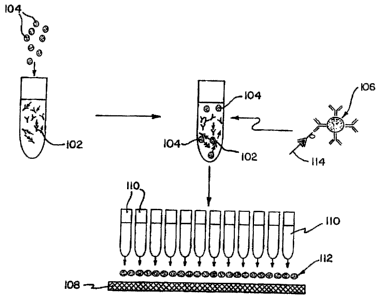
Figs. 4a and 4b show a variant in which beads in region 0 (Fig. 4a) are
split into multiple regions Fl, F2, Fn (Fig. 4b). This reversible splitting
of an
aggregate or array into n subarrays, or clusters, is accomplished, for
carboxylated
polystyrene spheres of 2 micron diameter at a concentration corresponding to
an electrode
coverage of a small fraction of a monolayer, at a frequency of 500Hz, by
raising the
applied voltage from typically 5V (pp) to 20V (pp). This fragmentation of an
array into
smaller clusters reflects the effect of a field-induced particle polarization.
The splitting
is useful to distribute particles in an array over a wider area of substrate
for presentation
to possible analytes in solution, and for subsequent scanning of the
individual clusters with
analytical instruments to make individual readings.
The three functional elements of the present invention described herein may
be also combined to yield additional fundamental operations to control the
orientation of
anisotropic objects embedded in the electroosmotic flow created by the applied
electric
field at the electrode surface. The direction of the flow, in the plane of the
substrate, is
controlled by gradients in the impedance that are shaped in the manner
described in
connection with the channeling operation. This is used to controllably align
anisotropic
objects as illustrated in Fig. lh, and may be applied to stretch out and align
biomolecules,
such as DNA.
An additional fundamental operation that complements the previous set is
that of permanently anchoring an array to the substrate. This is best
accomplished by
invoking anchoring chemistries analogous to those relying on
heterobifunctional
CA 02548805 1997-04-24
cross-linking agents invoked to anchor proteins via amide bond formation.
Molecular recognition,
for example between biotinylated particles and surface-anchored streptavidin,
provides another class
of coupling chemistries for permanent anchoring.
5 General Experimental Conditions
The functional elements, namely the electric-field induced assembly of planar
particle arrays, the spatial modulation of the interfacial impedance by means
of UV-mediated oxide
or surface-chemical patterning and finally, the control over the state of the
interfacial impedance by
10 light which are used in the present invention, have been
demonstrated in experimental studies. These
studies employed n-doped silicon wafers (resistivities in the range of 0.01
Ohm cm), capped with
either thermally grown oxide layers of several thousand Angstrom thickness, or
with thin oxide
layers, regrown after removal of the original "native" oxide in HF, under UV
illumination from a
deuterium source in the presence of oxygen to typical thicknesses between 10
and 50 Angstroms.
15 Lithographic patterning of thermally grown oxide employed
standard procedures implemented on a
bench top (rather than a clean room) to produce features in the range of
several microns.
Surfaces were carefully cleaned in adherence with industry standard RCA and
Piranha cleaning protocols. Substrates were stored in water produced by a
Millipore n4 cleaning
=
20 system prior to use. Surfaces were characterized by measuring the
contact angle exhibited by a 20
microliter droplet of water placed on the surface and viewed (from the side)
through a telescope. The
contact angle is defined as the angle subtended by the surface and the tangent
to the droplet contour
(in side view) at the point of contact with the surface. For example, a
perfectly hemispherical droplet
shape would correspond to a contact angle of 90 degrees. Surface chemical
derivatization with
mercapto-propyl-trimethoxysilane (2% in dry toluene) produced surfaces giving
typical contact
angles of 70 degrees. Oxidation of the terminal thiol functionality under UV
irradiation in the
presence of oxygen reduced the contact angle to zero in less than 10 min of
exposure to UV from the
deuterium source. Other silane reagents were used in a similar manner to
produce hydrophobic
surfaces, characterized by contact angles in excess of 110 degrees.
Simple "sandwich" electrochemical cells were constructed by employing kapton
film as a spacer between Si/SiOx and conductive indium tin oxide (ITO),
deposited
CA 02548805 1997-04-24
21
on a thin glass substrate. Contacts to platinum leads were made with silver
epoxy directly.
to the top of the ITO electrode and to the (oxide-stripped) backside of the Si
electrode.
In this two-electrode configuration, AC fields were produced by a function
generator, with
applied voltages ranging up to 20V and frequencies varying from DC to 1 MHz,
high
frequencies favoring the formation of particle chains connecting the
electrodes. Currents
were monitored with a potentiostat and displayed on an oscilloscope. For
convenience,
epi-fluorescence as well as reflection differential interference contrast
microscopy
employed laser illumination. Light-induced modulations in EIS impedance were
also
produced with a simple 100W microscope illuminator as well as with a 3mW laser
diode
emitting light at 650-680 nm.
Colloidal beads, both anionic and cationic as well as nominally neutral, with
a diameter in the range from several hundred Angstroms to 20 microns, stored
in a NaN2
solution, were employed.
Close attention was paid to colloidal stability to avoid non-specific
interactions between particles and between particles and the electrode
surface. Bacterial
contamination of colloidal suspensions was scrupulously avoided.
Typical operating conditions producing, unless otherwise indicated, most
of the results described herein, were: 0.2 mM NAN (sodium azide) solutions,
containing
particles at a concentration so as to produce not more than a complete
monolayer of
particles when deposited on the electrode; applied DC potentials in the range
of 1-4V, and
AC potentials in the range of 1-10V (peak-to-peak) and 500Hz - 10kHz, with an
electrode
gap of 50 microns; anionic (carboxylated polystyrene) beads of 2 micron
diameter, as well
as (nominally neutral) polystyrene beads of 2-20 micron diameter.
The method and apparatus of the present invention may be used in several
different areas, examples of which are discussed in detail. Each example
includes
background information followed by the application of the present invention to
that
particular application.
Example I - Fabrication of Surfaces and Coatings with Designed Properties
The present invention may be used to fabricate planar surfaces and coatings
with designed properties. Specifically, the functional elements of the present
invention
enable the formation of arrays composed of particles of a wide range of sizes
(approximately 100 Angstrom to 10 microns) and chemical composition or surface
CA 02548805 1997-04-24
22
functionality in response to AC or DC electric fields. These arrays may be
placed and.
delineated in designated areas of the substrate, and the interparticle spacing
and internal
state of order within the array may be controlled by adjusting the applied
field prior to
anchoring the array to the substrate. The newly formed surfaces display pre-
designed
mechanical, optical and chemical characteristics, and they may be subjected to
further
modification by subsequent treatment such as chemical cross-linking.
The mechanical and/or chemical modification of surfaces and coatings
principally determines the interaction between materials in a wide range of
applications
that depend on low adhesion (e.g., the familiar "non-stick" surfaces important
in
housewares) or low friction (e.g., to reduce wear in computer hard disks),
hydrophobicity
(the tendency to repel water, e.g., of certain fabrics), catalytic activity or
specific
chemical functionality to either suppress molecular interactions with surfaces
or to
promote them. The latter area is of particular importance to the development
of reliable
and durable biosensors and bioelectronic devices. Finally, a large number of
applications
depend on surfaces of defined topography and/or chemical functionality to act
as templates
controlling the growth morphology of deposited materials or as "command
surfaces"
directing the alignment of optically active molecules in deposited thin
organic films, as
in liquid crystal display applications.
Extensive research has been devoted to the formation of surfaces by
adsorption of thin organic films of known composition from the liquid or gas
phase by
several methods. Notwithstanding their seeming simplicity and wide-spread use,
these
methods can be difficult to handle in producing reliable and reproducible
results. In
addition, molecular films are not well suited to produce surfaces displaying a
regular
topography.
An alternative approach to the problem is the modification of conductive
surfaces by electrophoretic deposition of suspended particulates. This is a
widely used
technique in industrial settings to produce paint coatings of metal parts, and
to deposit
phosphor for display screens. The active deposition process significantly
enhances the
kinetics of formation (in contrast to passive adsorption of organic films from
solution),
an important consideration in practical applications. E1ectrophoretic
deposition requires
high DC electric fields and produces layers in which particles are permanently
adsorbed
to the surface. While particles in so-deposited monolayers are usually
randomly
distributed, the formation of polycrystalline monolayers of small (150
Angstrom) gold
CA 02548805 1997-04-24
23
colloids on carbon-coated copper grids is also known. However, the use of
carbon-coated
copper grids as substrates is not desirable in most applications.
Prior art methods have been described for the formation of ordered planar
arrays of particles under certain conditions. For example, the formation of
ordered
colloidal arrays in response to AC electric fields on conductive indium tin
oxide (ITO)
electrodes is known. However, the resulting layers were composed of small
patches of
ordered arrays, randomly distributed over the surface of the otherwise bare
ITO substrate.
Arrays of monodisperse colloidal beads and globular proteins also have been
previously
fabricated by using convective flow and capillary forces. However, this latter
process has
the disadvantage of leaving deposited particle arrays immobilized and exposed
to air,
making it difficult to modify arrays by subsequent liquid phase chemistry.
The present invention provides a method of forming planar arrays with
precise control over the mechanical, optical and chemical properties of the
newly created
layer. This method has several distinct advantages over the prior art. These
result from
the combination of AC electric field-induced array formation on insulating
electrodes
(Si/Si0x) that are patterned by UV-mediated oxide regrowth. The process of the
present
invention enables the formation of ordered planar arrays from the liquid phase
(in which
particles are originally suspended) in designated positions, and in accordance
with a given
overall outline. This eliminates the above-stated disadvantages of the prior
art, i.e., dry
state, irregular or no topography, random placement within an aggregate,
immobilization
of particles and uncontrolled, random placement of ordered patches on the
substrate.
An advantage of the present invention is that arrays are maintained by the
applied electric field in a liquid environment. The process leaves the array
in a state that
may be readily disassembled, subjected to further chemical modification such
as
cross-linking, or made permanent by chemical anchoring to the substrate.
Furthermore,
the liquid environment is favorable to ensure the proper functioning of many
proteins and
protein supramolecular assemblies of which arrays may be composed. It also
facilitates
the subsequent liquid-phase deposition of additional layers of molecules (by
chemical
binding to beads or proteins in the deposited layer), the cycling of arrays
between states
of different density and internal order (including complete disassembly of the
array) in
response to electric fields and the chemical cross-linking of particles into
two-dimensionally connected layers, or gels, formed, for example, of
chemically
functionalized silica spheres. The present invention can be practiced on
insulating
CA 02548805 1997-04-24
24
electrodes such as oxide-capped silicon, to minimize Faradaic processes that
might
adversely affect chemical reactions involved in the gelation process or in
anchoring the
array to the substrate. The use of Si/SiOx electrodes also enables the control
of way
= placement by external illumination.
The formation of colloidal arrays composed of small particles in accordance
= with the present invention provides a route to the fabrication of
surfaces with relief
structure on the scale of the particle diameter. Aside from their optical
properties, such
"micro-rough" surfaces are of interest as substrates for the deposition of DNA
in such a
way as to alleviate steric constraints and thus to facilitate enzyme access.
Particles to which the invention applies include silica spheres, polymer
colloids, lipid vesicles (and related assemblies) containing membrane proteins
such as
bacteriorhodopsin (bR)' a light-driven proton pump that can be extracted in
the form of
membrane patches and disks or vesicles. Structured and functionalizecl
surfaces composed
of photoactive pigments are of interest in the context of providing elements
of planar
optical devices for the development of innovative display and memory
technology. Other
areas of potential impact of topographically structured and chemically
functionalized
surfaces are the fabrication of template surfaces for the controlled
nucleation of deposited
layer growth and command surfaces for liquid crystal alignment. The present
invention
also enables the fabrication of randomly heterogeneous composite surfaces. For
example,
the formation of arrays composed of a mixture of hydrophobic and hydrophilic
beads of
the same size creates a surface whose wetting and lubrication characteristics
may be
controlled by the composition of the deposited mixed bead array. In this way,
the location
of the individual beads is random, but the relative proportion of each type of
bead within
the array is controllable.
Example II - Assembly of Lens Arrays and Optical Diffraction Elements
The present invention can be used to fabricate lens arrays and other
surface-mounted optical elements such as diffraction gratings. The functional
elements
of the present invention enable the placement and delineation of these
elements on ITO,
facilitating integration with existing planar display technology, and on
Si/SiOx, facilitating
integration with existing silicon-based device technology.
Silica or other oxide particles, polymer latex beads or other objects of high
refractive index suspended in an aqueous solution, will refract light. Ordered
planar
=
CA 02548805 1997-04-24
arrays of beads also diffract visible light, generating a characteristic
diffraction pattern of.
sharp spots. This effect forms the basis of holographic techniques in optical
information
processing applications.
5 A. - The present invention provides for the use of arrays
of refractive
colloidal beads as light collection elements in planar array formats in
conjunction with low
light level detection and CCD imaging. CCD and related area detection schemes
will
benefit from the enhanced light collection efficiency in solid-phase
fluorescence or
luminescence binding assays.
10
This assay format relies on the detection of a fluorescence signal indicating
the binding of probes to bead-anchored targets in the vicinity of the
detector. To
maximize through-put, it is desirable to monitor simultaneously as many
binding events
as possible. It is here that array formation by the methods of the present
invention is
particularly valuable because it facilitates the placement and tight packing
of beads in the
15 target area monitored by the CCD detector, while simultaneously providing
for the
additional benefit of lensing action and the resulting increase in light
collection efficiency.
Increased collection efficiency has been demonstrated in experiments
employing individual, large (10 micron diameter) polystyrene beads as lensing
elements
to image small (1 micron diameter) fluorescent polystyrene beads. Under the
20 experimental conditions set forth above an applied voltage of 5V
(pp) at 300 Hz induced
the collection of small particles under individual large beads within a
second. This is
shown in Fig. 5, where small beads alone, e.g., 52, appear dim, whereas small
beads,
e.g., 54, gathered under a large bead 56 appear brighter and magnified. The
small beads
redisperse when the voltage is turned off.
25 B. -
The use of colloidal bead arrays as diffraction gratings and thus
as holographic elements is known. Diffraction gratings have the property of
diffracting
light over a narrow range of wavelengths so that, for given angle of incidence
and
wavelength of the illuminating light, the array will pass only a specific
wavelength (or a
narrow band of wavelengths centered on the nominal value) that is determined
by the
inter-particle spacing. Widely discussed applications of diffraction gratings
range from
simple wavelength filtering to the more demanding realization of spatial
filters and related
holographic elements that are essential in optical information processing.
The present invention provides for a rapid and well controlled process of
CA 02548805 1997-04-24
26
forming planar arrays in a state of crystalline order which will function as.
surface-mounted optical diffraction elements. In addition, the resulting
surfaces may be
designed to display topographical relief to enhance wave-length selective
reflectivity.
= These arrays may be formed in designated areas on a substrate surface. In
contrast to the
slow and cumbersome prior art method of fabricating such arrays by way of
forming
=
equilibrium crystals in aqueous solutions of low salt content, the present
invention
provides a novel approach to rapidly and reliably fabricate particle arrays at
a solid-liquid
interface. This approach relies on field-induced formation of arrays to
trigger the process,
and on UV-mediated patterning or light control to position and shape the
arrays. In
addition, the inter-particle distance, and internal state of order, and hence
the diffraction
characteristics of the array, may be fine-tuned by adjusting the applied
electric field. For
example, a field-induced, reversible order-disorder transition in the array
will alter the
diffraction pattern from one composed of sharp spots to one composed of a
diffuse ring.
The assembly of such arrays on the surface of silicon wafers, as described
herein,
provides a direct method of integration into existing microelectronic designs.
Arrays may
be locked in place by chemical coupling to the substrate surface, or by
relying on van der
Waals attraction between beads and substrate.
Example III - A Novel Mechanism for the Realization of a Particle-Based
Display
The present invention provides the elements to implement lateral particle
motion as a novel approach to the realization of a particle-based display. The
elements
of the present invention provide for the control of the lateral motion of
small particles in
the presence of a pre-formed lens array composed of large, refractive
particles.
Colloidal particulates have been previously employed in flat-panel display
technology. The operating principle of these designs is based on
electrophoretic motion
of pigments in a colored fluid confined between two planar electrodes. In the
OFF (dark)
state, pigments are suspended in the fluid, and the color of the fluid defines
the
appearance of the display in that state. To attain the ON (bright) state,
particles are
assembled near the front (transparent) electrode under the action of an
electric field. In
this latter state, incident light is reflected by the layer of particles
assembled near the
electrode, and the display appears bright. Prototype displays employing small
reflective
particles in accordance with this design are known. However, these displays
suffered
from a number of serious problems including: electrochemical degradation and
lack of
=
CA 02548805 1997-04-24
27
colloidal stability as a result of prolonged exposure to the high DC electric
fields required
to achieve acceptable switching speeds; and non-uniformities introduced by
particle
migration in response to field gradients inherent in the design of the
addressing scheme.
The present invention provides a novel mechanism for the design of a
particle-based display which takes advantage of electric field-induced array
formation as
well as controlled, field-induced lateral particle displacements. First, a
lens array
composed of colloidal beads is formed. This lens array also serves as a spacer
array to
maintain a well-defined gap between the bottom electrode and the top electrode
that may
now be placed over the (pre-fonned) array. This facilitates fabrication of
uniform flat
panel displays with a narrow gap that is determined by the particle diameter.
Next, small colloidal particles are added to the electrolyte solution in the
gap. These may be fluorescent, or may be reflecting incident white light.
Under the
action of an AC electric field of appropriate frequency, these small particles
can be moved
laterally to assemble preferentially within the footprint of a larger bead.
When viewed
through a larger bead, small fluorescent beads assembled under a large bead
appear bright
as a result of the increased light collection efficiency provided by the
lensing action of the
large bead; this is the ON state (Fig. 5). When moved outside the footprint of
the larger
bead, particles appear dim, and may be made entirely invisible by appropriate
masking;
this is the OFF state. The requisite lateral particle motion may be induced by
a change
in the applied voltage or a change in light intensity. Each large or lensing
bead introduces
a lateral nonuniformity in the current distribution within the electrolyte
because the current
is perturbed by the presence of each lensing bead.
In contrast to the prior art displays, the present invention employs AC, not
DC fields, and insulating (rather than conductive) electrodes, thereby
minimizing
electrochemical degradation. The lateral non-uniformity introduced by the lens
array is
desirable because it introduces lateral gradients in the current distribution
within the
display cell. These gradients mediate the lateral motion of small beads over
short
characteristic distances set by the diameter of the large lensing beads, to
effect a switching
between ON and OFF states. Thus, the present invention readily accommodates
existing
technology for active matrix addressing.
Example IV - Layout-Preserving Transfer of Bead Suspensions from Microtiter
Plate to
Planar Cell
CA 02548805 1997-04-24
28
The present invention provides a method to transfer suspensions of beads.
or biomolecules to the electrode surface in such a way as to preserve the
spatial encoding
in the original arrangement of reservoirs, most commonly the conventional 8x12
= arrangement of wells in a microtiter plate. Such a fluid transfer scheme
is of significant
practical importance given that compound libraries are commonly handled and
shipped in
8x12 wells.
The present invention utilizes chemical patterning to define individual
compartments for each of MxN sets of beads and confine them accordingly. In
the
present instance, patterning is achieved by UV-mediated photochemical
oxidation of a
monolayer of thiol-terminated alkylsilane that is chemisorbed to the Si/SiOx
substrate.
Partial oxidation of thiol moities produces sulfonate moities and renders the
exposed
surface charged and hydrophilic. The hydrophilic portions of the surface, in
the form of
a grid of squares or circles, will serve as holding areas.
In accordance with the present invention, the first function of
surface-chemical patterning into hydrophilic sections surrounded by
hydrophobic portions
is to ensure that droplets, dispensed from different wells, will not fuse once
they are in
contact with the substrate. Consequently, respective bead suspensions will
remain
spatially isolated and preserve the lay-out of the original MxN well plate.
The second
role of the surface chemical patterning of the present invention is to impose
a surface
charge distribution, in the form of the MxN grid pattern, which ensures that
individual
bead arrays will remain confined to their respective holding areas even as the
liquid phase
becomes contiguous.
The transfer procedure involves the steps illustrated in Figs. 6a-c. First,
as shown in sideview in Fig. 6a, the MxN plate of wells 62 is registered with
the pattern
64 on the planar substrate surface. Well bottoms 62, are pierced to allow for
the
formation of pendant drops of suspension or, preferably, the process is
facilitated by a
fixture (not shown) providing MxN effective funnels to match the geometric
dimensions
of the Midst plate on the top and reduce the size of the dispensing end. Such
a dispensing
fixture will also ensure the precise control of droplet volumes, adjusted so
as to slightly
overfill the target holding area on the patterned substrate surface. The set
of MxN drops
is then deposited by bringing them in contact with the hydrophilic holding
areas of the
pre-patterned substrate and relying on capillary action.
Next, the plate is retracted, and the top electrode is carefully lowered to
CA 02548805 1997-04-24
29
form the electrochemical cell, first making contact as shown in Fig. 6b, with
individual..
liquid-filled holding areas on the substrate to which suspensions are
confined. Overfilling
ensures that contact is made with individual suspensions. The electric field
is now turned
on to induce array formation in the MxN holding areas and to ensure the
preservation of
the overall configuration of the MxN sets of beads while the gap is closed
further (or
filled with additional buffer) to eventually fuse individual droplets of
suspension into a
contiguous liquid phase as shown in Fig. 6c. In the fully assembled cell of
Fig. 6c, while
the droplets are fused together, the beads from each droplet are maintained in
and isolated
in their respective positions, reflecting the original MEN arrangement of
wells. The
present invention thus provides for the operations required in this
implementation of a
layout-preserving transfer procedure to load planar electrochemical cells.
Example V - Preparation of Heterogeneous Panels of Particles
The present invention provides a method to produce a heterogeneous panel
of beads and potentially of biomolecules for presentation to analytes in an
adjacent liquid.
A heterogeneous panel contains particles or biomolecules which differ in the
nature of the
chemical or biochemical binding sites they offer to analytes in solution. In
the event of
binding, the analyte is identified by the coordinates of the bead, or cluster
of beads,
scoring positive. The present method relies on the functional elements of the
invention
to assemble a planar array of a multi-component mixture of beads which carry
chemical
labels in the form of tag molecules and may be so identified subsequent to
performing the
assay.
Diagnostic assays are frequently implemented in a planar format of a
heterogeneous panel, composed of simple ligands, proteins and other
biomolecular targets.
For example, in a diagnostic test kit, a heterogeneous panel facilitates the
rapid testing of
a given analyte, added in solution, against an entire set of targets.
Heterogeneous panels
of proteins are of great current interest in connection with the emerging
field of proteome
research. The objective of this research is to identify, by scanning the panel
with
sensitive analytical techniques such as mass spectrometry, each protein in a
multi-component mixture extracted from a cell and separated by two-dimensional
gel
electrophoresis. Ideally, the location of each spot uniquely corresponds to
one particular
protein. This analysis would permit, for example, the direct monitoring of
gene
expression levels in a cell during a particular point in its cycle or at a
given stage during
CA 02548805 1997-04-24
embryonic development.
The fabrication of an array of heterogeneous targets is central to recently
proposed
5 strategies of drug screening and DNA mutation analysis in a planar
format. The placement of ligands
in a specific configuration on the surface of a planar substrate serves to
maintain a key to the identity
of any one in a large set of targets presented simultaneously to an analyte in
solution for binding or
hybridization. In an assay relying on fluorescence, binding to a specific
target will create bright spots
on the substrate whose spatial coordinates directly indicate the identity of
the target.
Three principal strategies have been previously employed to fabricate
heterogeneous
panels. First, protein panels may be created by two-dimensional gel
electrophoresis, relying on a DC
electric field to separate proteins first by charge and then by size (or
molecular weight). Even after
many years of refinement, this technique yields results of poor
reproducibility which are generally
attributed to the poorly defined properties of the gel matrix.
Second, individual droplets, drawn from a set of reservoirs containing
solutions of
the different targets, may be dispensed either by hand or by employing one of
several methods of
automated dispensing (or "printing"; see e.g., Schena et al., Science 270, 467-
470 (1995). Printing
has been applied to create panels of oligonucleotides intended for screening
assays based on
hybridization. Printing leaves a dried sample and may thus not be suitable for
proteins that would
denature under such conditions. In addition, the attendant fluid handling
problems inherent in
maintaining, and drawing samples from a large number of reservoirs are
formidable.
Third, target ligands may be created by invoking a variant of solid phase
synthesis
based on a combinatorial strategy of photochemically activated elongation
reactions. This approach
has been limited by very formidable technical problems in the chemical
synthesis of even the
simplest, linear oligomers. The synthesis of non-linear compounds in this
planar geometry is
extremely difficult.
The present invention of forming heterogeneous panels requires the chemical
attachment of target ligands to beads. Ligands may be coupled to beads "off-
line" by a variety of
well established coupling reactions. For present purposes, the bead identity
must be chemically
encoded so it may be determined as needed. Several methods of encoding, or
binary encoding, of
beads are available. For example, short
CA 02548805 1997-04-24
31
oligonucleotides may serve the purpose of identifying a bead via their
sequence which may
be determined by microscale sequencing techniques. Alternatively, chemically
inert
molecular tags may be employed that are readily identified by standard
analytical
techniques.
In contrast to all prior art methods, the present invention provides a novel
method to create heterogeneous panels by in-situ, reversible formation of a
planar array
of "encoded" beads in solution adjacent to an electrode. The way may be random
with
respect to chemical identity but is ordered with respect to spatial position.
This procedure
offers several advantages. First, it is reversible so that the panel may be
disassembled
following the binding assay to discard beads scoring negative. Positive beads
may be
subjected to additional analysis without the need for intermediate steps of
sample retrieval,
purification or transfer between containers. Second, the panel is formed when
needed,
that is, either prior to performing the actual binding assay, or subsequent to
performing
the assay on the surface of individual beads in suspension. The latter mode
minimizes
potential adverse effects that can arise when probes bind to planar target
surfaces with a
high concentration of target sites. Third, to accommodate scanning probe
analysis of
individual beads, interparticle distances within the array may be adjusted by
field-induced
polarization or by the addition of inert spacer particles that differ in size
from the encoded
beads. Fig. 7 shows the use of small spacer beads 72 for separating encoded
beads 74.
As shown, the spacing of beads 74 is greater than the spacing of comparable
beads in Fig.
4b. Finally, UV-mediated oxide regrowth, as provided by the present invention,
readily
facilitates the embedding of a grid pattern of selected dimension into the
substrate to
ensure the formation of small, layout-preserving subarrays in the low-
impedance fields of
the grid.
To create the panel, a multi-component mixture of beads carrying, for
example, compounds produced by bead-based combinatorial chemistry, is placed
between
electrodes. Each type of bead may be present in multiple copies. Arrays are
formed in
response to an external field in a designated area of the electrode surface.
This novel
approach of in-situ assembly of panels relies on beads that carry a unique
chemical label,
or code, to permit their identification subsequent to the completion of a
binding assay.
This invention facilitates on-line tagging of beads by way of a photochemical
bead-
coloring method. Selected beads in an array are individually illuminated by a
focused
light source to trigger a coloring reaction on the bead surface or in the bead
interior to
CA 02548805 1997-04-24
32
indicate a positive assay score. Beads so marked can be subsequently separated
from
unmarked beads by a light-activated sorting method described herein. Numerous
UV-
activated reactions are available to implement this bead-coloring method.
= The present invention provides for several methods of discarding beads
with
negative scores, typically the vast majority, while retaining those with
positive scores.
This method take advantage of the fact that, in contrast to all prior art
methods, the array
represents a temporary configuration of particles that is maintained by the
applied electric
field and may be rearranged or disassembled at will. This capability, along
with the fact
that biomolecules are never exposed to air (as in the prior art method of
printing)
facilitates the in-situ concatenation of analytical procedures that require
the heterogeneous
panel in conjunction with subsequent, "downstream" analysis.
First, if positive beads are clustered in a subsection of the array, the
light-controlled array splitting operation of the present invention may be
invoked to dissect
the array so as to discard negative portions of the array (or recycle them for
subsequent
use).
Second, if positive and negative beads are randomly interspersed, a
fluorescence-activated sorting method, implemented on the basis of the present
invention
in a planar format, as described herein, may be invoked. In the case of
fluorescence-
activated sorting, positive and negative beads may be identified as bright and
dark objects,
respectively. In the special case that only a few positive beads stand out,
these may be
removed from the array by locking onto them with optical tweezers, a tool to
trap and/or
manipulate individual refractive particles under illumination, and
disassembling the array
by removing the field, or subjecting the entire array to lateral displacement
by the
fundamental operations of the present invention.
The typical task in screening a large set of compounds is one of looking for
a very small number of positive events in a vast number of tests. The set of
discarded
beads will typically involve the majority at each stage in the assay. The
procedure of the
present invention therefore minimizes the effort invested in negative events,
such as the
challenging in-situ synthesis of target ligands irrespective of whether or not
they will
prove to be of interest by binding a probe offered in solution.
The method of forming a heterogeneous panel according to the present
invention contains beads of each type in generally random assembly. The
creation of a
heterogeneous panel with each position in the panel containing a cluster of
beads of the
same type, that is, beads originating in the same reservoir (Fig. 6a), may be
desirable so
CA 02548805 1997-04-24
33
as to ensure a sufficiently large number of positive events to facilitate
detection. A
practical solution follows from the application of the layout-preserving
fluidic transfer
scheme described herein. In this procedure, beads from an MxN well plate are
transferred layout-preservingly onto a chemically patterned substrate in such
a way as to
preserve the spatial encoding of bead identities.
Example VI - Binding and Functional Assays in Planar Bead Array Format
The present invention can be used to implement mixed-phase binding assays
as well as certain functional assays in a planar array format. Several
combinations are
possible reflecting the presence of probe or target in solution, on the
surface of colloidal
beads, or on the electrode surface. The methods of the present invention
facilitate the
formation of a planar array to present targets to probes in solution prior to
performing the
binding assay ("preformed" array; Fig. 8). Alternatively, a planar array of
beads may be
formed in front of a detector surface subsequent to performing the binding
assay in
suspension (wpostformed" array; Fig. 8). The present invention also provides
the methods
to implement functional assays by enabling the assembly of certain cell types
adjacent to
a planar detector or sensor surface to monitor the effects of exposure of the
cells to small
molecule drugs in solution.
Binding assays, particularly those involving proteins such as enzymes and
antibodies, represent a principal tool of medical diagnostics. They are based
on the
specific biochemical interaction between a probe, such as a small molecule,
and a target,
such as a protein. Assays facilitate the rapid detection of small quantities
of an analyte
in solution with high molecular specificity. Many procedures have been
designed to
produce signals to indicate binding, either yielding a qualitative answer
(binding or no
binding) or quantitative results in the form of binding or association
constants. For
example, when an enzyme binds an analyte, the resulting catalytic reaction may
be used
to generate a simple color change to indicate binding, or it may be coupled to
other
processes to produce chemical or electrical signals from which binding
constants are
determined. Monoclonal antibodies, raised from a single common precursor, may
be
prepared to recognize virtually any given target, and immunoassays, based on
antibody-antigen recognition and binding, have developed into an important
diagnostic
tool. As with enzyme binding, antibody binding of an antigenic analyte may be
detected
by a variety of techniques including the classic method of enzyme-linked
immunoassays
CA 02548805 1997-04-24
34
(ELISA) in which the reaction of an antibody-coupled enzyme is exploited as an
indicator. A
common and conceptually simple scheme ensures the detection of antibody
binding to a target
analyte by supplying a fluorescently labeled second antibody that recognizes
the first (or primary)
antibody.
Binding assays involving soluble globular proteins are often performed in
solution to
ensure unbiased interactions between protein and target. Such liquid phase
assays, especially when
performed at low concentrations of target or probe, minimize potential
difficulties that may arise
when either target or probe are present in abundance or in close proximity. By
the same token; the
kinetics tend to be slow. Cooperative effects, such as crowding, arising from
the close proximity of
probes must be carefully controlled when either probe or target is chemically
anchored to a solid
substrate.
Nonetheless, this latter solid phase format of binding assays is also very
commonly
employed whenever the situation demands it. For example, the presence of a
protein on the surface
of a cell may be exploited in "panning" for the cells that express this
protein in the presence of many
other cells in a culture that do not: desired cells attach themselves to the
surface of a container that is
pre-coated with a layer of a secondary antibody directed against a primary
antibody decorating the
desired cell-surface protein. Similarly, certain phages may be genetically
manipulated to display
proteins on their surface, and these may be identified by a binding assay
involving a small molecule
probe such as an antigen if the protein displayed is an antibody (Watson et
al., "Recombinant
DNA", 2nd Edition (Scientific American Books, W.H. Freeman and Co., New York,
NY, 1983)).
In addition, planar geometry accommodates a variety of optical and electrical
detection schemes
implemented in transducers and sensors.
A combination of liquid phase and solid phase assay may be developed by using
beads that are decorated with either probe or target, as in procedures that
employ decorated magnetic
beads for sample preparation or purification by isolating binding from non-
binding molecules in a
given multi-component mixture. Recent examples of the use of these beads
include the purification
of templates for DNA sequencing applications or the extraction of mRNAs from
(lysed) cells by
hybridization to beads that are decorated with poly-adenine (polyA) residues.
Functional assays involving suitable types of cells are employed to monitor
extracellular effects of small molecule drugs on cell metabolism. Cells are
placed in the
CA 02548805 1997-04-24
immediate vicinity of a planar sensor to maximize the local concentration of
agents.
released by the cell or to monitor the local pH.
The present invention provides the means to implement mixed phase binding
assays in a planar geometry with a degree of flexibility and control that is
not available
5 by prior art methods. Thus, it offers the flexibility of forming, in-
situ, reversibly and
under external spatial control, either a planar panel of target sites for
binding of analyte
present in an adjacent liquid phase, or a planar array of probe-target
complexes subsequent
to performing a binding assay in solution. Binding may take place at the
surface of
individual beads suspended in solution, at the surface of beads pre-assembled
into ways
10 adjacent to the electrode surface, or at the electrode surface
itself. Either the target or
probe molecule must be located on a bead to allow for a bead-based assay
according to
the present invention. As shown in Fig. 8, if the probe molecule P is located
on a bead,
then the target molecule T may be either in solution, on a bead or on the
electrode
surface. The converse is also true.
15 For example, the methods of the present invention may be used to
implement panning, practiced to clone cell surface receptors, in a far more
expeditious
and controlled manner than is possible by the prior art method. Given a
substrate that has
been coated with a layer of antibody directed against the sought-after cell
surface protein,
the present inventiontacilitates the rapid assembly of a planar array of cells
or decorated
20 beads in proximity to the layer of antibodies and the subsequent
disassembly of the array
to leave behind only those cells or beads capable of forming a complex with
the
surface-bound antibody.
A further example of interest in this category pertains to phage displays.
This technique may be employed to present a layer of protein targets to bead-
anchored
25
probes. Bead arrays may now be employed to identify a protein of interest.
That is,
_
beads are decorated with small molecule probes and an array is formed adjacent
to the
phage display. Binding will result in a probe-target complex that retains
beads while
others are removed when the electric field is turned off, or when light-
control is applied
to remove beads from the phage display. If beads are encoded, many binding
tests may
30 be carried out in parallel because retained beads may be
individually identified subsequent
to binding.
The methods of the present invention readily facilitate competitive binding
assays. For example, subsequent to binding of a fluorescent probe to a target-
decorated
'
CA 02548805 1997-04-24
36
bead in solution and the formation of a planar bead array adjacent to the
electrode, .
fluorescent areas within the array indicate the position of positive targets,
and these may
be further probed by subjecting them to competitive binding. That is, while
monitoring
the fluorescence of a selected section of the planar array, an inhibitor (for
enzyme assays)
or other antagonist (of known binding constant) is added to the
electrochemical cell, and
the decrease in fluorescence originating from the region of interest is
measured as a
function of antagonist concentration to determine a binding constant for the
original probe.
This is an example of a concatenation of analytical steps that is enabled by
the methods
of the present invention.
The fact that a probe-target complex is fixed to a colloidal bead, as in the
methods of the present invention, conveys practical advantages because this
facilitates
separation of positive from negative events. Particularly when solid phase
assays are
performed on a planar substrate, an additional advantage of planar bead arrays
is the
enhancement of light collection efficiency provided by the beads, as discussed
herein.
If desired, beads may serve strictly as delivery vehicles for small molecule
probes. That is, an array of probe-decorated beads is formed adjacent to a
target-
decorated surface in accordance with the methods of the present invention. UV-
activated
cleavage of the probe from the bead support will ensure that the probe is
released in close
proximity to the target layer, thereby enhancing speed and efficiency of the
assay. The
identity of the particular probe interacting with the target may be
ascertained from the
positional location of the bead delivering the probe.
The methods of the preset* invention apply not only to colloidal beads of
a wide variety (that need no special preparative procedures to make them
magnetic, for
example), but also to lipid vesicles and cells that are decorated with, or
contain embedded
in their outer wall, either probe or target. The methods of the present
invention may
therefore be applied not only to bead-anchored soluble proteins but
potentially to integral
membrane receptors or to cell surface receptors.
In particular, the rapid assembly of cells in a designated area of the
substrate surface facilitates the implementation of highly parallel cell-based
functional
assays. The present invention makes it possible to expose cells to small
molecule drug
candidates in solution and rapidly assemble them in the vicinity of a sensor
embedded in
the electrode surface, or to expose pm-assembled cells to such agents that are
released into
the adjacent liquid phase. In the simplest case, all cells will be of the same
type, and
- '
CA 02548805 1997-04-24
37
agents will be administered sequentially. Even in this sequential version,
electrokinetic
mixing will enhance through-put. However, as described herein, the methods of
the present
invention also enable the parallel version of binding assays and thus of
functional assays in a
planar format by encoding the identity of different cells by a "Layout-
Preserving Transfer"
process from an 8x12 well plate, as discussed herein, and to isolate cells
scoring positive by
providing feed-back from a spatially resolved imaging or sensing process to
target a specific
location in the array of cells.
Example VII- Separation and Sorting of Beads and Particles
The present invention can be used to implement several procedures for the
separation and sorting of colloidal particles and biomolecules in a planar
geometry.
Specifically, these include techniques of lateral separation of beads in
mixtures. Individual
beads may be removed from an array formed in response to an electric field by
the
application of optical tweezers.
The separation of components in a given mixture of chemical compounds is a
fundamental task of analytical chemistry. Similarly, biochemical analysis
frequently calls for
the separation of biomolecules, beads or cells according to size and/or
surface charge by
electrophoretic techniques, while the sorting (most commonly into just two sub-
classes) of
suspended cells or whole chromosomes according to optical properties such as
fluorescence
emission is usually performed using field-flow fractionation including flow
cytometry and
fluorescence-activated cell sorting.
In a planar geometry, bead mixtures undergoing diffusion have been
previously separated according to mobility by application of an AC electric
field in
conjunction with lithographic patterning of the electrode surface designed to
promote
directional drift. Essentially, the AC or pulsing electric field is used to
move small beads in a
particular direction over a period of time. Capillary electrophoresis has been
implemented in
a planar geometry, see e.g., B.B. Haab and R.A. Mathies, Anal. Chem 67, 3253-
3260 (1995).
The methods of the present invention may be applied in several ways to
implement the task of separation, sorting or isolation in a planar geometry.
In contrast to the
prior art approaches, the present invention provides a significant degree of
flexibility in
selecting from among several available procedures, the one best suited to the
particular task
at hand. In some cases, more than one separation technique may be
CA 02548805 1997-04-24
38
applied, and this provides the basis for the implementation of two-dimensional
separation. .
That is, beads may be separated according to two different physical-chemical
characteristics. For example, beads may first be separated by size and
subsequently, by
raising the applied frequency to induce chain formation, by polarizability.
This flexibility
offers particular advantages in the context of integrating analytical
functionalities in a
planar geometry. Several techniques will now be described.
i) The present invention may be used to implement "sieving"
in lateral,
electric field-induced flow on surfaces patterned by UV-mediated oxide
regrowth to sort
beads in a mixture by size. The fundamental operations of the invention are
invoked to
set up directed lateral particle motion along conduits laid out by UV-mediated
oxide
regrowth. Conduits are designed to contain successively narrower constrictions
through
which particles must pass. Successively finer stages allow only successively
smaller
particles to pass in this "sieving" mechanism (Fig. 9a). As shown in Fig. 9a,
the primary
particle flow is in the direction left to right, while a transverse flow is
established in the
top to bottom direction utilizing an oxide profile as shown. Additionally,
rows of barriers
92 made from thick oxide are positioned along the conduit with the spacing
between the
barriers in each row decreasing in the transverse direction. As the particles
move along
the conduit, the rows of barriers act to separate out smaller particles in the
transverse
direction. In contrast to previous methods based on electrophoretic
separation, large DC
electric fields, and the attendant potential problem of electrolysis and
interference from
electroosmotic flow in a direction opposite to the field-directed particle
transport, the
present invention uses AC electric fields and lateral gradients in interfacial
impedance to
produce transport. The present method has the advantage of avoiding
electrolysis and it
takes explicit advantage of electroosmotic flow to produce and control
particle transport.
In addition, the use of Si/SiOx electrodes enables the use of the light-
control
component of the present invention to modify lateral transport of beads in
real time. For
example, external illumination may be employed to locally neutralize the
lateral impedance
gradient induced by UV-mediated oxide regrowth. Particles in these neutral
"zones"
would no longer experience any net force and come to rest. This principle may
be used
as a basis for the implementation of a scheme to locally concentrate particles
into sharp
bands and thereby to improve resolution in subsequent separation.
The present invention may be used to implement "zone refining",
a process of excluding minority components of a mixture by size or shape from
a growing
CA 02548805 1997-04-24
39
crystalline array of majority component. This process explicitly depends on
the .
capabilities of the present invention to induce directional crystallization.
The process of zone refining is employed with great success in producing
large single crystals of silicon of very high purity by excluding impurities
from the host
lattice. The concept is familiar from the standard chemical procedure of
purification by
recrystalli72tion in which atoms or molecules that are sufficiently different
in size, shape
or charge from the host species so as not to fit into the forming host crystal
lattice as a
substitutional impurity, are ejected into solution.
By enabling the growth of planar arrays, in a given direction and at a
controlled rate, the present invention facilitates the implementation of an
analogous zone
refining process for planar arrays. The most basic geometry is the linear
geometry. A
multi-component mixture of beads of different sizes and/or shapes is first
captured in a
rectangular holding area on the surface, laid out by UV-patterning. Next,
crystallization
is initiated at one end of the holding area by illumination and allowed to
slowly advance
across the entire holding area in response to an advancing pattern of
illumination. In
general, differences of approximately 10% in bead radius trigger ejection.
The present invention may be used to implement fractionation in a
transverse flow in a manner that separates particles according to mobility.
Field-flow fractionation refers to an entire class of techniques that are in
wide use for the separation of molecules or suspended particles. The principle
is to
separate particles subjected to fluid flow in a field acting transverse to the
flow. A
category of such techniques is subsumed under the heading of electric-field
flow
fractionation of which free-flow electrophoresis is a pertinent example
because it is
compatible with a planar geometry. Free-flow electrophoresis employs the
continuous
flow of a replenished buffer between two narrowly spaced plates in the
presence of a DC
electric field that is applied in the plane of the bounding plates transverse
to the direction
of fluid flow. As they traverse the electric field, charged particles are
deflected in
proportion to their electrophoretic mobility and collected in separate outlets
for subsequent
analysis. In contrast to conventional electrophoresis, free-flow
electrophoresis is a
continuous process with high throughput and it requires no supporting medium
such as a
gel.
The present invention enables the implementation of field-flow fractionation
in a planar geometry. As previously discussed herein, impedance gradients
imposed by
CA 02548805 1997-04-24
UV-oxide profiling serve to mediate particle motion along the electrode
surface in
response to the external electric field. In a cell with a narrow gap, the
resulting
electrokinetic flow has a "plug" profile and this has the advantage of
exposing all particles
to identical values of the flow velocity field, thereby minimizing band
distortions
5 introduced by the parabolic velocity profile of the laminar flow typically
employed in
free-flow electrophoresis.
A second flow field, transverse to the primary flow direction, may be
employed to mediate particle separation. This deflecting flow may be generated
in
response to a second impedance gradient. A convenient method of imposing this
second
10 gradient is to take advantage of UV-oxide patterning to design
appropriate flow fields.
Both longitudinal and transverse flow would be recirculating and thus permit
continuous
operation even in a closed cell, in contrast to any related prior art
technique.
Additional flexibility is afforded by invoking the light-control component
of the present invention to illuminate the substrate with a stationary pattern
whose
15 intensity profile in the direction transverse to the primary fluid flow
is designed to induce
the desired impedance gradient and hence produce a transverse fluid flow.
(Fig. 9b).
This has the significant advantage of permitting selective activation of the
transverse flow
in response to the detection of a fluorescent bead crossing a monitoring
window upstream.
Non-fluorescent beads would not activate the transverse flow and would not be
deflected.
20 This procedure represents a planar analog of flow cytometry, or
fluorescence-activated cell
sorting.
iv) The invention may be used to induce the formation of particle chains
in the direction normal to the plane of the electrode. The chains represent
conduits for
current transport between the electrodes and their formation may reflect a
field-induced
25 polarization. Chains are much less mobile in transverse flow than are
individual particles
so that this effect may be used to separate particles according to the surface
properties that
contribute to the net polarization. The effect of reversible chain formation
has been
demonstrated under the experimental conditions stated herein. For example, the
reversible
formation of chains occurs, for carboxylated polystyrene beads of 1 micron
diameter, at
30 a voltage of 15 V (pp) at frequencies in excess of 1MRz.
v) The invention may be used to isolate individual beads from a planar
array.
Fluorescence binding assays in a planar array format, as described herein,
CA 02548805 1997-04-24
41
may produce singular, bright beads within a large array, indicating
particularly strong binding. To
isolate and retrieve the corresponding beads, optical tweezers in the form of
a sharply focused laser
spot, may be employed to lock onto an individual bead of interest. The light-
control component of
the present invention may be used in conjunction with the optical tweezers to
retrieve such an
individual bead by moving the array relative to the bead, or vice versa, or by
disassembling the
array and retaining only the marked bead. This is a rather unique capability
that will be particularly
useful in the context of isolating beads in certain binding assays.
Commercial instrumentation is available to position optical tweezers in the
field of
a microscope. Larger scale motion is facilitated by translocating the array in-
situ or simply by
moving the external sample fixture. This process lends itself to automation in
conjunction with the
use of peak-finding image analysis software and feedback control.
vi) The invention may be used to implement a light-induced array sectioning
("shearing") operation to separate fluorescent, or otherwise delineated
portions of an array from.
the remainder. This operation makes it possible to segment a given array and
to isolate the
corresponding beads for downstream analysis.
The basis for the implementation of this array segmentation is the light-
control
component of the present invention, in the mode of driving particles from an
area of a Si/SiOx
interface that is illuminated with high intensity. It is emphasized here that
this effect is completely
unrelated to the light-induced force on beads that underlies the action of
optical tweezers. The
present effect which operates on large sets of particles, was demonstrated
under the experimental
conditions stated herein using a 100W illuminator on a Zeiss UEM1/4 microscope
operated in epi-
illumination. A simple implementation is to superimpose, on the uniform
illumination pattern
applied to the entire array, a line-focussed beam that is positioned by
manipulation of beam
steering elements external to the microscope. Beads are driven out of the
illuminated linear
portion. Other implementations take advantage of two separately controlled
beams that are
partially superimposed. The linear sectioning can be repeated in different
relative orientations of
shear and array.
Example VIII- Screening for Drug Discovery in Planar Geometry
The functional elements of the present invention may be combined to implement
procedures for handling and screening of compound and combinatorial libraries
CA 02548805 1997-04-24
42
in a pbna r format. The principal requisite elements of this task are: sample
and reagent .
delivery from the set of original sample reservoirs, commonly in a format of
8x12 wells
in a microtiter plate, into a planar cell; fabrication of planar arrays of
targets or of
= probe-target complexes adjacent to the planar electrode surface prior to
or subsequent to
performing a binding assay; evaluation of the binding assay by imaging the
spatial
distribution of marker fluorescence or radioactivity, optionally followed by
quantitative
phannacokinetic measurements of affinity or binding constants; isolation of
beads scoring
positive, and removal from further processing of other beads; and collection
of specific
beads for additional downstream analysis. The present invention relates to all
of these
elements, and the fundamental operations of the invention provide the means to
concatenate these procedures in a planar format.
A central issue in the implementation of cost-effective strategies for modern
therapeutic drug discovery is the design and implementation of screening
assays in a
manner facilitating high throughput while providing pharmacokinetic data as a
basis to
select promising drug leads from a typically vast library of compounds. That
is,
molecular specificity for the target, characterized by a binding constant, is
an important
factor in the evaluation of a new compound as a potential therapeutic agent.
Common
targets include enzymes and receptors as well as nucleic acid ligands
displaying
characteristic secondary structure.
The emerging paradigm for lead discovery in pharmaceutical and related
industries such as agricultural biotechnology, is the assembly of novel
synthetic compound
libraries by a broad variety of new methods of solid state "combinatorial"
synthesis.
Combinatorial chemistry refers to a category of strategies for the parallel
synthesis and
testing of multiple compounds or compound mixtures in solution or on solid
supports.
For example, a combinatorial synthesis of a linear oligopeptide containing n
amino acids
would simultaneously create all compounds representing the possible sequence
permutations of n amino acids. The most commonly employed implementation of
combinatorial synthesis relies on colloidal bead supports to encode reaction
steps and thus
the identity of each compound. Beads preferred in current practice tend to be
large (up
to 500 microns in diameter) and porous to maximize their compound storage
capacity, and
they must be encoded to preserve the identity of the compound they carry.
Several methods of encoding, or binary encoding, of beads are available.
Two examples are as follows. First, beads may be labeled with short
oligonucleotides
=
CA 02548805 1997-04-24
43
such as the 17-mers typically employed in hybridization experiments. The
sequence of .
such short probes may be determined by microscale sequencing techniques such
as direct
Maxam-Gilbert sequencing or mass spectrometry. This encoding scheme is
suitable when
the task calls for screening of libraries of nucleic acid ligands or
oligopeptides. Second,
members of a combinatorial library may be associated with chemically inert
molecular
tags. In contrast to the previous case, these tag molecules are not
sequentially linked.
Instead, the sequence of reaction steps is encoded by the formal assignment of
a binary
code to individual tag molecules and their mixtures that are attached to the
bead in each
successive reaction step. The tags are readily identified by standard
analytical techniques
such as gas chromatography. This general encoding strategy is currently
employed in the
synthesis of combinatorial libraries on colloidal beads.
Commercial compound libraries are large, given that even for the
aforementioned 17-mer, the number of sequence permutations is 4'17, or
approximately
10^10. However, the high specificity of typical biological substrate-target
interactions
implies that the vast majority of compounds in the collection will be inactive
for any one
particular target. The task of screening is to select from this large set the
few potential
lead compounds displaying activity in binding or in functional assays. The
principal drug
discovery strategy widely applied to natural compound libraries in the
pharmaceutical
industry is to select individual compounds from the library at random and
subject them
to a series of tests. Systematic screening procedures are thus required to
implement the
rapid screening and scoring of an entire library of synthetic compounds, in
practice often
containing on the order of 10'1 items.
In current practice, compounds are first cleaved and eluted from their solid
supports and are stored in microtiter plates. Further sample handling in the
course of
screening relies primarily on robotic pipetting and transfer between different
containers,
typically wells in microtiter plates. While robotic workstations represent a
step in the
direction of automating the process, they rely on the traditional format of
microtiter plates
containing 8x12 wells and sample handling by pipetting and thus represent
merely an
incremental operational improvement. A significant additional consideration is
the need
to conserve reagent and sample by reducing the spatial scale of the analytical
procedures.
The present invention provides a set of operations to realize integrated
sample handling and screening procedures for bead-based compound libraries in
a planar
format. This will significantly reduce time and cost due to reagent and sample
volumes.
=
CA 02548805 1997-04-24
44
The principal advantage of the methods of the present invention is that they
provide a
large set of fundamental operations to manipulate sets of beads in a planar
format,
permitting the handling of beads between stations in a multi-step analytical
procedure.
= In particular, as previously described herein, the methods of the present
invention facilitate the implementation of the following pertinent procedures:
transfer of
samples from microtiter plates to a planar electrochemical cell; formation of
heterogeneous panels of target sites adjacent to the substrate surface; solid
phase binding
assays; and isolation of specific beads from an array. In addition, the
fundamental
operations of the present invention provide the means to concatenate these
procedures on
the surface of a planar electrode.
As described herein for hybridization assays, several variants are possible.
That is, binding assays may be performed by allowing protein targets such as
enzymes to
bind to compounds on the surface of a bead, either in suspension or arranged
in a planar
array. The common practice of combinatorial chemistry based on large porous
carrier
beads accommodates the concurrent handling of smaller beads to whose outer
surface
compounds are anchored via inert chemical spacers. Such small beads (up to 10
microns
in diameter) are readily manipulated by the methods of the present invention.
Large beads
are used as labeled compound storage containers.
Alternatively, binding between target and a radioactively or otherwise
labelled probe may occur in solution, within microtiter plate wells, if
compounds have
already been cleaved from their synthesis support. In that case, probe-target
complexes
may be captured by complexation to encoded beads in each well, for example via
the
secondary antibody method of coupling the protein target to a bead-anchored
antibody.
Bead-captured probe-target complexes are then transferred to the planar cell
for proximity
analysis and further processing as illustrated in Fig. 10. As shown in Fig.
10, probe-
target complexes 102 are allowed to form in solution. Antibody coated beads
104 are
added to the solution, resulting in a bead anchored complex 106. The bead
anchored
complexes 106 are deposited onto electrode 108 from wells 110, and a planar
array of
bead anchored complexes is formed. When fluorescent probes 114 are used, these
impart
fluorescence to the bead anchored complex, facilitating detection.
The methods and apparatus of the present invention are well suited to the
task of identifying a small number of positive events in a large set. The
imaging of an
entire array of probe-target complexes is further enhanced by proximity to an
area
CA 02548805 1997-04-24
detector, and by bead lensing action. The isolation of a small number of
positive scores .
from the array is readily achieved, for example by applying optical tweezers,
as described
herein. The large remainder of the array may then be discarded. This in turn
considerably reduces the complexity of applying more stringent tests, such as
the
5 determination of binding constants, because these may be restricted
to the few retained
beads. These tests may be directly applied, without the need for additional
sample
transfer to new containers, to the samples surviving the first screening pass.
Example IX - Hybridization Assays in Planar Array Format
10 The present invention can be used to implement solid phase
hybridization
assays in a planar array format in a configuration related to that of a
protein binding assay
in which target molecules are chemically attached to colloidal beads. The
methods of the
present invention facilitate the formation of a planar array of different
target
oligonucleotides for presentation to a mixture of strands in solution.
Alternatively, the
15
array may be formed subsequent to hybridization in solution to facilitate
detection and
analysis of the spatial distribution of fluorescence or radioactivity in the
array.
Considerable research and development is presently being invested in an
effort to develop miniaturized instrumentation for DNA sample extraction and
preparation
including amplification, transcription, labeling and fragmentation, with
subsequent analysis
20 based on hybridization assays as well as electrophoretic separation.
Hybridization assays
in planar array format are being developed as a diagnostic tool for the rapid
detection of
specific single base pair mutations in a known segment of DNA, and for the
determination
of expression levels of cellular genes via analysis of the levels of
corresponding mRNAs
or cDNAs. Hybridization of two complementary single strands of DNA involves
25 molecular recognition and subsequent hydrogen bond formation between
corresponding
nucleobases in the two opposing strands according to the rules A-T and G-C;
here A, T,
G and C respectively represent the four nucleobases Adenine, Thymine,
Guanosine and
Cytosine found in DNA; in RNA, Thymine is replaced by Uracil. The formation of
double-strand, or duplex, DNA requires the pairing of two highly negatively
charged
30 strands of DNA, and the ionic strength of the buffer, along with
temperature, plays a
decisive role.
As previously discussed herein, two principal methods to prepare
heterogeneous arrays of target strands on the surface of a planar substrate
are
CA 02548805 1997-04-24
46
micro-dispensing ("printing") and in-situ, spatially encoded synthesis of
oligonucleotides
representing all possible sequence permutations for a given total length of
strand. In this
context, hybridization must necessarily occur in close proximity to a planar
substrate
surface and this condition requires care if complications from steric
hindrance and from
non-specific binding of strands to the substrate are to be avoided. Non-
specific adsorption
can be a serious problem, especially in the presence of DC electric fields
employed in
current commercial designs that rely on electrophoretic deposition to
accelerate the
kinetics of hybridization on the surface. In addition, there are the technical
difficulties,
previously discussed herein, resulting from steric hindrance and from
collective effects
reflecting the crowding of probe strands near the surface.
In the context of DNA analysis, colloidal (magnetic) beads are commonly
used. For example, they are employed to capture DNA in a widely used screening
procedure to select cDNAs from clone libraries. Specifically, cDNAs are
allowed to
hybridize to sequences within long genomic DNA that is subsequently anchored
to
magnetic beads to extract the hybridized cDNA from the mixture.
The present invention facilitates the formation of planar arrays of
oligonucleotide-decorated colloidal beads, either prior to or subsequent to
hybridization
of a fluorescence probe strand to the bead-anchored target strand or
subsequent to hybrid-
ization in free solution and bead capture of the end-functionalized target
strand. In
contrast to prior art methods, the present invention does not require
hybridization to occur
in the vicinity of planar substrate surface, although this is an option if
bead-anchored
probe strands are to be delivered to substrate-anchored target strands.
The ability to perform hybridization either in solution, on the surface of
individual beads, or at the substrate surface provides an unprecedented degree
of
flexibility. In addition, the advantages of bead arrays, as described herein,
make it
feasible to select and isolate individual beads, or groups of beads, from a
larger array on
the basis of the score in a hybridization assay. This isolation facilitates
the
implementation of subsequent assays on the strands of interest. The fact that
beads remain
mobile also means that beads of interest may be collected in designated
holding areas for
microsequencing, or may be moved to an area of substrate designated for PCR
amplification.
The methods of the present invention may be used to implement a
hybridization assay in a planar array format in one of two principal
variations. All
CA 02548805 1997-04-24
47
involve the presence of the entire repertoire of beads in the planar array or
panel formed.
adjacent to the electrode surface for parallel read-out. As with heterogeneous
panels in
general, the arrangement of beads within the array is either random (with
respect to
chemical identity), and the identity of beads scoring high in the binding
assay must be
determined subsequently, or it is spatially encoded by invoking the "Layout-
Preserving
Transfer" method of sample loading described herein.
The former variant is readily implemented and accommodates array
formation either prior to or subsequent to performing the binding assay. For
example,
binding may be performed in suspension before beads are assembled into the
array. As
with the aforementioned cDNA selection procedure, the method of the present
invention
also accommodates the use of beads as capture elements for end-functionalized
target
DNA, for example, via biotin-streptavidin complexation. In this latter case,
beads serve
as a delivery vehicle to collect all probe-target complexes to the electrode
surface where
they are assembled into an array for ease of analysis. In particular,
proximity CCD
detection of beads on electrodes will benefit from the lensing action of the
beads in the
array. This version of the assay is preferably used if only a small number of
positive
scores are expected.
Hybridization to a pre-formed bead array can take advantage of a variant
of the assay which preserves spatial encoding. An array of bead clusters is
formed by the
"Layout-Preserving Transfer* method previously described herein, and exposed
to a
mixture of cDNAs. The resulting spatial distribution of fluorescence intensity
or
radioactivity reflects the relative abundance of cDNAs in the mixture. This
procedure
relies on the detection of a characteristic fluorescence or other signal from
the probe-target
complex on the surface of a single bead. Given the fact that the array is
readily held
stationary by the methods of the present invention, image acquisition may be
extended to
attain robust signal-to-noise for detection of low level signals. For example,
a signal
generated by a bead of 10 micron diameter with at most 10'1 probe-target
complexes on
the surface of the bead may be detected. Bead lensing action also aids in
detection.
As with the implementation of drug screening, the functional elements of
the present invention may be combined to perform multiple preparative and
analytical
procedures on DNA.
Example X - Alignment and Stretching of DNA in Electric Field-Induced Flow
CA 02548805 1997-04-24
48
The present invention can be used to position high-molecular weight DNA in its
coiled configuration by invoking the fundamental operations as they apply to
other colloidal
particles. However, in addition, the electrokinetic flow induced by an
electric field at a patterned
electrode surface may be employed to stretch out the DNA into a linear
configuration in the
direction of the flow.
Procedures have been recently introduced which rely on optical imaging to
construct a map of cleavage sites for restriction enzymes along the contour of
an elongated DNA
molecule. This is generally known as a "restriction map". These procedures,
which facilitate the
study of the interaction of these and other proteins with DNA and may also
lead to the development
of techniques of DNA sequencing, depend on the ability to stretch and align
DNA on a planar
substrate.
For individual DNA molecules, this has been previously achieved by subjecting
the
molecule to elongational forces such as those exerted by fluid flow, magnetic
fields acting on DNA-
anchored magnetic beads or capillary forces. For example, DNA "combs" have
been produced by
simply placing DNA molecules into an evaporating droplet of electrolyte. If
provisions are made to
promote the chemical attachment of one end of the molecule to the surface, the
DNA chain is
stretched out as the receding line of contact between the shrinking droplet
and the surface passes
over the tethered molecules. This leaves behind dry DNA molecules that are
attached in random
positions within the substrate area initially covered by the droplet,
stretched out to varying degrees
and generally aligned in a pattern of radial symmetry reflecting the droplet
shape. Linear "brushes",
composed of a set of DNA molecules chemically tethered by one end to a common
line of
anchoring points, have also been previously made by aligning and stretching
DNA molecules by
dielectrophoresis in AC electric fields applied between two metal electrodes
previously evaporated
onto the substrate.
The present invention invokes electrokinetic flow adjacent to an electrode
patterned by UV-mediated regrowth of oxide to provide a novel approach to the
placement of
DNA molecules in a predetermined arrangement on a planar electrode surface,
and to the
stretching of the molecules from their native coil configuration into a
stretched, linear
configuration that is aligned in a pre-determined direction. This process is
shown in Figs. Ila ¨
lle and is accomplished by creating controlled gradients in the flow vicinity
across the dimension
of the DNA coil. The velocity gradient causes different portions of the coil
to move at different
velocities thereby stretching out the coil. By maintaining a stagnation
CA 02548805 1997-04-24
49
point at zero velocity, the stretched coil will be fixed in position. This
method has several
advantages over the prior art approaches. First, DNA molecules in their coiled
state are
subjected to light control to form arrays of desired shape in any position on
the surface.
This is possible because large DNA from cosmids or YACs forms coils with a
radius in
the range of one micron, and thus acts in a manner analogous to colloidal
beads. A set
of DNA molecules may thus be steered into a desired initial arrangement.
Second,
UV-patterning ensures that the elongational forte created by the
electrokinetic flow is
directed in a predetermined direction. The presence of metal electrodes in
contact with
the sample, a disadvantage of the dielectrophoretic prior art method, is
avoided by
eliminating this source of contamination that is difficult to control
especially in the
presence of an electric field. On patterned Si/SiOx electrodes, flow
velocities in the range
of several microns/second have been generated, as required for the elongation
of single
DNA molecules in flow. Thus, gradients in the flow field determines both the
fractional
elongation and the orientation of the emerging linear configuration. Third,
the present
invention facilitates direct, real-time control of the velocity of the
electric field-induced
flow, and this in turn conveys explicit control over the fractional
elongation.
While the invention has been particularly shown and described with
reference to a preferred embodiment thereof, it will be understood by those
skilled in the
art that various changes in form and details may be made therein without
departing from
the spirit and scope of the invention.