Note: Descriptions are shown in the official language in which they were submitted.
CA 02549722 2006-06-08
Method and System for Driving A Light Emitting Device Display
FIELD OF INVENTION
[0001 ] The present invention relates to display technologies, more
specifically a
method and system for driving light emitting device displays.
BACKGROUND OF THE INVENTION
[0002] Recently active-matrix organic light-emitting diode (AMOLED) displays
with
amorphous silicon (a-Si), poly-silicon, organic, or other driving backplane
have
become more attractive due to advantages over active matrix liquid crystal
displays. An
AMOLED display using a-Si backplanes, for example, has the advantages that
include
low temperature fabrication that broadens the use of different substrates and
makes
flexible displays feasible, and its low cost fabrication. Also, OLED yields
high
resolution displays with a wide viewing angle.
[0003] The AMOLED display includes an array of rows and columns of pixels,
each
having an organic light-emitting diode (OLED) and backplane electronics
arranged in
the array of rows and columns. Since the OLED is a current driven device, the
pixel
circuit of the AMOLED should be capable of providing an accurate and constant
drive
current.
[0004] Figure 1 illustrates conventional operation cycles for a conventional
voltage-programmed AMOLED display. In Figure 1, "Rowi" (i=1, 2, 3) represents
a
ith row of the matrix pixel array of the AMOLED display. In Figure 1, "C"
represents
a compensation voltage generation cycle in which a compensation voltage is
developed
across the gate-source terminal of a drive transistor of the pixel circuit,
"VT-GEN"
represents a VT-generation cycle in which the threshold voltage of the drive
transistor,
VT, is generated, "P" represents a current-regulation cycle where the pixel
current is
regulated by applying a programming voltage to the gate of the drive
transistor, and "D"
represents a driving cycle in which the OLED of the pixel circuit is driven by
current
controlled by the drive transistor.
[0005] For each row of the AMOLED display, the operating cycles include the
compensation voltage generation cycle "C", the VT-generation cycle "VT-GEN",
the
-1-
CA 02549722 2006-06-08
current-regulation cycle "P", and the driving cycle "D". Typically, these
operating
cycles are performed sequentially for a matrix structure, as shown in Figure
1. For
example, the entire programming cycles (i.e., "C", "VT-GEN", and "P") of the
first row
(i.e., Rowl) are executed, and then the second row (i.e., Row2) is programmed.
[0006] However, since the VT-generation cycle "VT-GEN" requires a large timing
budget to generate an accurate threshold voltage of a drive TFT, this timing
schedule
cannot be adopted in large-area displays. Moreover, executing two extra
operating
cycles (i.e., "C" and "VT-GEN") results in higher power consumption and also
requires
extra controlling signals leading to higher implementation cost.
SUMMARY OF THE INVENTION
[0007] It is an object of the invention to provide a method and system that
obviates or
mitigates at least one of the disadvantages of existing systems.
[0008] In accordance with an aspect of the present invention there is provided
a display
system which includes: a pixel array including a plurality of pixel circuits
arranged in
row and column. The pixel circuit has a light emitting device, a capacitor, a
switch
transistor and a drive transistor for driving the light emitting device. The
pixel circuit
includes a path for programming, and a second path for generating the
threshold of the
drive transistor. The system includes: a first driver for providing data for
the
programming to the pixel array; and a second driver for controlling the
generation of the
threshold of the drive transistor for one or more drive transistors. The first
driver and
the second driver drives the pixel array to implement the programming and
generation
operations independently.
[0009] In accordance with a further aspect of the present invention there is
provided a
method of driving a display system. The display system includes: a pixel array
including a plurality of pixel circuits arranged in row and column. The pixel
circuit has
a light emitting device, a capacitor, a switch transistor and a drive
transistor for driving
the light emitting device. The pixel circuit includes a path for programming,
and a
second path for generating the threshold of the drive transistor. The method
includes
the steps of: controlling the generation of the threshold of the drive
transistor for one or
-2-
CA 02549722 2006-06-08
more drive transistors, providing data for the programming to the pixel array,
independently from the step of controlling.
[0010] In accordance with a fiirther aspect of the present invention there is
provided a
display system which includes: a pixel array including a plurality of pixel
circuits
arranged in row and column, The pixel circuit has a light emitting device, a
capacitor,
a switch transistor and a drive transistor for driving the light emitting
device. The
system includes: a first driver for providing data to the pixel array for
programming;
and a second driver for generating and storing an aging factor of each pixel
circuit in a
row into the corresponding pixel circuit, and programming and driving the
pixel circuit
in the row for a plurality of frames based on the stored aging factor. The
pixel array is
divided into a plurality of segments. At least one of signal lines driven by
the second
driver for generating the aging factor is shared in a segment.
[0011] In accordance with a further aspect of the present invention there is
provided a
method of driving a display system. The display system includes: a pixel array
including a plurality of pixel circuits arranged in row and column. The pixel
circuit has
a light emitting device, a capacitor, a switch transistor and a drive
transistor for driving
the light emitting device. The pixel array is divided into a plurality of
segments. The
method includes the steps of: generating an aging factor of each pixel circuit
using a
segment signal and storing the aging factor into the corresponding pixel
circuit for each
row, the segment signal being shared by each segment; and programming and
driving
the pixel circuit in the row for a plurality of frames based on the stored
aging factor.
[0012] This summary of the invention does not necessarily describe all
features of the
invention.
BRIEF DESCRIPTION OF THE DRAWINGS
[0013] These and other features of the invention will become more apparent
from the
following description in which reference is made to the appended drawings
wherein:
[0014] Figure 1 illustrates conventional operating cycles for a conventional
AMOLED
display;
-3-
CA 02549722 2006-06-08
[0015] Figure 2 illustrates an example of a segmented timing schedule for
stable
operation of a light emitting light display, in accordance with an embodiment
of the
present invention;
[0016] Figure 3 illustrates an example of a parallel timing schedule for
stable operation
of a light emitting light display, in accordance with an embodiment of the
present
invention;
[0017] Figure 4 illustrates an example of an AMOLED display array structure
for the
timing schedules of Figures 2 and 3;
[0018] Figure 5 illustrates an example of a voltage programmed pixel circuit
to which
the segmented timing schedule and the parallel timing schedule are applicable;
[0019] Figure 6 illustrates an example of a timing schedule applied to the
pixel circuit
of Figure 5;
[0020] Figure 7 illustrates another example of a voltage programmed pixel
circuit to
which the segmented timing schedule and the parallel timing schedule are
applicable;
[0021 ] Figure 8 illustrates an example of a timing schedule applied to the
pixel circuit
of Figure 7;
[0022] Figure 9 illustrates an example of a shared signaling addressing scheme
for a
light emitting display, in accordance with an embodiment of the present
invention;
[0023] Figure 10 illustrates an example of a pixel circuit to which the shared
signaling
addressing scheme is applicable;
[0024] Figure 11 illustrates an example of a timing schedule applied to the
pixel circuit
of Figure 10;
[0025] Figure 12 illustrates the pixel current stability of the pixel circuit
of Figure 10;
[0026] Figure 13 illustrates another example of a pixel circuit to which the
shared
signaling addressing scheme is applicable;
-4-
CA 02549722 2006-06-08
[0027] Figure 14 illustrates an example of a timing schedule applied to the
pixel circuit
of Figure 13;
[0028] Figure 15 illustrates an example of an AMOLED display array structure
for the
pixel circuit of Figure 10;
[0029] Figure 16 illustrates an example of an AMOLED display array structure
for the
pixel circuit of Figure 13;
[0030] Figure 17 illustrates a further example of a pixel circuit to which the
shared
signaling addressing scheme is applicable;
[0031 ] Figure 18 illustrates an example of a timing schedule applied to the
pixel circuit
of Figure 17;
[0032] Figure 19 illustrates an example of an AMOLED display array structure
for the
pixel circuit of Figure 17;
[0033] Figure 20 illustrates a further example of a pixel circuit to which the
shared
signaling addressing scheme is applicable;
[0034] Figure 21 illustrates an example of a timing schedule applied to the
pixel circuit
of Figure 20; and
[0035] Figure 22 illustrates an example of an AMOLED display array structure
for the
pixel circuit of Figure 20.
DETAILED DESCRIPTION
[0036] Embodiments of the present invention are described using a pixel
circuit having
a light emitting device, such as an organic light emitting diode (OLED), and a
plurality
of transistors, such as thin film transistors (TFTs), arranged in row and
column, which
form an AMOLED display. The pixel circuit may include a pixel driver for OLED.
However, the pixel may include any light emitting device other than OLED, and
the
pixel may include any transistors other than TFTs. The transistors in the
pixel circuit
may be n-type transistors, p-type transistors or combinations thereof. The
transistors in
the pixel may be fabricated using amorphous silicon, nano/micro crystalline
silicon,
-5-
CA 02549722 2006-06-08
poly silicon, organic semiconductors technologies (e.g. organic TFT),
NMOS/PMOS
technology or CMOS technology (e.g. MOSFET). In the description, "pixel
circuit"
and "pixel" may be used interchangeably. The pixel circuit may be a
current-programmed pixel or a voltage-programmed pixel. In the description
below,
"signal" and "line" may be used interchangeably.
[0037] The embodiments of the present invention involve a technique for
generating an
accurate threshold voltage of a drive TFT. As a result, it generates a stable
current
despite the shift of the characteristics of pixel elements due to, for
example, the pixel
aging, and process variation. It enhances the brightness stability of the
OLED. Also it
may reduce the power consumption and signals, resulting in low implementation
cost.
[0038] A segmented timing schedule and a parallel timing schedule are
described in
detail. These schedules extend the timing budget of a cycle for generating the
threshold
voltage VT of a drive transistor. As described below, the rows in a display
array are
segmented and the operating cycles are divided into a plurality of categories,
e,g., two
categories. For example, the first category includes a compensation cycle and
a
VT-generation cycle, while the second category includes a current-regulation
cycle and
a driving cycle. The operating cycles for each category are performed
sequentially for
each segment, while the two categories are executed for two adjacent segments.
For
example, while the current regulation and driving cycles are performed for the
first
segment sequentially, the compensation and VT-generation cycles are executed
for the
second segment.
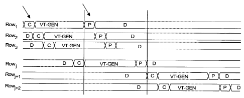
[0039] Figure 2 illustrates an example of the segmented timing schedule for
stable
operation of a light emitting display, in accordance with an embodiment of the
present
invention. In Figure 2, "Rowk" (k=l, 2, 3, ..., j, j+1, j+2) represents a kth
row of a
display array, an arrow shows an execution direction.
[0040] For each row, the timing schedule of Figure 2 includes a compensation
voltage
generation cycle "C", a VT-generation cycle "VT-GEN", a current-regulation
cycle "D",
and a driving cycle "P".
[0041 ] The timing schedule of Figure 2 extends the timing budget of the VT-
generation
cycle "VT-GEN" without affecting the programming time. To achieve this, the
rows of
-6-
CA 02549722 2007-07-25
the display array to which the segmented addressing scheme of Figure 2 is
applied are:
categorized as few segments. Each segment includes rows in which the VT-
generation
cycle is carried out consequently. In Figure 2, Row,, Row2, Row3, ... , and,
Rowj are
in one segment in a plurality of rows of the display array.
[0042] The programming of each segment starts with executing the first and
second
operating cycles "C" and "VT-GEN". After that, the current-calibration cycle
"P" is
preformed for the entire segment. As a result, the timing budget of the VT-
generation
cycle "VT-GEN" is extended to j.iP where j is the number of rows in each
segment, and
Tp is the timing budget of the first operating cycle "C" (or current
regulation cycle).
[0043] Also, the frame time iF is ZxnxiP where n is the number of rows in the
display,
and Z is a function of number of iteration in a segment. For example, in
Figure 2, the
VT generation starts from the first row of the segment and goes to the last
row (the first
iteration) and then the programming starts from the first row and goes to the
last row
(the second iteration). Accordingly, Z is set to 2. If the number of iteration
increases,
the frame time will become ZxnxiP in which Z is the number of iteration and
may be
greater than 2.
[0044] Figure 3 illustrates an example of the parallel timing schedule for
stable
operation of a light emitting light display, in accordance with an embodiment
of the
present invention. In Figure 3, "Rowk" (k=l, 2, 3, ..., j, j+1) represents a
kth row of a
display array.
[0045] Similar to Figure 2, the timing schedule of Figure 3 includes the
compensation
voltage generation cycle "C", the VT-generation cycle "VT-GEN", the
current-regulation cycle "P", and the driving cycle "D", for each row.
[0046] The timing schedule of Figure 3 extends the timing budget of the VT-
generation
cycle "VT-GEN", whereas rP is preserved as iF/n, where ip is the timing budget
of the
first operating cycle "C", TF is a frame time, and n is the number of rows in
the display
array. In Figure 3, Row, to Rowj are in a segment in a plurality of rows of
the display
array.
-7-
CA 02549722 2006-06-08
[0047] According to the above addressing scheme, the current-regulation cycle
"P" of
each segment is preformed in parallel with the first operating cycles "C" of
the next
segment. Thus, the display array is designed to support the parallel
operation, i.e.,
having capability of carrying out different cycles independently without
affecting each
other, e.g., compensation and programming, VT-generation and current
regulation.
[0048] Figure 4 illustrates an example of an example of an AMOLED display
array
structure for the the timing schedules of Figures 2 and 3. In Figure 4, SEL[a]
(a=1, ... ,
m) represents a select signal to select a row, CTRL[b] (b=l, ... , m)
represents a
controlling signal to generate the threshold voltage of the drive TFT at each
pixel in the
row, and VDATA[c] (c=1, ... , n) represents a data signal to provide a
programming
data. The AMOLED display 10 of Figure 4 includes a plurality of pixel circuits
12
which are arranged in row and column, an address driver 14 for controlling
SEL[a] and
CTRL[b], and a data driver 16 for controlling VDATA[c]. The rows of the pixel
circuits 12 (e.g., Row,, ... , Rown,_h and Row,n_h+l, ... , Rown,) are
segmented as
described above. To implement certain cycles in parallel, the AMOLED display
10 is
designed to support the parallel operation.
[0049] Figure 5 illustrates an example of a pixel circuit to the segmented
timing
schedule and parallel timing schedule are applicable. The pixel circuit 50 of
Figure 5
includes an OLED 52, a storage capacitor 54, a drive TFT 56, and switch TFTs
58 and
60. A select line SEL1 is connected to the gate terminal of the switch TFT 58.
A
select line SEL2 is connected to the gate terminal of the switch TFT 60. The
first
terminal of the switch TFT 58 is connected to a data line VDATA, and the
second
terminal of the switch TFT 58 is connected to the gate of the drive TFT 56 at
node Al.
The first terminal of the switch TFT 60 is connected to node A1, and the
second
terminal of the switch TFT 60 is connected to a ground line. The first
terminal of the
drive TFT 56 is connected to a controllable voltage supply VDD, and the second
terminal of the drive TFT 56 is connected to the anode electrode of the OLED
52 at
node B 1. The first terminal of the storage capacitor 54 is connected to node
A1, and the
second terminal of the storage capacitor 54 is connected to node B 1. The
pixel circuit
50 can be used with the segmented timing schedule, the parallel timing
schedule, and a
combination thereof.
-8-
CA 02549722 2006-06-08
[0050] VT-generation occurs through the transistors 56 and 60, while current
regulation
is performed by the transistor 58 through the VDATA line. Thus, this pixel is
capable
of implementing the parallel operation.
[0051] Figure 6 illustrates an example of a timing schedule applied to the
pixel circuit
50. In Figure 7, "Xl l", "X12", "X13", and "X14" represent operating cycles.
Xl l
corresponds to "C" of Figures 2 and 3 , X12 corresponds to "VT-GEN" of Figures
2 and
3, X13 corresponds to "P" of Figures 2 and 3, and Xl4 corresponds to "D" of
Figures
2 and 3.
[0052] Referring to Figures 5 and 6, the storage capacitor 54 is charged to a
negative
voltage (-Vcomp) during the first operating cycle Xl l, while the gate voltage
of the
drive TFT 56 is zero. During the second operating cycle X12, node Bl is
charged up to
-VT where VT is the threshold of the drive TFT 56. This cycle X12 can be done
without
affecting the data line VDATA since it is preformed through the switch
transistor 60,
not the switch transistor 58, so that the other operating cycle can be
executed for the
other rows. During the third operating cycle X13, node A1 is charged to a
programming
voltage Vp, resulting in VGS =VP +VT where VGS represents a gate-source
voltage of the
drive TFT 56.
[0053] Figure 7 illustrates another example of a pixel circuit to the
segmented timing
schedule and the parallel timing schedules are applicable. The pixel circuit
70 of Figure
7 includes an OLED 72, storage capacitors 74 and 76, a drive TFT 78, and
switch TFTs
80, 82 and 84. A first select line SELl is connected to the gate terminal of
the switch
TFTs 80 and 82. A second select line SEL2 is connected to the gate terminal of
the
switch TFT 84. The first terminal of the switch TFT 80 is connected to the
cathode of
the OLED 72, and the second terminal of the switch TFT 80 is connected to the
gate
terminal of the drive TFT 78 at node A2. The first terminal of the switch TFT
82 is
connected to node B2, and the second terminal of the switch TFT 82 is
connected to a
ground line. The first terminal of the switch TFT 84 is connected to a data
line VDATA,
and the second terminal of the switch TFT 84 is connected to node B2. The
first
terminal of the storage capacitor 74 is connected to node A2, and the second
terminal
of the storage capacitor 74 is connected to node B2. The first terminal of the
storage
capacitor 76 is connected to node B2, and the second terminal of the storage
capacitor
-9-
CA 02549722 2006-06-08
76 is connected to a ground line. The first terminal of the drive TFT 78 is
connected to
the cathode electrode of the OLED 72, and the second terminal of the drive TFT
78 is
coupled to a ground line. The anode electrode of the OLED 72 is coupled to a
controllable voltage supply VDD. The pixel circuit 70 has the capability of
adopting
the segmented timing schedule, the parallel timing schedule, and a combination
thereof.
[0054] VT-generation occurs through the transistors 78, 80 and 82, while
current
regulation is performed by the transistor 84 through the VDATA line. Thus,
this pixel
is capable of implementing the parallel operation.
[0055] Figure 8 illustrates an example of a timing schedule applied to the
pixel circuit
70. In Figure 8, "X21", "X22", "X23", and "X24" represent operating cycles.
X21 corresponds to "C" of Figures 2 and 3, X22 corresponds to "VT-GEN" of
Figures
2 and 3, X23 corresponds to "P" of Figures 2 and 3, and X24 corresponds to "D"
of
Figures 2 and 3.
[0056] Referring to Figures 7 and 8, the pixel circuit 70 employs
bootstrapping effect to
add a programming voltage to the stored VT where VT is the threshold voltage
of the
drive TFT 78. During the first operating cycle x21, node A2 is charged to a
compensating voltage, VDD-VOLED where VOLED is a voltage of the OLED 72, and
node
B2 is discharged to ground. During the second operating cycle X22, voltage at
node A2
is changed to the VT of the drive TFT 78. The current regulation occurs in the
third
operating cycle X23 during which node B2 is charged to a programming voltage
Vp so
that node A2 changes to VP+VT.
[0057] The segmented timing schedule and the parallel timing schedule
described
above provide enough time for the pixel circuit to generate an accurate
threshold
voltage of the drive TFT. As a result, it generates a stable current despite
the pixel
aging, process variation, or a combination thereof. The operating cycles are
shared in
a segment such that the programming cycle of a row in the segment is
overlapped with
the programming cycle of another row in the segment. Thus, they can maintain
high
display speed, regardless of the size of the display.
[0058] A shared signaling addressing scheme is described in detail. According
to the
shared signaling addressing scheme, the rows in the display array are divided
into few
-10-
CA 02549722 2006-06-08
segments. The aging factor (e.g., threshold voltage of the drive TFT, OLED
voltage) of
the pixel circuit is stored in the pixel. The stored aging factor is used for
a plurality of
frames. One or more signals required to generate the aging factor are shared
in the
segment.
[0059] For example, the threshold voltage VT of the drive TFT is generated for
each
segment at the same time. After that, the segment is put on the normal
operation. All
extra signals besides the data line and select line required to generate the
threshold
voltage (e.g., VSS of Figure 10) are shared between the rows in each segment.
Considering that the leakage current of the TFT is small, using a reasonable
storage
capacitor to store the VT results in less frequent compensation cycle. As a
result, the
power consumption reduces dramatically.
[0060] Since the VT-generation cycle is carried out for each segment, the time
assigned
to the VT-generation cycle is extended by the number of rows in a segment
leading to
more precise compensation. Since the leakage current of a-Si: TFTs is small
(e.g., the
order of 10-14), the generated VT can be stored in a capacitor and be used for
several
other frames. As a result, the operating cycles during the next post-
compensation
frames are reduced to the programming and driving cycles. Consequently, the
power
consumption associated with the external driver and with charging/discharging
the
parasitic capacitances is divided between the same few frames.
[0061 ] Figure 9 illustrates an example of the shared signaling addressing
scheme for a
light emitting light display, in accordance with an embodiment of the present
invention.
The shared signaling addressing scheme reduces the interface and driver
complexity.
[0062] A display array to which the shared signaling addressing scheme is
applied is
divided into few segments, similar to those for Figures 2 and 3. In Figure 9,
"Row [j,
k]" (k=l, 2, 3, ... , h) represents the kth row in the j'h segment,"h" is the
number of row
in each segment, and "L" is the number of fra.mes that use the same generated
VT. In
Figure 9, "Row [j, k]" (k=1, 2, 3, ... , h) is in a segment, and "Row [j-1,
k]" (k=1, 2, 3,
..., h) is in another segment.
[0063] The timing schedule of Figure 9 includes compensation cycles "C & VT-
GEN"
(e.g. 301 of Figure 9), a programming cycle "P", and a driving cycle "D". A
-11-
CA 02549722 2006-06-08
compensation interval 300 includes a generation framp cycle 302 in which the
threshold
voltage of the drive TFT is generated and stored inside the pixel,
compensation cycles
"C & VT-GEN" (e.g. 301 of Figure 9), besides the normal operation of the
display, and
L-1 post compensation frames cycles 304 which are the normal operation frame.
The
generation frame cycle 302 includes one programming cycle "P" and one driving
cycle
"D". The L-1 post compensation frames cycle 304 includes a set of the
programming
cycle "P" and the driving cycle "D", in series.
[0064] As shown in Figure 9, the driving cycle of each row starts with a delay
of iP from
the previous row where iP is the timing budget assigned to the programming
cycle "P".
The timing of the driving cycle "D" at the last frame is reduced for each rows
by i*iP
where "i" is the number of rows before that row in the segment (e.g., (h-1)
for Row
h]).
[0065] Since iP (e.g., the order of 10 s) is much smaller than the frame time
(e.g., the
order of 16 ms), the latency effect is negligible. However, to minimize this
effect, the
programming direction may be changed each time, so that the average brightness
lost
due to latency becomes equal for all the rows or takes into consideration this
effect in
the programming voltage of the frames before and after the compensation
cycles. For
example, the sequence of programming the row may be changed after each
VT-generation cycle (i.e., programming top-to-bottom and bottom-to-top
iteratively),
[0066] Figure 10 illustrates an example of a pixel circuit to which the shared
signaling
addressing scheme is applicable. The pixel circuit 90 of Figure 10 includes an
OLED
92, storage capacitors 94 and 96, a drive TFT 98, and switch TFTs 100, 102 and
104.
The pixel circuit 90 is similar to the pixel circuit 70 of Figure 7. The drive
TFT 98, the
switch TFT 100, and the first storage capacitor 94 are connected at node A3.
The
switch TFTs 102 and 104, and the first and second storage capacitors 94 and 96
are
connected at node B3. The OLED 92, the drive TFT 98 and the switch TFT 100 are
connected at node C3. The switch TFT 102, the second storage capacitor 96, and
the
drive TFT 98 are connected to a controllable voltage supply VSS.
[0067] Figure 11 illustrates an example of a timing schedule applied to the
pixel circuit
90. In Figure 11, "X31", "X32", "X33", "X34", and "X35" represent operating
cycles.
-12-
CA 02549722 2006-06-08
X31, X32 and X33 correspond to the compensation cycles (e.g. 301 of Figure 9),
X34
corresponds to "P" of Figure 9, and X35 correspond to "D" of Figure 9.
[0068] Referri.ng to Figures 10 and 11, the pixel circuit 90 employs a
bootstrapping
effect to add the programming voltage to the generated VT where VT is the
threshold
voltage of the drive TFT 98. The compensation cycles (e.g. 301 of Figure 9)
include the
first three cycles X3 1, X32, and X33. During the first operating cycle X3 1,
node A3 is
charged to a compensation voltage, VDD-VOLED. The timing of the first
operating cycle
X31 is small to control the effect of unwanted emission. During the second
operating
cycle X32, VSS goes to a high positive voltage V 1(for example, V 1= 20 V),
and thus
node A3 is bootstrapped to a high voltage, and also node C3 goes to V1,
resulting in
turning off the OLED 92. During the third operating cycle X33, the voltage at
node A3
is discharged through the switch TFT 100 and the drive TFT 98 and settles to
V2+VT
where VT is the threshold voltage of the drive TFT 98, and V2 is, for example,
16 V.
VSS goes to zero before the current-regulation cycle, and node A3 goes to VT.
A
programming voltage VPG is added to the generated VT by bootstrapping during
the
fourth operating cycle X34. The current regulation occurs in the fourth
operating cycle
X34 during which node B3 is charged to the programming voltage VPG (for
example,
VPG =6V). Thus the voltage at node A3 changes to VPG+VT resulting in an
overdrive
voltage independent of VT. The current of the pixel circuit during the fifth
cycle X35
(driving cycle) becomes independent of VT shift. Here, the first storage
capacitor 94 is
used to store the VT during the VT-generation interval.
[0069] Figure 12 illustrates the pixel current stability of the pixel circuit
90 of Figure
10. In Figure 12, "AVT" represents the shift in the threshold voltage of the
drive TFT
(e.g., 98 of Figure 10), and "Error in lpixel (%)" represents the change in
the pixel
current causing by AVT As shown in Figure 12, the pixel circuit 90 of Figure
10
provides a highly stable current even after a 2-V shift in the VT of the drive
TFT.
[0070] Figure 13 illustrates another example of a pixel circuit to which the
shared
signaling addressing scheme is applicable. The pixel circuit 110 of Figure 13
is similar
to the pixel circuit 90 of Figure 10, and, however, includes two switch TFTs.
The pixel
circuit 110 includes an OLED 112, storage capacitors 114 and 116, a drive TFT
118,
and switch TFTs 120 and 122. The drive TFT 118, the switch TFT 120, and the
first
-13-
CA 02549722 2006-06-08
storage capacitor 114 are connected at node A4. The switch TFTs 122 and the
first and
second storage capacitors 114 and 116 are connected at node B4. The cathode of
the
OLED 112, the drive TFT 118 and the switch TFT 120 are connected to node C4.
The
second storage capacitor 116 and the drive TFT 118 are connected to a
controllable
voltage supply VSS.
[0071 ] Figure 14 illustrates an example of a timing schedule applied to the
pixel circuit
110. In Figure 15, "X41", "X42", "X43", "X44", and "X44" represent operating
cycles.
X41, X42, and X43 correspond to compensation cycles (e.g. 301 of Figure 9),
X44
correspond to "P" of Figure 9, and X45 correspond to "D" of Figure 9.
[0072] Referring to Figures 13 and 14, the pixel circuit 110 employs a
bootstrapping
effect to add the programming voltage to the generated VT. The compensation
cycles
(e.g. 301 of Figure 9) include the first three cycles X41, X42, and X43.
During the first
operating cycle X41, node A4 is charged to a compensation voltage, VDD-VOLED.
The
timing of the first operating cycle X41 is small to control the effect of
unwanted
emission. During the second operating cycle X42, VSS goes to a high positive
voltage
V l(for example, V 1= 20 V), and so node A4 is bootstrapped to a high voltage,
and also
node C4 goes to V 1, resulting in turning off the OLED 112. During the third
operating
cycle X43, the voltage at node A4 is discharged through the switch TFT 120 and
the
drive TFT 118 and settles to V2+ VT where VT is the threshold voltage of the
drive TFT
118 and V2 is, for example, 16 V. VSS goes to zero before the current-
regulation cycle,
and thus node A4 goes to VT. A programming voltage VPG is added to the
generated
VT by bootstrapping during the fourth operating cycle X44. The current
regulation
occurs in the fourth operating cycle X44 during which node B4 is charged to
the
programming voltage VPG (for example, VPG = 6 V). Thus the voltage at node A4
changes to VPG+VT resulting in an overdrive voltage independent of VT. The
current
of the pixel circuit during the fifth cycle X45 (driving cycle) becomes
independent of
VT shift. Here, the first storage capacitor 114 is used to store the VT during
the
VT-generation interval.
[0073] Figure 15 illustrates an example of an AMOLED display structure for the
pixel
circuit of Figure 10. In Figure 15, GSEL[a] (a=l, ... , k) corresponds to SEL2
of Figure
10, SEL1 [b] (b=l, ... , m) corresponds to SEL1 of Figure 10, GVSS[c] (c=1,
... , k)
-14-
CA 02549722 2006-06-08
corresponds to VSS of Figure 10, VDATA[d] (d=1, ..,. , n) corresponds to VDATA
of
Figure 10. The AMOLED display 200 of Figure 15 includes a plurality of pixel
circuits
90 which are arranged in row and column, an address driver 204 for controlling
GSEL[a], SEL1 [b] and GVSS[c], and a data driver 206 for controlling VDATA[s].
The
rows of the pixel circuits 90 are segmented as described above. In Figure 15,
segment
[ 1] and segment [k] are shown as examples.
[0074] Referring to Figures 10 and 15, SEL2 and VSS signals of the rows in one
segment are connected together and form GSEL and GVSS signals.
[0075] Figure 16 illustrates an example of an AMOLED display structure for the
pixel
circuit of Figure 14. In Figure 17, GSEL[a] (a=1, ... , k) corresponds to SEL2
of Figure
14, SELI [b] (b=1, ... , m) corresponds to SEL1 of Figure 14, GVSS[c] (c=1,
... , k)
corresponds to VS S of Figure 14, VDATA[d] (d= 1, ... , n) corresponds to
VDATA of
Figure 14. The AMOLED display 210 of Figure 16 includes a plurality of pixel
circuits
110 which are arranged in row and column, an address driver 214 for
controlling
GSEL[a], SEL1 [b] and GVSS[c], and a data driver 216 for controlling VDATA[s].
The
rows of the pixel circuits 110 are segmented as described above. In Figure 15,
segment
[1] and segment [k] are shown as examples.
[0076] Referring to Figures 14 and 16, SEL2 and VSS signals of the rows in one
segment are connected together and form GSEL and GVSS signals.
[0077] Referring to Figures 15 and 16, the display arrays can diminish its
area by
sharing VSS and GSEL signals between physically adjacent rows. Moreover, GVSS
and GSEL in the same segment are merged together and form the segment GVSS and
GSEL lines. Thus, the controlling signals are reduced. Further, the number of
blocks
driving the signals is also reduced resulting in lower power consumption and
lower
implementation cost.
[0078] Figure 17 illustrates a further example of a pixel circuit to which the
shared
signaling addressing scheme is applicable. The pixel circuit of Figure 17
includes an
OLED 132, storage capacitors 134 and 136, a drive TFT 138, and switch TFTs
140, 142
and 144. A first select line SEL is connected to the gate terminal of the
switch TFT 142.
A second select line GSEL is connected to the gate terminal of the switch TFT
144. A
-15-
CA 02549722 2006-06-08
GCOMP signal line is connected to the gate terminal of the switch TFT 140. The
first
terminal of the switch TFT 140 is connected to node A5, and the second
terminal of the
switch TFT 140 is connected to node C5. The first terminal of the drive TFT
138 is
connected to node C5 and the second terminal of the drive TFT 138 is connected
to the
anode of the OLED 132. The first terminal of the switch TFT 142 is connected
to a data
line VDATA, and the second terminal of the switch TFT 142 is connected to node
B5.
The first terminal of the switch TFT 144 is connected to a voltage supply VDD,
and the
second terminal of the switch TFT 144 is connected to node C5. The first
terminal of
the first storage capacitor 134 is connected to node A5, and the second
terminal of the
first storage capacitor 134 is connected to node B5. The first terminal of the
second
storage capacitor 136 is connected to node B5, and the second terminal of the
second
storage capacitor 136 is connected to VDD.
[0079] Figure 18 illustrates an example of a timing schedule applied to the
pixel circuit
130. In Figure 18, operating cycles X51, X52, X53, and X54 form a generating
frame
cycle (e.g., 302 of Figure 9), the second operating cycles X53 and X54 form a
post-compensation frame cycle (e.g., 304 of Figure 9). X53 and X54 are the
normal
operation cycles whereas the rest are the compensation cycles.
[0080] Referring to Figures 17 and 18, the pixel circuit 130 employs
bootstrapping
effect to add a programming voltage to the generated VT where VT is the
threshold
voltage of the drive TFT 138. The compensation cycles (e.g. 301 of Figure 9)
include
the first two cycles X51 and X52. During the first operating cycle X51, node
A5 is
charged to a compensation voltage, and node B5 is charged to VREF through the
switch
TFT 142 and VDATA. The timing of the first operating cycle X51 is small to
control
the effect of unwanted emission. During the second operating cycle X52, GSEL
goes to
zero and thus it turns off the switch TFT 144. The voltage at node A5 is
discharged
through the switch TFT 140 and the drive TFT 138 and settles to VOLED+VT where
VOLED is the voltage of the OLED 132, and VT is the threshold voltage of the
drive TFT
138. During the programming cycle, i.e., the third operating cycle X53, node
B5 is
charged to VP +VREF where VP is a programming voltage. Thus the gate voltage
of the
drive TFT 138 becomes VOLED+VT+VP. Here, the first storage capacitor 134 is
used to
store the VT+VOLED during the compensation interval.
-16-
CA 02549722 2006-06-08
[0081] Figure 19 illustrates an example of an AMOLED display array structure
for the
pixel circuit 130 of Figure 17. In Figure 19, GSEL[a] (a=1, ..., k)
corresponds to GSEL
of Figure 17, SEL[b] (b=1, ..., m) corresponds to SELl of Figure 17, GCMP[c]
(c=1, ...,
k) corresponds to GCOMP of Figure 17, VDATA[d] (d=1, .., n) corresponds to
VDATA of Figure 17. The AMOLED display 220 of Figure 19 includes a plurality
of
pixel circuits 130 which are arranged in row and column, an address driver 224
for
controlling SEL[a], GSEL[b], and GCOMP[c], and a data driver 226 for
controlling
VDATA[c]. The rows of the pixel circuits 130 are segmented (e.g., segment [1]
and
segment [k]) as described above.
[0082] As shown in Figures 17 and 19, GSEL and GCOMP signals of the rows in
one
segment are connected together and form GSEL and GCOMP lines. GSEL and
GCOMP signals are shared in the segment. Moreover, GVSS and GSEL in the same
segment are merged together and form the segment GVSS and GSEL lines. Thus,
the
controlling signals are reduced. Further, the number of blocks driving the
signals is also
reduced resulting in lower power consumption and lower implementation cost.
[0083] Figure 20 illustrates a further example of a pixel circuit to which the
shared
addressing scheme is applicable. The pixel circuit 150 of Figure 20 is similar
to the
pixel circuit 130 of Figure 17. The pixel circuit 150 includes an OLED 152,
storage
capacitors 154 and 156, a drive TFT 158, and switch TFTs 160, 162, and 164.
The gate
terminal of the switch TFT 164 is connected to a controllable voltage supply
VDD,
rather than GSEL. The drive TFT 158, the switch TFT 162 and the first storage
capacitor 154 are connected at node A6. The switch TFT 162 and the first and
second
storage capacitors 154 and 156 are connected at node B6. The drive TFT 158 and
the
switch TFTs 160 and 164 are connected to node C6.
[0084] Figure 21 illustrates an example of a timing schedule applied to the
pixel circuit
150. In Figure 21, operating cycles X61, X62, X63, and X64 form a generating
frame
cycle (e.g., 302 of Figure 9), the second operating cycles X63 and X64 form a
post-compensation frame cycle (e.g., 304 of Figure 9).
[0085] Referring to Figures 20 and 21, the pixel circuit 150 employs
bootstrapping
effect to add a programming voltage to the generated VT where VT is the
threshold
-17-
CA 02549722 2006-06-08
voltage of the drive TFT 158. The compensation cyclos (e.g. 301 of Figure 9)
include
the first two cycles X61 and X62. During the first operating cycle X6 1, node
A6 is
charged to a compensation voltage, and node B6 is charged to VREF through the
switch
TFT 162 and VDATA. The timing of the first operating cycle x61 is small to
control
s the effect of unwanted emission. During the second operating cycle x62, VDD
goes to
zero and thus it turns off the switch TFT 164. The voltage at node A6 is
discharged
through the switch TFT 160 and the drive TFT 158 and settles to VOLED+VT where
VOLED is the voltage of the OLED 152, and VT is the threshold voltage of the
drive TFT
158. During the programming cycle, i.e., the third operating cycle x63, node
B6 is
charged to VP +VREF where Vp is a programming voltage. It has been identified
Thus the
gate voltage of the drive TFT 158 becomes VOLED+VT+VP. Here, the first storage
capacitor 154 is used to store the VT+VOLED during the compensation interval.
[0086] Figure 22 illustrates an example of an AMOLED display array structure
for the
pixel circuit 150 of Figure 20. In Figure 22, SEL[a] (a=1, ..., m)corresponds
to SEL of
Figure 22, GCMP[b] (b=1, ..., K) corresponds to GCOMP of Figure 22, GVDD[c]
(c=1,
..., k) corresponds to VDD of Figure 22, and VDATA[d] (d=1, .., n) corresponds
to
VDATA of Figure 22. The AMOLED display 230 of Figure 22 includes a plurality
of
pixel circuits 150 which are arranged in row and column, an address driver 234
for
controlling SEL[a], GCOMP[b], and GVDD[c], and a data driver 236 for
controlling
VDATA[c]. The rows of the pixel circuits 230 are segmented (e.g., segment [1]
and
segment [k]) as described above.
[0087] Referring to Figures 20 and 22, VDD and GCOMP signals of the rows in
one
segment are connected together and form GVDD and GCOMP lines. GVDD and
GCOMP signals are shared in the segment. Moreover, GVDD and GCOMP in the same
segment are merged together and form the segment GVDD and GCOMP lines. Thus,
the controlling signals are reduced. Further, the number of blocks driving the
signals is
also reduced resulting in lower power consumption and lower implementation
cost.
[0088] According to the embodiments of the present invention, the operating
cycles are
shared in a segment to generate an accurate threshold voltage of the drive
TFT. It
reduces the power consumption and signals, resulting in lower implementation
cost.
The operating cycles of a row in the segment are overlapped with the operating
cycles
-18-
CA 02549722 2006-06-08
of another row in the segment. Thus, they can maintain high display speed,
regardless
of the size of the display.
[0089] The accuracy of the generated VT depends on the time allocated to the
VT-generation cycle. The generated VT is a function of the storage capacitance
and
drive TFT parameters, as a result, the special mismatch affects the generated
VT
associated within the mismatch in the storage capacitor for a given threshold
voltage of
the drive transistor. Increasing the time of the VT-generation cycle reduces
the effect of
special mismatch on the generated VT. According to the embodiments of the
present
invention, the timing assigned to VT is extendable without either affecting
the frame
rate or reducing the number of rows, thus, it is capable of reducing the
imperfect
compensation and spatial mismatch effect, regardless of the size of the panel.
[0090] The VT-generation time is increased to enable high-precision recovery
of the
threshold voltage VT of the drive TFT across its gate-source terminals. As a
result, the
uniformity over the panel is improved. In addition, the pixel circuits for the
addressing
schemes have the capability of providing a predictably higher current as the
pixel ages
and so as to compensate for the OLED luminance degradation.
[0091 ] According to the embodiments of the present invention, the addressing
schemes
improve the backplane stability, and also compensate for the OLED luminance
degradation. The overhead in power consumption and implementation cost is
reduced
by over 90% compared to the existing compensation driving schemes.
[0092] Since the shared addressing scheme ensures the low power consumption,
it is
suitable for low power applications, such as mobile applications. The mobile
applications may be, but not limited to, Personal Digital Assistants (PDAs),
cell phones,
etc.
[0093] All citations are hereby incorporated by reference.
[0094] The present invention has been described with regard to one or more
embodiments. However, it will be apparent to persons skilled in the art that a
number
of variations and modifications can be made without departing from the scope
of the
invention as defmed in the claims.
-19-