Note: Descriptions are shown in the official language in which they were submitted.
CA 02549808 2006-06-08
- 1 - 2005P07776 US-rai
Circuit arrangement and method for detecting a crest factor of
a lamp current or a lamp operating voltage of an electric lamp
Field of the invention
The invention relates to a circuit arrangement for detecting a
crest factor of a lamp current or a lamp operating voltage of
an electric lamp. Furthermore, the invention relates to a
method for detecting such a crest factor. In addition, the
invention also relates to an electronic ballast having a
circuit arrangement for detecting an abovementioned crest
factor and a method for operating an electric lamp using an
electronic ballast, in which a crest factor is detected in
accordance with the abovementioned method.
Background of the invention
When dimming electric lamps, in particular fluorescent lamps
having electronic ballasts, an oscillation can typically be
formed in the lower region of the dimming range, in particular
in the lower third of the dimming range, and this oscillation
results owing to the interaction of the lamp characteristic,
the resonant circuit and the regulation. This range, which is
also referred to as the "frequency reversal" range, occurs to a
particularly severe extent during a runup phase of amalgam
lamps. At extreme ambient temperatures, such a "frequency
reversal" range is also observed in the case of mercury lamps.
This oscillation brings about severe modulation of the lamp
current at frequencies of from 30 Hz to 10 kHz and cannot
usually be recognized as optical instability. The high crest
factor of the lamp current which is caused thereby can,
however, result in severe damage to the electric lamp and have
a life-shortening effect.
In order to avoid operation with a high lamp current crest
factor, attempts are made to keep the range of "frequency
reversal" small by means of suitably selecting the resonant
CA 02549808 2006-06-08
2005P07776 US - 2 -
circuit and the regulation and to reduce the damaging effect of
the high crest factor by means of increased lamp filament
heating. Furthermore, either the range for the permissible
ambient temperature for the dimming operation is restricted or
the permissible dimming range at extreme ambient temperatures
is reduced. In addition, it is also known in the case of some
operating devices, in particular electronic ballasts, for
amalgam lamps for the full dimming function to be released only
after a predetermined period of time after they have been
switched on, in order, as a result, to bridge the runup phase.
Summary of the Invention
The present invention is therefore based on the object of
providing a circuit arrangement for detecting a crest factor of
a lamp current or a lamp operating voltage of an electric lamp
and a method for detecting such a crest factor, by means of
which circuit arrangement and method it is possible to prevent
an electric lamp from being operated at a high crest f actor.
Furthermore, one object of the invention is to provide an
electronic ballast which has a circuit arrangement for
detecting a crest factor of an electric lamp, and a method for
operating an electric lamp using an electronic ballast, with
which the damaging effect of an excessively high crest f actor
on an electric lamp can be prevented and reliable and safe
operation of the electric lamp can be made possible.
A circuit arrangement according to the invention for detecting
a crest factor of an electric lamp is designed both to detect a
lamp current crest factor and a lamp operating voltage crest
factor. The circuit arrangement has a first subcircuit, this
first subcircuit being designed to determine an averaged value
from an input signal applied to the circuit arrangement.
Furthermore, the circuit arrangement comprises a second
subcircuit, which is designed to determine a maximum value from
the input signal applied to the circuit arrangement. As a
CA 02549808 2006-06-08
2005P07776 US - 3 -
further essential feature, the circuit arrangement has a
comparator circuit, the comparator circuit being designed to
produce an output signal in the form of a comparison signal.
The comparison signal which can be produced by the comparator
circuit can in this case be produced from the output signal of
the first subcircuit characterizing the averaged value and from
an output signal of the second subcircuit characterizing the
maximum permissible crest factor. The output signal of the
second subcircuit can be produced whilst taking into account
the signal characterizing the maximum value for the input
signal. The circuit arrangement according to the invention is
thus designed such that operation of an electric lamp with a
high crest factor, in particular a high lamp current crest
factor or a high lamp operating voltage crest factor, can be
prevented. As a result, it is also possible to achieve a
situation in which the electric lamp can be prevented from
being impaired in a damaging and life-shortening manner. Owing
to the circuit arrangement in accordance with the invention, it
is possible to avoid the setting and operation of an electric
lamp being influenced in an interfering manner by means of a
"frequency reversal" range.
The first subcircuit is advantageously in the form of a
low-pass filter circuit. In one preferred embodiment, the
low-pass filter circuit in this case comprises a resistor and a
capacitor, which are electrically connected to a first circuit
node of the first subcircuit. Furthermore, in one preferred
embodiment, the capacitor can be connected at a second
electrical connection to ground potential.
An output of the first subcircuit is preferably elect rically
connected to a first input of the comparator circuit and an
output of the second subcircuit is electrically connected to a
second input of the comparator circuit. The output signals of
the first and the second subcircuits are thus applied to
different inputs of the comparator circuit, which is
advantageously in the form of a comparator.
CA 02549808 2006-06-08
2005P07776 US - 4 -
The second subcircuit is advantageously electrically connected
to a first input connection of the circuit arrangement and, in
a preferred embodiment, comprises a diode and a capacitor,
which are electrically connected to a first circuit node of the
second subcircuit.
The second subcircuit is preferably designed to scale the
signal which characterizes the maximum permissible crest factor
and to input a time constant for this signal which
characterizes this maximum permissible crest factor. For this
purpose, provision may advantageously be made for the second
subcircuit to have two resistors. This may make it possible for
the signal characterizing the peak value of the crest factor or
the maximum permissible crest factor to be produced by means of
the adjustment of the time constant in a variable and flexible
manner, even for a relatively long period of time, and in
particular for this signal to be provided at the second input
of the comparator circuit for a relatively long period of time.
A third subcircuit may preferably be provided, this third
subcircuit being designed to condition and rectify the input
signal which is applied to the circuit arrangement. By means of
such signal conditioning and rectification, it is possible for
the detection of the crest factor to be carried out in a
substantially improved and more precise manner.
The third subcircuit has an output which is advantageously
electrically connected to an input of the first subcircuit. The
third subcircuit preferably comprises at least two diodes and a
resistor. As a result, the third subcircuit can be implemented
in a relatively simple and low-complexity manner and an input
signal can be provided which has been conditioned very well for
further processing purposes and rectified. The crest factor of
the lamp current or the lamp operating voltage of the electric
lamp can preferably be detected at least partially digitally.
In one advantageous embodiment, a microprocessor is provided,
CA 02549808 2006-06-08
2005P07776 US - 5 -
in which at least one of the operations which can be carried
out in the subcircuits and/or the comparator circuit can be
carried out digitally.
The comparison signal of the comparator circuit can preferably
be provided for the purpose of setting the crest factor. The
circuit arrangement is thus designed such that the comparison
signal produced by the comparator circuit can be transmitted,
as the output signal of the circuit arrangement, to further
units which are provided for operating and for setting an
electric lamp, and it is thus possible for the crest factor of
a lamp current or a lamp operating voltage to be set in a
precise and safe manner. Safe operation of the electric lamp
can therefore be carried out with little complexity.
One further aspect of the invention relates to an electronic
ballast for an electric lamp which has a circuit arrangement
according to the invention or an advantageous embodiment of the
circuit arrangement according to the invention. This makes it
possible to achieve a situation in which electric lamps in the
form of fluorescent lamps, which are electrically connected to
electronic ballasts, can be operated and set in a reliable
manner. In particular when dimming these fluorescent lamps, it
is thus possible for a damaging or life-shortening effect owing
to a "frequency reversal" range to be prevented, since the
occurrence of high crest factors of the lamp current or the
lamp operating voltage can be avoided.
The circuit arrangement arranged in the electronic ballast is
preferably electrically connected at a first connection to a
first lamp filament. Furthermore, the circuit arrangement is
also electrically connected at this input to a half-bridge
inverter. The electrical wiring of the circuit arrangement in
the electronic ballast is in this case such that a crest factor
can be detected precisely in a simple and reliable manner.
CA 02549808 2006-06-08
2005P07776 US - 6 -
The circuit arrangement in the electronic ballast preferably
has an output, which is electrically connected to a regulating
unit of the electronic ballast. The comparison signal which is
provided as the output signal by the circuit arrangement can
thus be transmitted directly to this regulating unit for
further processing and evaluation purposes and can be provided
for the purpose of setting the lamp parameters and thus also
the crest factor of the electric lamp.
Provision may be made for the electronic ballast to be
electrically connected to a fluorescent lamp, in particular an
amalgam lamp or a mercury lamp, for setting and operation
purposes. Precisely in the case of these lamps, it is thus
possible for safe operation to be carried out without an
excessively high crest factor of the lamp current or the lamp
operating voltage.
In a method according to the invention for detecting a crest
factor of a lamp operating voltage or a lamp current of an
electric lamp by means of a circuit arrangement, an averaged
value is determined from an input signal applied to the circuit
arrangement in a first method step by means of a first
subcircuit. Furthermore, a maximum value is determined from
this input signal applied to the circuit arrangement by means
of a second subcircuit. An output signal characterizing the
maximum permissible crest factor is determined or produced from
the signal characterizing the maximum value by means of the
second subcircuit. From the output signal of the first
subcircuit which characterizes the averaged value and an output
signal of the second subcircuit which characterizes the maximum
permissible crest factor, in a further method step a comparison
of these two signals is carried out. The comparison signal
produced by the comparison is provided as the output signal of
the circuit arrangement. Owing to the method according to the
invention, a crest factor of the lamp current or the lamp
operating voltage can be detected in a simple and precise
manner with little complexity. The comparison signal produced
CA 02549808 2006-06-08
2005P07776 US - 7 -
in the method according to the invention can then be used as
the information signal for further setting and regulation of
lamp parameters, such that the operation of an electric lamp
with an excessively high crest factor of the lamp current or
the lamp operating voltage can be prevented.
The input signal is advantageously conditioned and rectified
prior to the determination of the averaged value.
One further aspect of the invention relates to a method for
operating an electric lamp which is electrically connected to
an electronic ballast, in this method according to the
invention for operating the electric lamp, a crest factor of a
lamp operating voltage or a lamp current being detected in
accordance with an above-explained method according to the
invention for detecting such a crest factor. This makes it
possible to achieve a situation in which the electric lamp can
be operated and set in a safe and reliable manner.
Further refinements of the invention are specified in the
dependent claims.
Advantageous refinements of the circuit arrangement according
to the invention and the electronic ballast according to the
invention are, where transferable, also regarded as refinements
according to the invention of the method according to the
invention for detecting a crest factor of a lamp operating
voltage or a lamp current of an electric lamp and the method
according to the invention for operating an electric lamp.
In the invention, a crest factor of the lamp current or the
lamp operating voltage is thus determined using a suitable
circuit arrangement, which is preferably arranged in an
electronic ballast, using a measurement of the lamp current or
the lamp operating voltage. The determined crest factor is
compared with a permissible maximum value, it being possible,
in the event of the maximum value being exceeded by the
CA 02549808 2006-06-08
2005P07776 US - 8 -
determined value of the crest factor, for a power of the
electric lamp to be increased until the determined value falls
below the permissible maximum value again. It is also possible
with the invention to achieve a situation in which, in critical
phases of operation, in particular during the runup phase of
the electric lamp, the dimming range virtually has a lower
limit, but only as far as is required or only to a minimum
extent.
Brief Description of the Drawings
Exemplary embodiments of the invention will be explained in
more detail below with reference to schematic drawings, in
which;
figure 1 shows a first and second exemplary embodiment of an
electronic ballast according to the invention, which
is connected to an electric lamp; and
figure 2 shows an illustration of a circuit arrangement
according to the invention for detecting a crest
factor of a lamp current or a lamp operating voltage.
Detailed description of the Invention
Identical or functionally identical elements are provided with
the same reference symbols in figures 1 and 2.
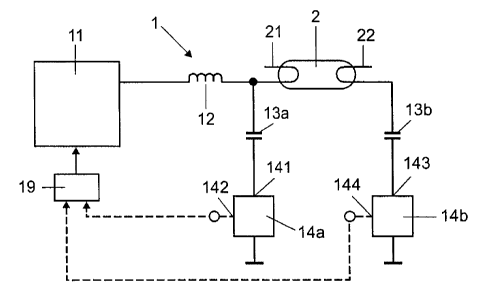
Figure 1 shows a schematic illustration of an electronic
ballast 1. The electronic ballast 1 is electrically connected
to an electric lamp, which, in the exemplary embodiment shown,
is in the form of a fluorescent lamp 2.
The illustration shown in figure 1 shows two different
exemplary embodiments of the invention. First, the
implementation of the first exemplary embodiment will be
explained in more detail below. The electronic ballast 1 has a
CA 02549808 2006-06-08
2005P07776 US - 9 -
half-bridge inverter 11, which is electrically connected at one
output to an inductance 12. The inductance 12 is furthermore
electrically connected to a first lamp filament 21 of the
fluorescent lamp 2. Furthermore, the inductance 12 also has an
electrical connection to a capacitor, which in the exemplary
embodiment is in the form of a starting capacitor 13a. Note
will be made of the fact that the starting capacitor 13a may
also be in the form of an element of a voltage divider circuit
for lamp voltage measurement, which can also be realized in the
form of a resistance divider circuit. Furthermore, the
electronic ballast 1 comprises a circuit arrangement 14a
according to the invention for detecting a crest factor of a
lamp operating voltage which is electrically connected at a
first input 141 to the first lamp filament 21 via the starting
capacitor 13a. In the signal path between the inductance 12 and
the first lamp filament 21 and in the signal path between the
inductance 12 and the circuit arrangement 14a, a signal
characterizing the lamp operating voltage is transmitted.
Furthermore, a further capacitor, which in the exemplary
embodiment is in the form of a half-bridge capacitor 13b, is
connected to a second lamp filament 22. Furthermore, the
half-bridge capacitor 13b in the first exemplary embodiment has
an electrical connection to ground potential. Note will be made
of the fact that, in the first exemplary embodiment, a circuit
arrangement 14b is not provided.
As can also be seen from the illustration in figure 1, the
circuit arrangement 14a has a first output 142, which is
electrically connected to a regulating unit 19. Furthermore,
the circuit arrangement 14a is electrically connected at a
second output to ground potential. The regulating unit 19 is
furthermore electrically connected at one output to an input of
the half-bridge inverter 11. In the first exemplary embodiment
explained above, the circuit arrangement 14a according to the
invention for detecting the crest factor of the lamp operating
voltage is thus formed.
CA 02549808 2006-06-08
2005P07776 US - 10 -
The second exemplary embodiment of the electronic ballast 1
according to the invention, which is likewise illustrated in
figure 1, will be explained in more detail below. Note will be
made of the fact that, in this second exemplary embodiment, the
circuit arrangement 14a is not formed. In this second exemplary
embodiment, the starting capacitor 13a is connected to ground
potential. Instead of the circuit arrangement 14a, in the
second exemplary embodiment the circuit arrangement 14b for
detecting the crest factor of the lamp current is formed. The
circuit arrangement 14b is electrically connected at a first
input 143 to the half-bridge capacitor 13b. In accordance with
the first exemplary embodiment, in the second exemplary
embodiment too, the circuit arrangement 14b has a first output
144, which is electrically connected to the regulating unit 19,
a second output of the circuit arrangement 14b being connected
to ground potential. Mention will be made of the fact that an
electronic ballast 1 according to the invention is realized
either in accordance with the first exemplary embodiment or in
accordance with the second exemplary embodiment. An embodiment
in which both the signal path from the inductance 12 via the
starting capacitor 13a via the circuit arrangement 14a to the
regulating unit 19 and also the signal path from the second
lamp filament 22 via the half-bridge capacitor 13b via the
circuit arrangement 14b to the regulating unit 19 are realized
is not provided.
Figure 2 shows a detailed illustration of a circuit arrangement
14a or 14b according to the invention for detecting a crest
factor of a lamp operating voltage or a lamp current. For a
more detailed explanation, the circuit arrangement 14b for
detecting the crest factor of the lamp current will be
considered in more detail below. As can be seen from figure 2,
the circuit arrangement 14b according to the invention has a
first subcircuit 15, which is designed to determine an averaged
value of the lamp current from an input signal applied to the
circuit arrangement 14b via the input connection 143. The ffirst
subcircuit 15 is, in the exemplary embodiment, in the form of a
CA 02549808 2006-06-08
2005P07776 US - 11 -
low-pass filter circuit and has a resistor 151 and a capacitor
152. The resistor 151 is electrically connected at a ffi rst end
to an input 15b of the first subcircuit 15 and at a second end
to a circuit node of the first subcircuit 15. The capacitor 152
is likewise connected to the circuit node of the first
subcircuit 15 and also has a second electrical connection to
ground potential.
Furthermore, the circuit arrangement 14b comprises a second
subcircuit 16, which, in the exemplary embodiment, is designed
to determine a maximum permissible value of the lamp current
from the input signal applied to the circuit arrangement 14b.
As can be seen, the second subcircuit 16 has an input 16b,
which is electrically connected to the input connection 143 of
the circuit arrangement 14b. In order to produce a maximum
permissible value from the input signal, the second subcircuit
16 has a diode 161 and a capacitor 162. In this case, the diode
161 is connected at its anode to the input 16b of the second
subcircuit 16. With its cathode, the diode 161 is elect rically
connected to a first circuit node of the second subcircuit 16.
The capacitor 162 is also electrically connected to this first
circuit node, this capacitor 162 being electrically connected
at its second end to ground potential. In the exemplary
embodiment shown in figure 2, the second subcircuit 16 also has
two resistors 163, 164, which are designed to scale the signal
and to input a time constant for this signal, which
characterizes the maximum permissible crest factor. As can be
seen from the illustration in figure 2, the resistor 164 is
connected to ground potential and is connected to a second
circuit node of the second subcircuit 16. The first resistor
163 is connected between the two circuit nodes of the second
subcircuit 16. As can be seen from the illustration in figure
2, the first subcircuit 15 is connected at an output 15a to a
first input 17a of a comparator circuit 17. One output 16a of
the second subcircuit 16 is electrically connected to a second
input 17b of this comparator circuit 17. The comparator circuit
CA 02549808 2006-06-08
2005P07776 US - 12 -
17 is, in the exemplary embodiment, in the form of a
comparator.
Furthermore, the circuit arrangement 14b, in the exemplary
embodiment illustrated, comprises a third subcircuit 18, which
is designed to condition and rectify the input signal which is
applied to the input 143. The third subcircuit comp rises a
first diode 181 and a second diode 182. The first diode 181 is
connected at its anode to ground potential, in which case it is
connected at its cathode to a first circuit node of the third
subcircuit. Furthermore, the second diode 182 is connected at
its anode to the first circuit node and at its cathode to a
second circuit node of the third subcircuit 18. Furthermore,
the third subcircuit 18 also comprises a resistor 183, which is
electrically connected to the second circuit node and to ground
potential. As can be seen from the illustration in figure 2, an
output 18a of the third subcircuit 18 is electrically connected
to the input 15b of the first subcircuit 15.
The input signal applied to the input 143 is thus transmitted
to the third subcircuit 18 for conditioning and rectification
purposes. The input signal rectified and conditioned by this
third subcircuit 18 is then transmitted to the first subcircuit
15, in which a signal is generated which characterizes the
averaged value of the lamp current. In a corresponding manner,
the input signal applied to the input 143 is transmitted to the
second subcircuit 16, in which a maximum permissible value is
determined and in which an output signal is produced which
characterizes the maximum permissible crest factor. Then, a
comparison between the output signals of the subcircuits 15 and
16 is carried out in the comparator circuit 17, and the
comparison signal produced by the comparator of the comparator
circuit 17 is provided as the output signal of the circuit
arrangement 14b at the output 144 and is transmitted to the
regulating unit 19. In this regulating unit 19, regulation as
regards a desired value for the crest factor of the lamp
current is then carried out and a corresponding signal is
CA 02549808 2006-06-08
' 2005P07776 US - 13 -
transmitted to the half-bridge inverter 11. By means of the
invention, the fluorescent lamp 2 can be operated without an
excessively high crest factor, in which case it is thus
possible to prevent damaging or life-shortening operation of
the fluorescent lamp 2.
Provision may also be made for at least some of the subcircuits
15, 16 and 18 and/or the comparator circuit 17 to be in the
form of digital circuits and thus for it to be possible for the
respective operations carried out in the subcircuits to be
detected digitally. Provision may be made in a particularly
advantageous manner for the subcircuits 15, 16 and 18 and the
comparator circuit 17 to be realized in a microprocessor and
for the entire detection of the crest factor, as is carried out
in the circuit arrangement 14b, to take place in a digital
manner. This means that the averaging, peak-value detection,
scaling, time response and the threshold value comparison are
carried out on a digital basis.
The circuit arrangement 14a has a similar design to the circuit
arrangement 14b.