Note: Descriptions are shown in the official language in which they were submitted.
CA 02549835 2006-05-25
WO 2005/054838 PCT/US2004/039470
METHOD FOR CONTROLLING ELECTRODEPOSITION OF
AN ENTITY AND DEVICES INCORPORATING
THE IMMOBILIZED ENTITY
Background of the Invention
1. Field of the Invention
The present invention relates to a method and apparatus for controlling
electrodeposition
of an entity, such as a biomolecule, in which the entity is provided in the
vicinity of a. pair of.
electrodes in superposed relationship and a potential is applied across the
electrodes sufficient to
cause migration of the biomolecule component to one of the electrodes and
cause deposition of a
monolayer of the entity on the electrode. The invention further relates to
methods of using the
immobilized entity and to devices incorporating the immobilized entity.
2. Related Art
Conventional methods have been disclosed for immobilizing proteins on a
substrate using
chemical moieties. U.S. Patent No. 6,475,809 describes protein arrays for high
throughpart
screening in which a plurality of different members are immobilized on a
surface of a substrate.
A monolayer is provided on the surface of the substrate. The proteins are
immobilized on the
monolayer. The monolayer is formed of a variety of chemical moieties including
alkysiloxane
monolayers, alklthiol/dialkyldisulfide monolayers and an alkyl monolayer on an
oxide free
silicone substrate.
U.S. Patent No.4,294,677 describes a method for electrodepositing a protein by
electrophoresis onto an ion-exchange-membrane from a liquid in which the
protein is dissolved
or is dispersed in suspension. The ion exchange membrane may comprise
chemically resilient
highly bridged polymeric skeletons on which many anion and canon exchange
groups such as
sulfonate group, carboxylate group, phenol group and ammonium group are
attached as
substituents.
Other conventional methgrls for electrodepositing a protein without using a
chemical
moiety have been described.
U.S. Patent No. 5,166,063 describes a method for immobilizing molecules on a
conductive substrate to produce a biosensor. A biosensor electrode and a
counter electrode are
immersed in a container of a solution of at least one species of biomolecule.
A potential
difference of less than I volt is created between the electrodes. This patent
has the drawback that
CA 02549835 2006-05-25
WO 2005/OSa838 PCT/US2004/039470
because of the relatively large volume used in the system it is difficult to
control the amount of
the biomolecule that is accumulated on the biosensor electrode.
It is desirable to provide a method and system for controlling
electrodeposition of an
entity.
Summary of the Invention
The_ present invention relates to a method and system for controlling
electrodeposition of
a deposition entity in which a solution or suspension of the deposition entity
is provided between
a pair of superposed electrodes at a predetermined concentration. A potential
is applied to the
electrodes sufficient to cause migration of the deposition entity to one of
the electrodes and
deposition of a controll ed thickness of the deposition entity. The distance
between the electrodes
and voltage applied can be controlled to provide migration of the deposition
entity. The method
and system provide controlled immobilization of deposition entities such as
proteins, enzymes,
light harvesting complexes, DNA, RNA, PNA onto a substrate without loss of
function. In one
embodiment, the system can be used on a nanoscale. Additionally, devices can
be formed by the
method of the present invention. The invention will be more fully described by
reference to the
following drawings.
Brief Description of the Drawings
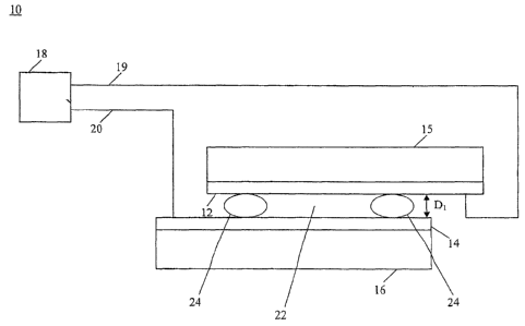
Fig. 1 is a schematic cross sectional view of a system for controlling
electrodeposition of
a deposition entity in accordance with the teachings of the present invention.
Fig. 2 is a top view of a retainer housing of the system shown in Fig. 1 in
combination
with an electrode.
Fig. 3A is a graph of absorption spectra of a deposited film of a deposition
entity
produced by a device according to the present invention.
Fig. 3B is a SEM micrograph of the film shown in Fig. 3A.
Detailed Description
Reference will now be m~.de in greater detail to a preferred embodiment of the
invention,
an example of which is illustrated in the accompanying drawings. Wherever
possible, the same
reference numerals will be used throughout the drawings and the description to
refer to the same
or like parts.
2
CA 02549835 2006-05-25
wo zoosiosasss rcTiuszooaio3ya~o
Fig. 1 is a schematic diagram of a system for controlling electrodeposition of
a deposition
entity l0 in accordance with the teachings of the present invention. System 10
includes
electrode 12 and electrode 14. Electrode 12 and electrode 14 are in a
superposed relation.
Electrodes 12 and 14 can be formed of metals or "metal substitutes." The term
"metal" is
used to embrace both materials composed of an elementally pure metal, such as
Ag or Mg, and
also metal alloys which are materials composed of two or more elementally pure
metals, e.g., Mg
and Ag together, denoted Mg:Ag. The term "metal substitute" refers to a
material that is not a
metal within the normal definition, but which has the metal-like properties
that are desired in
certain appropriate applications. Suitable metal substitutes which can be used
for electrodes 12
and 14 include doped wide bandgap semiconductors, for example, transparent
conducting oxides
such as indium tin oxide (ITO), gallium indium tin oxide (GITO), and zinc
indium tin oxide
(ZITO). Other suitable materials for electrodes 12 and 14 are polymeric metals
such as
poly-ehtylene-dioxythiophene (PEDOT) doped with poly-styrenesulfonate (PSS).
One or more of electrode 12 and electrode 14 can be transparent. As used
herein, a layer .
of material is said to be "transparent" when the layer or layers permit at
least 50% of the ambient
electromagnetic radiation in relevant wavelengths to be transmitted through
the layer or layers.
Similarly, layers which permit some but less than 50% transmission of ambient
electromagnetic
radiation in relevant wavelengths are said to be "semi-transparent". In
particular, ITO is a highly
doped degenerate n~ semiconductor with an optic bandgap of approximately 3.2
eV rendering it
transparent to wavelengths greater than approximately 3900 t~.. Another
suitable metal substitute
material is the transparent conductive polymer polyanaline (PANI) and its
chemical relatives.
Metal substitutes can be further selected from a~wide range of non-metallic
materials,
wherein the term "non-metallic" is meant to embrace a wide range of materials
provided that the
material is free of metal in its chemically uncombined form. When a metal is
present in ifs
chemically uncombined for, either alone or in combination with one or more
other metals as an
alloy, the metal may alternatively,be referred to as being present in its
metallic form or as being a
"free metal". Thus, the metal substitute electrodes of the present invention
may sometimes be
referred to as "metal-free" wherein the term "metal-free" is expressly meant
to embrace a
material free of metal in its chemically uncombined form. Free metals
typically have a form of
metallic bonding that may be thought of as a type of chemical bonding that
results form a sea of
valence electrons which are free to move in an electronic conduction band
throughout the metal
3
CA 02549835 2006-05-25
WO 211U5/U54838 PCT/US2UU4/U3947U
lattice. While metal substitutes may contain metal constituents they are "non-
metallic" on
several bases. The are not pure free-metals nor are they alloys of free-
metals. When metals are
present in their metallic form, the electronic conduction band tends to
provide, among other
metallic properties, a high electrical conductivity as well as a high
reflectivity for optical
radiation.
Electrode IZ can be attached to substrate 15 and electrode 14 can be attached
to
substrate 16. For example, electrode 12 and electrode 14. can be. deposited as
a film on
respective substrate 15 and substrate 16 with known metal and ndn-metal
deposition techniques
such as electron beam evaporation and the like.
Substrates 15 and 16 can be either organic or inorganic, biological or
non.biological, or
any combination of these materials. In one embodiment, the substrate is
transparent or
translucent. Substrates 15 and 16 can be flat, firm or semi-firm. Suitable
materials for
substrates 15 and 16 include silicon, silica, quartz, glass, controlled pore
glass, carbon, alurnina,
titanium dioxide, germanium, silicon nitride, zeolites, and gallium arsenide.
Metals such as gold,
platinum, aluminum copper, titanium, and their alloys are also options for the
substrates. In
addition, many ceramics and polymers can also be used as substrates. Polymers
which can be
used as substrates include, but are not limited to, the following:
polystyrene;
poly(tetra)fluorethylene; (poly)vinylidenedifluoride; polycarbonate;
polymethylmethacrylate;
polyvinlyethylene; polyethyleneimide; poly(etherether) ketone;
polyoxymethylene (POM);
polyvinylphenol; polylactides; polymethacrylimide (PMl); polyalkenesulfone
(PAS);
polyhydroxyethylmethacrylate; polydimethylsiloxane; polyacrylamide; polyimide;
co-block-
polymers; and Eupergit~, Photoresists, polymerized Langmuir~Blodgett films,
and LIGA
structures can also serve as substrates in the present invention. ~ ,
Power supply 18 having positive lead 19 connected to electrode 12 and negative
lead 20
connected to electrode 1~1 is provided to supply substantially constant
current flow between
electrode 12 and electrode 14. .,The direction of current flow can be reversed
if desired by
switching the connections of lead 19 and lead 20 to power supply 18 to make
lead 19 negatively
charged and lead 20 positively charged.
Distance D~ between electrode 12 and electrode 14 can be in the range of about
lOnm to
about S.Omm. In one embodiment, the'distance D, and size of electrode 12 and
electrode 14 are
selected to be useful in nanoscale .devices. Deposition an nanoscale
electrodes can occur
4
CA 02549835 2006-05-25
WO 2005/054838 PCT/US2004/039470
provided the remaining area of the substrate is insulated. A suitable distance
D, is about l.Omm.
The voltage applied to electrode 12 and electrode 14 is_ dependent on the
distance D~. For
example, the voltage applied can be in the range of about 1 V/cm to about
1,000 V/cm. A
suitable voltage range of about 10 V/em to about 200 V/cm can be used with a
distance between
electrode 12 and electrode 14 of about I mm.
A solution or suspension of deposition entity 22 is provided between
electrodes 12
and 14. The voltage is continuously applied far a predetermined time to effect
migration of
deposition entity 22 toward electrode 12 or 14 to provide deposition of a film
of deposition
entity 22 on electrode 12 or electrode 14. For example, voltage can be
continuously applied for
I 0 about 5 minutes to about 48 hours. The .voltages applied are based on the
desired thickness of a
film of deposition entity 22, and on the concentration of the solution from
which deposition
entity 22 is electrodeposited. It has been found desirable to use the smallest
distance between
electrodes 12 and 14 in order to decrease the voltage to provide needed
migration of deposition
entity 22.
The concentration of the deposition entity in solution or suspension of
deposition
entity 22 and the volume of the solution is selected to control the thickness
of a film of
deposition entity 22 that is deposited on electrode 12 or electrode 14 upon
continuous application
of a predetermined voltage. For example, the concentration of the deposition
entity in solution
or suspension of deposition entity 22 can be selected to form a monolayer on
electrode 12 or
electrode 14. In one embodiment of the present invention, 100% of the
deposition entity can be
deposited on electrode 12 or electrode 14 using a concentration of the
deposition entity in the
range of about IOp.g/ml to about 1mg/ml , a volume of about lmm3 to about
lOOmm3 with a
voltage in the iange~of about 10 V/cm to about 200 V/cm resulting in a film of
a monolayer
having a thickness of about Snm to about I Onm. It will be appreciated that
thicker films can be
deposited by varying the concentration of deposition entity 22 in solution or
suspension and the
volume of the solution.
Retainer housing 24 can be used to retain solution or suspension of deposition
entity 22
between electrodes 12 and electrodes 14. Retainer housing 24 is positioned
adjacent
electrode 12 and electrode 14. As shown in Fig. 2, retainer housing 24 can
have open ends, such
as an O-ring. Alternatively, retainer housing 24 can have various shapes.
Retainer housing 24
can have a size selected to provide a predetermined volume of solution or
suspension of '
5
CA 02549835 2006-05-25
WO 2UU5/U5:1838 PCT/US2UU4/03947U
deposition entity 22. For example, retainer housing 24 can have a size to
provide a volume of
about I mm3 to about 1 OOmm3.
In one embodiment, retainer housing 24 can be placed on one electrode fox
example,
electrode 14. Thereafter, a solution or suspension of deposition entity 22 is
received in retainer
housing 24 and contacts electrode 14. The volume of the solution or suspension
of deposition
entity 22 fills retainer housing 24. ~~ The other electrode fox example,
electrode 12 is placed on top
of retainer housing 24 for retaining deposition entity 22 between electrode 12
and electrode 14.
For example, a substrate can be used with retainer housing 24 300mm silicon
wafer on the order
of lOsmm3 to cover the whole substrate with about a lmm thick deposition cell.
Migration of the deposition entity occurs towards the electrode 12 or 14
charged in the
opposite sense to the charge of the deposition entity in solution or
suspension of deposition
entity 22. Upon migration of deposition entity 22 to electrode 12 or electrode
14, deposition
entity 22 can be attached to electrode 12 or 14 largely due to van der Waals
interactions between
the deposition entity and electrode 12 or electrode 14.
. The deposition entity is suitable for deposition on electrodes 12 or 14.
Suitable
deposition entities include but are not limited to the following classes of
naturally occurring or
artificially synthesized molecules or molecular grouping that can exist as
components of
biological systems: proteins including simple proteins and complex proteins
containing other
organic compounds, such as for example apoproteins, glycoproteins, peptides,
oligopeptides,
lipoproteins, ovo-proteins, facto-proteins, serum-proteins, myo-proteins, seed-
proteins,
scleroproteins, chromoproteins, phosphoproteins and nucleo-proteins. Other
suitable deposition
entities include antigens and antibodies thereto, antibody fragments, haptens
and antibodies
thereto, receptors and other membrane proteins, protein analogs in which at
least one non-
peptide linkage replaces a peptide linkage, enzymes and enzyme precursors,
coenzymes, enzyme
inhibitors, amino acids and their derivatives, hormones, lipids,
phospholipids, glycolipids,
liposomes, nucleotides, oligonucleotides, polynucleotides, and their art-
recognized and
biologically functional analogs and derivatives including, for example:
methylated
polynucleotides and nucleotide analogs having phosphorothioate linkages;
plasrnids, cosmids,
artificial chromosomes, other nucleic acid vectors; antisense polynucleotides
including those
substantially complementary to at least one endogenous nucleic acid or those
having sequences
with a sense opposed to at least portions of selected viral or retroviral
genomes, viruses, bacteria
6
CA 02549835 2006-05-25
WO 2005/054838 PCT/US2004/039470
phages, antisense and any other biologically active molecule, synthetic
composite,
macromolecules or synthetic polymers. Suitable deposition entities 22 also
include
deoxyribonucleic acids (DNA), ribonucleic acids (RNA) and peptide nucleic
acids (PNA).
Deposition entity 22 can include a light harvesting complex. The term "Light
Harvesting
Complex" (LHC) as used herein refers to photosynthetic complexes, e.g., PSI
(Photosystem I,
from spinach, for example), PS2 (Photosystem II), LH1 (Light Harvesting
complex 1) andlor
LH2 (Light Harvesting complex 2, from purple bacteria). Fromme, P., et al.,
Biochim. Biophys.
Acta 1365, 175 (1998); Lee, L, et al.,'Phys. Rev. Lett. 79, 3294 (1997);
Schubert, W.D., et al., J.
Mol. Biol. 272, 741-768 (1997). These complexes are available commercially,
for example,
from PROTEIN LABS Inc., 1425 Russ Blvd., Suite T-107C, San Diego, CA 92101.
Any of the
preceding deposition entities having weak or non-existent polarity or
induceable polarity under
the conditions prevailing in system 10 can be covalently linked to an
appropriate charged carrier
to form a charged complex that can be deposited on the electrodes I2 or 14.
Members of the preceding classes of deposition entities and any combination of
specific
members thereof can be placed in solution or in suspension as colloidal
particles in liquid using
art recognized techniques that depend on the composition of the liquid. The
solution or
suspension of deposition entity 22 can be an aqueous solution, such as
physiological saline,
capable of conducting a substantial electrical current. The solution or
suspension can have a
desired pH at a physiological level. The direction, rate of migration, and
rate of deposition of the
deposition entity originally in solution or suspension of deposition entity 22
onto electrodes 12
and 14 can be controlled with great sensitivity by appropriately adjusting the
pH of the solution.
This conttol is based upon use of conventional electrophoretic techniques
applicable to
permanently charged moieties that give the deposition entity a net charge in
the solution
depending on the pH of the solution. The pH at which the deposition entity has
zexo net negative
charge, and thus will not migrate under the influence of an electric field, is
defined as its
isoelectric point. At pH values greater than the isoelectric point; the
molecule has a net negative
charge; conversely at pH values less than the isoelectric point, the molecule
has a net positive
charge. Accordingly, in system 10 shown in Fig. 1, the pH of the solution or
suspension of
deposition entity 22 is adjusted to greater than or less than the isoelectric
point of the deposition
entity to be deposited on electrodes 12 or I4. This adjustment can be
accomplished using known
7
CA 02549835 2006-05-25
WO 2U115/U54838 PCT/US2UU4/U3947U
acids or alkaline agents as desired. Other additives, such as non-ionic
surfactants and anti-
foaming agents or detergents can also be added to the solution as desired.
Immobilized deposition entities produced according to the method and system of
the
invention can be used in a wide variety of molecular detection systems,
including amperometric
S electrochemical biosensors, calorimeMc, acoustic, potentiometric, optical,
and ISFET based
biosensors.
Immobilized entities such as proteins, enzymes, antibodies, or glycoproteins
such as
lectins can be used in biosensors that detect the presence or concentration of
selected
physiological molecules as a result of the interaction of the physiological
ligand with the
immobilized biomolecules.
Immobilized entities can be used in any device in which the immobilized entity
is
essential to operation of the device. Suitable devices include solid state
devices, memory devices
and photo voltaic devices.
Fig. 3A illustrates absorption spectra of a film of LI-I2 deposited onto an
electrode. A
pair of electrodes had about lmm electrode separation. A voltage of about 50
volts was applied
for 24 hours at room temperature. The absorption spectra shows peaks at 800nm
and 850nm are
clearly visible indicating the complexes are intact (the absorption of
unassociated pigment
molecules would be blue shifted).
Fig. 3B is a SEM micrograph of the resulting film. The I Onm - l5nm sized
features are
the complexes of interest.
It is to be understood that the above-described embodiments are illustrative
of only a few
of the many possible specific embodiments which can represent applications of
the principles of
the invention. Numerous and varied other arrangements can be readily devised
in accordance
with these principles by those skilled in the art without departing from the
spirit and scope of the
invention.
8