Note: Descriptions are shown in the official language in which they were submitted.
CA 02549981 2006-06-13
_..____.__.__ -_.__..~_._ ___._ ~_ _.__ _____.~____ _....____-_______._
__.__._.__.___ _ ._... .... _ _._.. ..
Atty. Dkt. No.: 081149-0115
ARTICLE HAVING PATTERNED DECORATIVE COATING
BACKGROUND
[0001] The present invention relates generally to articles having decorative
coatings
or finishes provided thereon and methods of producing such articles. More
specifically, the present invention relates to articles and methods for
producing
articles which have mufti-tone coatings provided thereon.
[0002) Colored coatings have been provided on articles using physical vapor
deposition (PVD) or chemical vapor deposition (CVD) methods. PVD coatings are
at
present available in a range of colors on such commercial products as plumbing
products, home hardware such as doorlmobs and hinges, automotive products,
recreational products, and various other products.
[0003] PVD and CVD decorative coatings in general offer many performance
advantages such as high hardness, abrasion resistance, corrosion resistance,
chemical
resistance, etc. as compared to conventional polymer and electroplated
coatings.
Although PVD and CVD coatings are available in a variety of colors, presently
available PVD and CVD coatings generally have a uniform color over the entire
substrate surface. It may be desirable, however, for certain applications to
use a PVD
or CVD coating having a visibly-patterned, mufti-color appearance (e.g., for
creating
products having, for example,~streaked, speckled, marbled, "antique", "aged",
or
"distressed" finishes, or having decorative or informational digitized images
incorporated into the surface finish).
[0004) Conventional methods for creating patterned decorative finishes on
products
such as those mentioned above generally utilize polymer coatings for either
coloration
or protection. It is known to use paints, lacquers, etc. to create patterned
finishes
directly on a substrate surface. It is also known to thermally, chemically,
and/or
mechanically treat substrate surfaces to produce patterned finishes, but such
treated
-1-
oo~.~nu~s
CA 02549981 2006-06-13
.._.__ __.~_-_-. ... . -_._ _ ____.._.... _ .. _._ . _ _ ...._... _.___-
._______,.. . _. .__.. ___
Atty. Dkt. No.: 081149-0115
surfaces are often not durable and require a polymer topcoat for protection
against
abrasion and corrosion. Polymer coatings may be susceptible to abrasion,
solvents,
and household chemicals, and may develop pinholes through which corrosion of
the
substrate can initiate.
[0005] PVD coatings, in contrast, are generally very hard and resistant to
abrasion
and chemical attack, and are superior to polymer-based coatings for many
applications. While patterned PVD and CVD coatings have been used in the
electronics industry for purposes of fabricating printed and integrated
circuits, such
coatings have not conventionally been used to provide decorative coatings
(e.g.,
visibly patterned, multi-colored decorative coatings). Such patterned PVD and
CVD
coatings are generally made of materials selected for their electronic (as
opposed to
decorative) properties and are used to produce non-decorative patterns that
are too
small to be visible to the human eye without magnification. In addition, such
patterning processes often handle only flat substrates and a single substrate
at a time,
which would be unsuitable for the mass-production of consumer products.
[0006] It would be advantageous to provide a decorative coating or finish for
an
article that is provided using PVD and/or CVD methods that has a patterned
appearance, which will not rub or scrub off in normal use, which is scratch
and
corrosion resistant; can withstand common household chemicals and solvents,
and
does not age or degrade in sunlight or under exposure to outdoor conditions.
It would
also be advantageous to provide articles having decorative coatings which
provide an
aesthetically pleasing appearance that is visible to the unaided human eye and
that are
produced using methods which are suitable for mass-production. It would be
desirable to provide coatings, articles, and methods which exhibit any one or
more of
these or other advantageous features as may be understood by those of ordinary
skill
in the art reviewing this document.
SUMMARY
[0007] An exemplary embodiment relates to an article having a decorative,
visibly
patterned, multi-colored surface appearance that includes a substrate and a
first
-2-
oo~.~n~~
CA 02549981 2006-06-13
c
___ .._ ._._ _. _.... . _.. _.. _ _. ___ _. _ _ ___A~. Dkt. No.: U8 ~ 149-O 11
coating provided by vapor deposition above at least a portion of the
substrate, the
coating comprising a first material having a first color. The coating
comprises a
random arrangement of penetrations through which a portion of an underlying
surface
is visible, the underlying surface comprising a second material having a
second color
that differs from the first color. The penetrations form a decorative pattern
comprising features distinguishable to an unaided human eye.
[0008] Another exemplary embodiment relates to a method for producing an
article
having a decorative coating that includes depositing at least a first coating
layer onto
at least a portion of a surface of a substrate using a physical or chemical
vapor
deposition method in a vacuum chamber at sub-atmospheric pressure, the first
coating
layer comprising a first material having a first color. The method also
includes
patteniing the first coating layer using a non-uniform patterning process to
form a
patterned coating layer having penetrations through which a portion of an
underlying
surface is visible, the underlying surface comprising a second material and
having a
second color that is visually contrasting to the first color. The patterned
first coating
layer comprises a decorative pattern comprising features distinguishable by an
unaided human eye.
[0009] Another exemplary embodiment relates to a method for producing an
article
having a decorative surface that includes depositing a first layer of material
on a
substrate using a vapor deposition method, the first layer of material
comprising a first
material having a first color; depositing a second layer of material on the
first layer of
material using a vapor deposition method, the second layer of material
comprising a
second material having a second color that differs from the first color, and
removing
portions of the second layer of material to foam apertures extending through
the
second layer. The apertures are the apertures arranged in a random
configuration.
Portions of the first layer are visible through the apertures such that a
decorative
pattern is formed on the article.
-3-
oo~.~n44zs
CA 02549981 2006-06-13
_ ._ _. .__. .._ _ _ __ _ A~. Dlct. No.: 081149-0115
BRIEF DESCRIPTION OF THE DRAWINGS
[0010] FIGURE 1 is a photograph of an article having a decorative coating
provided
thereon according to an exemplary embodiment.
[0011] FIGURE 2 is a photograph of an article having a decorative coating
provided
thereon according to an exemplary embodiment.
(0012] FIGURE 3 is a flow diagram illustrating steps in a method of producing
an
article having a decorative coating according to an exemplary embodiment.
[0013] FIGURES 4-9 are schematic cross-sectional views of a portion of an
article
having a decorative coating provided thereon illustrating steps in the
exemplary
method represented by the flow diagram of FIGURE 3.
[0014] FIGURE 10 is a flow diagram illustrating steps in a method of producing
an
article having a decorative coating according to an exemplary embodiment.
[0015] FIGURES 11-15 are schematic cross-sectional views of a portion of an
article having a decorative coating provided thereon illustrating steps in the
exemplary method represented by the flow diagram of FIGURE 10.
[0016] FIGURE 16 is a photograph of an article having a decorative coating
provided thereon according to an exemplary embodiment.
[0017] FIGURE 17 is a photograph of an article having a decorative coating
provided thereon according to an, exemplary embodiment.
[0018] FIGURE 18 is a flow diagram illustrating steps in a method of producing
an
article having a decorative coating according to an exemplary embodiment.
[0019) FIGURES 19-22 are schematic cross-sectional views of a portion of an
article having a decorative coating provided thereon illustrating steps in the
exemplary method represented by the flow diagram of FIGURE 18.
-4-
oo~.~rr~s2s
CA 02549981 2006-06-13
_ .. __ ____ ... __.._ _. .____...______._..._ . ______A~- D>tt. No.: 081149-
0115
DETAILED DESCRIPTION OF EXEMPLARY EMBODII~~iENTS
[0020] According to an exemplary embodiment, an article or product is provided
that includes a decorative .coating with a visibly-patterned, mufti-colored
appearance
provided thereon. Any of a variety of articles or products may be produced
using the
methods described below in the various exemplary embodiments, including, but
not
necessarily limited to, plumbing components (e.g., faucets, handles, nozzles,
sinks,
drain flanges, stop valves, pipes, tub drains, etc:), home hardware (e.g.,
doorknobs,
hinges, drawer/cabinet pulls, etc.), bath hardware (towel bars, safety "grab"
bars,
etc.), windows and doors (e.g., shower doors, etc.), automotive products
(e.g.,
automotive trim parts, emblems, wheel covers, etc.), knives, medical
instruments,
tableware, recreational products, sporting goods (e.g., golf clubs, ice
skates, etc.),
indoor or outdoor lighting products (e.g., lamps; fixtures, etc.) weatherproof
informational signs, and any of a variety of other products or articles. It
should be
noted that the present invention does not pertain to microprocessors or the
fabrication
of electronic chips and the like.
[0021] According to one exemplary embodiment, at least one coating or layer of
material is provided (e.g., deposited using a PVD andlor CVD pmcess) on a
substrate,
after which a masking material is applied on top of the coating. The masking
material
is then patterned by a random or non-uniform modification process, foaming
penetrations (e.g., apertures or holes) which leave a portion of the
underlying coating
exposed. The exposed portion of the coating is subsequently removed by
chemical
etching, leaving randomly or non-uniformly arranged penetrations through which
an
underlying coating layer or substrate surface having a contrasting color is
visible.
[0022] In this manner, an article having a decorative coating with a visibly-
patterned mufti-colored appearance may be provided that includes at least one
coating
material deposited on a substrate by a vacuum deposition process. According to
various exemplary embodiments, the at least one coating may be provided (e.g.,
deposited) by a PVD technique such as cathodic arc evaporation or sputtering,
or by a
CVD method such as hot-filament or ion-beam PECVD.
-5-
001.1774425
CA 02549981 2006-06-13
..__ ._-~._--_ .__...__.._.._._,_____ .._._.....___--.___.___._.-.___.__...-
__._~__-. .._....._.._.._..
Atty. Dkt. No.: 081149-0115
[0023] The coating may be patterned by etching, using the patterned masking
layer
which is resistant to the etching process, to remove the coating in areas
unprotected
by the mask. The masking layer is subsequently removed using a solvent,
uncovering
the un-etched regions of the coating surface. The coating material is selected
to have
a color which is visually contrasting to the underlying surface exposed by the
etching
process. Regions of contrasting color may alternatively be produced by
anodizing or
otherwise chemically or physically modifying the unmasked regions of the
coating in
such a way as to produce regions having a color contrasting from that of the
masked
regions. The underlying surface may be the substrate surface, or may be an
underlying coating layer selected to have a desired decorative appearance
and/or to
provide other desired properties.
[0024) According to other exemplary embodiments, the coating may be patterned
by providing the coating on top of a patterned masking layer having
penetrations
which expose a portion of the substrate surface (or a surface of another
underlying
layer). After providing the coating, the masking layer is dissolved in a
solvent,
thereby loosening and removing the coating material deposited on top of the
masking
material while leaving in place the coating deposited on the portion of the
substrate
surface exposed through the penetrations in the masking layer. This latter
typo of
process may be referred to as a "lift-ofd' process.
[0025] The patterned masking layer that may be used for either an etching or a
lift-
offpmcess may be formed by depositing a layer of a masking material non-
uniformly
on a substrate, as by stenciling, or by depositing the masking material
uniformly over
the substrate surface and subsequently patterning it by a non-uniform removal
process
such as barrel tumbling in finishing media, which removes portions of the
masking
layer, forming penetrations (e.g., apertures or holes) thmugh which portions
of the
underlying surface is exposed. A variety of methods for forming decoratively-
patterned masking layers according to the various exemplary embodiments will
be
described below in more detail.
-6-
oo~.~n4,s~
CA 02549981 2006-06-13
1
__.__.__-_..___.__ . _ ._. ___._.______ __.__.___ ___ _ __-________._...__..__-
_.._____ .__.__
Atty. Dkt. No.: 081149-0115
[0026] As used herein, the term "substrate" refers to all or a portion of an
article
underlying the decorative coating, and may include any surface protection or
preparation layers such as electroplating or polymer basecoats. According to
various
exemplary embodiments, the substrate may include materials such as metals
(e.g.,
brass, zinc, stainless steel, tin, copper, iron-based alloys, etc.), plastics
(e.g., thermoset
or thermoplastic materials such as a polyolefin or a~crylonitrile-butadiene-
styrene
(ABS) material, etc.), ceramics, glasses (e.g., architectural type glass
(e.g.; shower
doors, etc.), and/or composites (e.g., metal matrix materials, polymer
xriatrix
materials, ceramic and glass matrix materials, carbon graphite matrix
materials, fiber
reinforced composites, and the like).
[0027] Substrates may be electroplated with corrosion-resistant and/or surface-
leveling layers comprising, for example, nickel, chromium, copper, cobalt,
zinc,
cadmium, tin, lead, gold, brass, bronze, rhodium, platinum, nickel-tin alloys,
and
other known electroplating materials. Substrates may also include protective
and/or
surface-leveling polymer layers, anodized layers of the substrate material or
of an
applied coating, or any other known surface-preparation material that is
compatible
with vacuum deposition and patterning processes.
[0028] The term "decorative coating" as used herein refers to coatings that
provide a
desired surface appearance to an article (e.g., to coatings that have a
patterned, multi-
colored visual appearance). In some embodiments, in addition to providing a
desired
surface appearance, the decorative coating may also provide various
utilitarian
features such as some degree of abrasion, scratch, tarnish, and/or corrosion
resistance
to an underlying substrate. Such coatings may also be employed for other
functional
purposes, such as to increase the strength of a cutting edge or to improve the
wear
resistance of a surface (e.g., in cases in which the appearance of the coating
contributes to its consumer marketing appeal).
[0029] The terms 'pattern" and "patterned" refer to a coating or mask
comprising a
layer that has penetrations (e.g., apertures or holes) through which an
underlying
coating layer or substrate of a different (e.g., contrasting) color is
visible. The term
oo~.~rr44zs
CA 02549981 2006-06-13
r
__ _._. _.__~ __ _ _ _ __ __ _ . _ __.. _ .. . __. _ -. . _ _ __..__ __
_.__Atty. Dkt. No.: 081149-0115 -_~ .
"visibly-patterned" refers to a patterned coating or layer in which at least
some
features (regions) of the pattern are of sufficient size and/or have suffcient
color
contrast from surrounding features to be readily distinguished by a human eye
without
magnification, for example, but without limitation, features larger than
around 1 mm
extent in least one linear dimension. Such visible features may also be made
up of
smaller dots or shaped pixels which are individually indistinguishable to a
human eye,
but which together form distinguishable features. The term "decorative
pattern"
refers to a pattern selected at least in part ~to have a desired aesthetically
appealing
appearance. The term "informational pattern" refers to a pattern selected to
provide a
visually distinguishable display of text or of a digitized image, which may
also be
decorative.
[0030] The terms "random" and 'ion-uniform" when used herein to refer to the
arrangement of apertures or holes formed in a layer of material is intended to
mean an
arrangement in which the specific locations of apertures or holes is not
predetermined
prior to patterning. Various techniques for obtaining such random or non-
uniform
arrangements are described below in greater detail. Such arrangements are
unlike
those used, for example, in masks used in the manufacture of micropmcessors
and the
like, which have a set or predetermined pattern when provided on a wafer or
the like
(e.g., so that features such as conductive lines, vial, and the like will line
up properly
to provide the desired functionality).
[0031] It should be understood by those reviewing this disclosure that larger
distinguishable patterns (e.g., an image of an animal) may be formed while
using
random patterning techniques. For example, a substrate may be covered with a
mask
having a cutout formed therein. The cutout may have a desired shape (e.g., an
image
of an animal). The portion of the substrate not covered by the mask
(corresponding to
the cutout) may be patterned in a random or non-uniform fashion to have
apertures
extending through the substrate. When the mask is removed, the portion covered
by
the mask will not be patterned (e.g., will not have apertures extending
therethrough)
and the portion of the substrate not covered by the mask will have random or
non-
_g-
oo~.~n4.a~
CA 02549981 2006-06-13
Atty. Dkt. No.: 081149-0115
uniform patterning therein. An observer of the substrate will then see an
image (e.g.,
an animal) defined by the random or non-uniform patterning.
[0032] The term "contrasting color" refers to a second color which is visually
distinguishable from a first color by an unaided human eye under normal
outdoor or
indoor lighting conditions.
[0033] FIGURES 1 and 2 are photographs of articles 10 and 20 produced using a
method 100 for providing decorative coatings or finishes according to an
exemplary
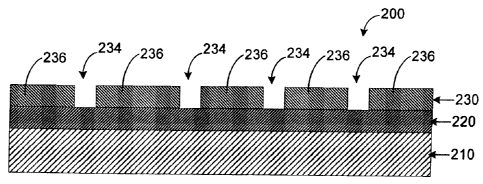
embodiment. FIGURE 3 is a flow diagram illustrating exemplary steps of method
100, and FIGURES 4-9 are schematic cross-sectional views of an article 200
illustrating the steps in method 100.
[0034] In a step' 110 shown in FIGURE 4, a first layer or coating 220
comprising a
material 222 is provided on a substrate 210 comprising a material 212.
According to
an exemplary embodiment, material 222 is a relatively dark-colored material.
For
example, material 222 may be an oxy-carbide or oxy-carbo-nitride of zirconium
that
is applied to substrate 210 using a cathodic arc evaporation process carried
out in a
vacuum chamber at sub-atmospheric pressure using known processes. According to
another exemplary embodiment, material 222 is a diamond-like carbon (DLC)
coating
applied by hot-filament PECVD in a low-pressure vacuum deposition process.
Various other materials may also be used for layer 220 as will be described
below.
[0035] In a step 120 shown in FIGURE 5, a second layer or coating 230 of
material
232 is provided above layer 220. According to an exemplary embodiment,
iriaterial
232 has a different color (e:g.; is lighter-colored) than material 222. For
example;
material 232 may be a material such as zirconium nitride applied on layer 220
by
cathodic arc evaporation.
[0036] According to an exemplary embodiment, layers 220 and 230 have
thicknesses of between approximately 0.3 and 0.5 microns. According to other
exemplary embodiments, layers greater than 0.5 microns or less than 0:3'
microns
thick maybe employed. For example, thicker coatings (e.g., in a range from
around
-9-
oo~.~rr~azs
CA 02549981 2006-06-13
Atty. Dkt. No.: 081149-0115
0.5 to 5 microns) may be utilized in cases in which the coating is required to
perform
some function such as scratch or corrosion protection in addition to providing
a
decorative appearance. -It should also be noted that the thiclrness of layer
220 may be
the same as or may differ from the thickness of layer 230 according to various
exemplary embodiments.
[003'1] Subsequent to providing layer 230, article 200 is removed from the
vacuum
chamber and coated with a relatively thin mask or masking layer 240 (e.g.,
comprising a material 242 such as a waterproof permanent ink) in a step 130
shown in
FIGURE 6. According to an exemplary embodiment, layer 240 has a thickness of
between approximately 0.1 microns and 0.5 microns. According to various other
exemplary embodiments, the thiclrness of the masking layer may be between
approximately 0.01 microns and 50 microns.
[0038] In a step 140 shown in FIGURE 7, a portion of layer 240 is removed
(e.g.,
layer 240 is randomly or non-uniformly patterned). According to an exemplary
embodiment, article 200 is placed in a barrel-tumbler with plastic tumbling
media and
tumbled until layer 240 is partially, but not totally, removed and a portion
of layer 230
is exposed. For example, according to an exemplary embodiment, plastic
tumbling
media having an average diameter of between approximately 10 mm and 20 mm are
utilized in a tumbling operation for between approximately 3 and 15 minutes to
remove a portion of layer 240.
[0039] As shown in FIGURE 7, a number of apertures or holes 244 (e.g.,
penetrations) are formed in layer 240 during this process (leaving regions or
areas 246
of layer 240 masking or covering portions of layer 230). It should be noted
that
apertures 244 may have any of a variety of shapes and sizes depending on
processing
conditions and other factors. By selection of the tumbling media material,
carrier
liquid, fill levels, and other known parameters, visible features may be
produced
through non-uniform removal of layer 240. According to other exemplary
embodiments, the masking layer may be patterned to produce a desired repeating
pattern (e.g., it maybe deposited having an interference pattern (e.g., color
may be
-10-
oo~.~n442s
_ CA 02549981 2006-06-13
t. _ ~ ,
Atty. Dkt. No.: 081149-0115
controlled by controlling the thickness of a layer such as an oxide layer,
such that
there will be an "apparent" color even if the material is transparent due to
interference
of light), a pattern may be applied by silk screen methods, by a
photolithographic
process, by a spraying process (e.g., spray painting), by a stamp or stencil,
by laser
patterning, or by any other suitable method): According to another exemplary
embodiment, instead of spraying on a mask material, the etchant may be sprayed
onto
a mask material to form a pattern in the mask.
[0040] In a step 150 shown in FIGURE 8, the exposed portions of layer 230
(i.e.,
those portions of layer 230 underlying apertures 244 formed in layer 240) are
removed in an etching process. According to an exemplary embodiment, article
200
is placed in an etching solution which dissolves layer 230 in the exposed
areas,
forming apertures 234 (e.g., penetrations, holes, etc.) in layer 230 through
which the
darker layer 220 is visible. Regions or areas 236 of layer 230 that were
covered by
regions 246 of layer 240 during the etching process remain above layer 230.
[0041] In a step 160 shown in FIGURE 9, layer 240 is removed (i.e., the
portion of
layer 240 remaining above layer 230 after step 140). Layer 240 is removed by
use of
an organic solvent (e.g., acetone, TCE, etc.) or an etchant (acidic or
alkaline)
formulated to selectively remove such layer without harming other layers.
[0042] According to another exemplary embodiment, only a single vacuum-
deposited layer is employed. FIGURE 10 is a flow diagram showing steps in such
a
method 300, and FIGURES 11-15 are schematic cross-sectional views of steps in
the
manufacture of an article 400 using method 300.
[0043] In a step 310 shown in FIGURE 11, a layer or coating 420 including a
material 422 is provided above a substrate 410 comprising a material 412.
According
to an exemplary embodiment, layer 420 is a layer of an oxy-carbide of
zirconium
deposited directly on a substrate surface by cathodic arc evaporation.
[0044) Subsequent to providing layer 420, article 400 is removed from the
vacuum
chamber and coated with a relatively thin mask or masking layer 440 (e.g.,
made of a
-11-
oo~.~n~
CA 02549981 2006-06-13
' r ...
Atty. Dkt. No.: 081149-0115
material 442 such as a waterproof permanent ink) in a step 320 shown in FIGURE
12.
According to an exemplary embodiment, layer 440 has a thickness of between
approximately 0.5 microns and 5.0 microns. According to various other
exemplary
embodiments, the thickness of the masking layer may be between approximately
0.01 microns and 50 microns.
[0045] In a step 330 shown in FIGURE 13, a portion of layer 440 is removed as
described above with respect to FIGURE 7. A number of apertures or holes 444
are
formed in layer 440 during this process (leaving regions or areas 446 of layer
440
masking or covering portions of layer 420). It should be noted that apertures
244 may
have any of a variety of shapes and sizes depending on processing conditions
and
other factors. By selection of the tumbling media material, carrier liquid,
fill levels,
and other known parameters, visible features may be produced through non-
uniform
removal of layer 440. According to other exemplary embodiments, the masking
layer
may be patterned to produce a desired repeating pattern (e.g., it may be
deposited
having an interference pattern (e.g., color may be controlled by controlling
the
thickness of a layer such as an oxide layer, such that there will be an
"apparent" color
even if the material is transparent due to interference of light), a pattern
may be
applied by silk screen methods, by a photolithographic process, by a spraying
process
(e.g., spray painting), by a stamp or stencil, by laser patterning, or by any
other
suitable method). According to another exemplary embodiment, instead of
spraying
on a mask material, the etchant may be sprayed onto a mask material to form a
pattern
in the mask.
[0046) In a step 340 shown in FIGURE 14, the exposed portions of layer 420
(i.e.,
those portions of layer 420 underlying apertures 444 formed in layer 440) are
removed in an etching process. According to an exemplary embodiment, article
400
is placed in an etching solution which dissolves layer 420 in the exposed
areas,
forming apertures 424 (e.g., penetrations, holes, etc.) in layer 420 through
which
substrate 410 is visible. Regions or areas 426 of layer 420 that were covered
by
regions 446 of layer 440 during the etching process remain above substrate
410.
-12-
oo~.~n~
CA 02549981 2006-06-13
it
. . ____-___-___ . _.____- _ ____.___._.__._~___.__._-__ tty _____ . - __.___
A . Dkt. No.. 081149-0115
[0047) In a step 350 shown in FIGURE 15, layer 440 is removed (i.e., the
portion of
layer 440 remaining above layer 420 after step 340). Layer 440 is removed by
use of
an organic solvent (e.g., acetone, TCE, etc.) or an etchant (acidic or
alkaline)
formulated to selectively remove such layer without harming other layers.
[0048] Methods 100 and 300 as described above with respect to FIGURES 3-15
may be used to form visibly-patterned layers that include penetrations (e.g.,
apertures
234 and 424) through which an underlying material (e.g., layer 220 in FIGURE 9
and
substrate 410 in FIGURE 15) may be seen. According to an exemplary embodiment,
such underlying materials have a different color than the overlying layers of
material.
In this manner, articles having finishes that appear to be streaked, speckled,
marbled,
"antique", "aged", "distressed", or the like can be produced. The embodiment
shown
and described with respect to FIGURES 3-9 utilizes a multiple-layer deposition
process, while the embodiment shown and described with respect to FIGURES 10-
15
utilizes a single-layer deposition process. According to various other
exemplary
embodiments, a different number of layers (e.g., three or more layers) may be
provided (e.g., deposited) and patterned as may be appropriate to provide the
desired
surface characteristic or appearance.
(0049] According to yet another exemplary embodiment, a coating layer may be
patterned directly by mechanical or chemical treatment to expose portions of
an
underlying surface having a different color. In this manner, articles such as
those
illustrated schematically in FIGURES 9 and 15 may be produced without the need
to
use a masking layer. For example, a relatively dark layer of an oxy-carbide of
zirconium can be tumbled with plastic media in an abrasive slurry for a
controlled
period of time in order to create a decorative pattern of penetrations that
exposes a
portion of an underlying surface having a different color (such as an
underlying layer
of a nihide of zirconium). Textured surfaces may be buffed with a polishing _
compound to remove the coating on high spots and exposing portions of the
underlying, surface having a different color. Non-uniform application of
chemical
etchants by means of a brush, stamp, etc. may also be used to directly pattern
colored
layers.
-13-
oot.~n~zs
CA 02549981 2006-06-13
_ .___~ ___ __-_ ____ ..__ _._ .__ . __ _.__.. __. _. _._...____ A~y. Dkt:
No.: 081149-0115
[0050] FIGURES 16 and 17 are photogaphs illustrating articles 30 and 40
produced
using a method 500 for providing decorative coatings or finishes according to
an
exemplary embodiment. According to an exemplary embodiment, method 500 may
be referred to as a "lift-off process," as will be described in greater detail
below.
FIGURE 18 is a flow diagram illustrating exemplary steps of method 500, and
FIGURES 19-22 are schematic cross-sectional views of an article 600 showing
steps
in method 500.
[0051] In a step 510 shown in FIGURE 19, a layer 640 (e.g., an etch-masking
layer
comprising a material 642 similar to material 242 described above) is provided
directly on a substrate 610 of article 600.
[0052] In a step 520 shown in FIGURE 20, layer 640 is patterned (e.g.; by a
tumbling process) similar to layer 240 described above with respect to FIGURE
7. As
a result of this process, apertures 644 are formed in layer 640, leaving
behind regions
or areas 646 that mask or cover portions of substrate 610.
[0053] In a step 530 shown in FIGURE 21, a layer 620 including a material 622
may be provided above layer 640 and substrate 610 such that material 622 is
provided
both above remaining portions 646 of layer 640 and in apertures 644 formed
therein
(e.g., article 600 may be placed in a vacuum chamber and coated with layer
62.0).
According to an exemplary embodiment; layer 620 has a different color from
that of
substrate 610.
[0054) In a step 540 shown in FIGURE 22, remaining portions 646 of layer 640
are
removed (e.g., dissolved with a solvent or otherwise removed) in such a way as
to
also remove that portion of layer 620 that was deposited on top of it, thereby
forming
visibly patterned penetrations in layer 620 through which the underlying
substrate
surface having a different color can be seen. As shown in FIGURE 22, apertures
624
are formed in layer 620 due to removal of the remaining portions 646 of layer
640 and
the overlying portions of layer 620. Regions or areas 626 of layer 620 which
were
provided in apertures 644 in step 530 remain after the removal of portions 646
and
mask or cover underlying regions of substrate 610.
-14-
oo~.~na~2s
CA 02549981 2006-06-13
___ -_ _-_._.__ . Dk~NO:. 08~ 1~9=0~1~
[0055) While the embodiment shown and described with respect to FIGURES 18-22
illustrates the provision of layer 640 directly on an underlying substrate
610,
according to another exemplary embodiment, a substrate may include a layer of
material provided thereon prior to the provision of a mask layer (such as
layer 640).
In this manner, the .patterned layer 620 may be provided such that aperture or
penetrations formed therein allow an underlying layer of material to be seen
(as
shown, for example, in FIGURE 9, which shows a patterned layer 230 provided
above
an underlying base-color layer 220). Thus, this type of lift-off process is
performed
after vacuum deposition of a base-color layer, such that the base-color layer
is visible
through the penetrations formed in the top layer by a lift-offprocess. Lift-
off
processes may be usefi~l, for example, to avoid the necessity of etching
materials,
such as DLC, that are difficult to etch.
[0056) For example and not for purposes of limitation, known PVD (physical
vapor
deposition) vacuum processes suitable for practicing the methods described in
the
various exemplary embodiments include catholic arc evaporation, sputtering,
thermal
and e-beam evaporation, and ion-beam sputtering, with catholic arc evaporation
and
sputtering being preferred PVD processes. Preferred chemical vapor deposition
(CVD) methods include hot-filament plasma enhanced CVD (PECVD) methods and
ion-beam PECVD methods, and include plasma and ion source methods using ECR
(electron-cyclotron resonance), microwave, or radio-frequency excitation. PVD
and
CVD methods may also in various exemplary embodiments be combined, for
example, by depositing a base-color layer of dark-grey or black diamond-like
carbon
by a hot-filament PECVD method, then depositing a ZrN coating layer by
catholic
arc evaporation. According to one exemplary embodiment, physical vapor
deposition
equipment as may be used in conjunction with the method disclosed herein may
include VT 3000 or VT 1500 batch coaters commercially available from Vapor
Technologies of Boulder, Colorado.
[0057) Preferred materials for base-color layers (e.g., layer 220) and
patterned
coating layers (e.g., layers 230, 420, and 620) include such known materials
as the
nitrides, oxides, carbides, oxy-nitrides, oxy-carbides, carbo-nitrides, and
oxy-carbo-
-15-
001.1774425
CA 02549981 2006-06-13
s
i
._-_.-- -_... __ _._..___ ____.___._________ Atty. Dkt. No.: 081149-0115
nitrides of such metals as zirconium, titanium, hafnium, chromium, scandium,
and
various alloys comprising such metals. Highly preferred materials include
those
comprising zirconium, and in particular the nitrides, oxy-carbides, and oxy-
carbo-
nitrides of zirconium and zirconium alloys such as Zr-Ti and Zr-Sc. The terms
nitrides, oxides, carbides, oxy nitrides, oxy-carbides, carbo-nitrides, and
oxy carbo-
nitrides of metals refer to compounds and mixtures of a metal and the
corresponding
combination of reactive components oxygen, nitrogen, and carbon. These terms
refer
to both stoichiometric and non-stoichiometric compounds, referring to those
which
have a deficit or excess of one or more reactive components relative to the
quantity
required to combine in the formulaically specified ratios. They also refer in
particular
to sub-stoichiometric compounds having a deficit of one or more reactive
components.
[0058] Materials for base-color layers and patterned coating layers also may
include
carbon, and in particular an amorphous, usually hydrogenated, glassy and hard
form
of carbon known as diamond-like carbon or DLC. DLC can be vacuum-deposited in
a variety of known ways including hot-filament or ion-beam PECVD, in which
either
electron current from a hot filament, or an ion beam source, is used to ionize
a carbon-
bearing gas such as methane or acetylene. DLC is a semi-transparent material
which
becomes grayish to nearly black in appearance as the layer thickness is
increased.
DLC is advantageous as a base-color layer upon which zirconium-based or other
metal-based patterned layers may be deposited, since DLC is not attacked by
the
etehants used for metal-based layers. Preferred materials for base-color
layers and
patterned coating layers also include anodized Payers of such metals as
aluminum,
niobium, titanium, zirconium, and hafnium. Anodization refers to wet-chemical
electrolytic processes by which a layer of a metal is oxidized. Transparent
anodized
layers of controlled thicknesses exhibit interference colors ranging through
the entire
interference spectrum. Porous anodized layers may be dyed using known organic
dyes to produce durable colored finishes in a variety of colors including
black and
l~Y~
-16-
oo~.~n442s
CA 02549981 2006-06-13
_ . . _ __.._ __ ___.._-_-.__ __. ___ _ . _._ Atty. Dkt. No.: 081149-0115
[0059] Known etching methods include wet-chemical etching with known acids,
bases, and commercial etching solutions. It is also known to etch such
materials as
ZrN, ZsOC, and the like using a dilute solution of ammonium bifluoride.
Etching
may also be accomplished using a plasma etching process in a vacuum system. In
some cases it is desirable to employ an etch-stop layer between the underlying
surface
aad the patterned layer, in order to prevent over-etching of the underlying
surface.
Such an etch-stop layer is particularly desirable when the two color layers
are similar
materials and etched by the same processes. The etch stop layer may be of a
transparent material such the underlying surface is visible without removal of
the
etch-stop layer, or may be of a non-transparent material which can be
subsequently
removed by a process which does not damage the color layers. Chromium is a
possible candidate as an etch-stop material as it is not aggressively etched
liy
ammonium bifluoride and is galvanically compatible with the zirconium
compounds
and the underlying plating stack. '
(0060) Mask materials (e.g., used to form mask layers 240, 440, and 640) may
include any material that resists the modification process used to modify the
unmasked regions of the coating layer to be patterned, and that can itself be
patterned
by the modification process selected to create the desired pattern in the mask
layer.
Suitable materials may include inks, photoresists, paints, lacquers, waxes,
and thin
metal films.
[0061) Processes for randomly or non-uniformly patterning the masking layer
include known processes such as scratching, sanding, bung by wire, cloth, or
abrasive wheel, tumbling in ceramic, nutshell, plastic, or abrasive media,
sandblasting, etc. Processes such as photolithography (as by focused image or
scanning laser techniques) and ion-beam lithography may also be used.
(0062] A random or non-uniform patterned masking layer may be deposited
directly
onto the substrate by.spraying, condensation, or coalescence of droplets or
streaks of a
masking material on the coating surface, by applying a masking material
through a
silk-screen or stencil, writing with a pen or marker containing an masking
material,
-17-
oo~.~n~a.~
CA 02549981 2006-06-13
_ _ _ __ _._ _ _~_ ..__ __-_ _A~' Dkt. No.: 081149-0115
stamping with a rubber stamp carrying a masking material, and other known
methods
of applying such materials non-uniformly to surfaces. A preferred method for
non-
uniform application of a masking layer is to use a silk-screen created using a
photographic process. Such silk-screens can produce masking layers comprising
images such as geometric or random decorative patterns, corporate logos,
digitized
images, and text. Such silk-screened patterns may comprise smaller dots, or
shaped
pixels of variable size, which are individually indistinguishable to the human
eye, but
which collectively form patterns with visually distinguishable features.
(0063] According to another exemplary embodiment, a non-uniform modification
process used to pattern a mask layer includes tumbling or vibratory finishing
in media
such as plastic or ceramic pellets, nutshells, abrasive media, and the like.
One
exemplary method for creating a patterned masking layer comprises the steps of
a)
applying waterproof masking layer uniformly or semi-uniformly over the surface
of
the part, b) tumbling multiple parts in a barrel partially filled with plastic
tumbling
media, preferably but non necessarily with a carrier liquid, for a time period
sufficient
to remove portions of the masking layer but not all of it. Desirable accents
in the
pattern produced by tumbling may be produced by applying the masking agent in
a
non-uniform manner such that the masking layer is thicker in some regions and
thinner or absent altogether in other regions.
[0064] It should be noted that the various.processes described herein may be
performed multiple times to obtain desired effects. For example, multiple
coatings
having various colors may be applied to an, article to give an article a multi-
colored
surface appearance (e.g., three or more different colors may be visible on the
surface
of the article). Those of ordinary skill in the art reviewing this disclosure
will
appreciate that any number of layers and combinations of layers may be
utilized
depending on the desired appearance of the article for a given application.
[0065) According to another exemplary embodiment, a patterning process similar
to
those described above may be used in order to prepare an article having one or
more
pictures, drawings, logos, signs, or other information provided thereon. For
example,
-18-
oo~,~n~s
CA 02549981 2006-06-13
i ~
... ___...____ _.__..__-_~~~g~~ -.
a mask material may be provided and patterned to include a logo, after which
an
underlying layer may be etched to expose an underlying surface in the pattern
of the
logo. It will be appreciated than any number of variations are possible.
[0066] The following examples are provided for purposes of illustration and
not of
limitation. Those of skill in the art reviewing this document will appreciate
that
various other combinations of methods and layer materials may be to produce
patterned decorative coatings on a substrate according to various other
exemplary
embodiments. It will also be appreciated that patterned coatings having more
than
two colors may be produced by repeated application of the techniques and
materials
disclosed herein.
EXAMPLE 1
[0067] According to a working example, a brass faucet handle was electroplated
with a duplex nickel and chromium plating stack to provide it with a chromium-
colored surface. A coating layer including an oxy-carbide of zirconium was
deposited
on the part using catholic arc evaporation in a vacuum chamber at sub-
atmospheric
pressure. A second coating layer of a sub-stoichiometric nitride of zirconium
was
afterwards applied, also using catholic arc evaporation. An etch-mask layer of
a
water resistant permanent ink was applied to the part. The part was subjected
to a
tumbling or vibratory mass finishing operation using plastic media to
partially remove
the ink. The part was then etched in a dilute solution of ammonium bifluoride
to
remove the portion of the top coating layer that is exposed in the areas where
the
masking layer has been removed. Finally, the part was dipped in a solvent
(e.g.,
acetone, TCE, etc.) to remove the ink. The top coating layer in the areas
protected by
the ink was still intact, providing a visibly patterned "aged pewter" surface
appearance.
EXAMPLE 2
[0068] According to a theoretical example, an injection-molded plastic shower
spray housing is electroplated with a copper, nickel, and chromium plating
stack
-19-
oo~.~rr4~
CA 02549981 2006-06-13
_ _. _ _ ._ __ __ -_____ _ __--___A~. ~~~.Og X149=~5 . _.
having a chromium-colored surface. The part is mounted in a vacuum chamber and
coated with a dark grey layer of an oxy-carbide of zirconium having a
thickness of
approximately 0.4 microns. The part is removed from the vacuum chamber and a
lacquer masking material is non-uniformly applied in a streaked manner using
an
automated brushing system, leaving at least a portion of the surface of the
oxy carbide
layer exposed through penetrations (uncovered areas) in the masking layer. The
part
is then etched in a dilute solution of ammonium bifluoride to remove the
portion of
the coating layer that is exposed. Finally, the part is rinsed with a solvent
to remove
the lacquer masking material, exposing the surface of the remaining, un-etched
oxy-
carbide layer and providing a "distressed" finished with either a dark
background and
chromium-colored highlights, or vice-versa depending on the ratio of the
surface areas
of the masked and unmasked areas of the coating surface.
EXAMPLE 3
[0069] According to another theoretical example, a zinc die-cast bathtub spout
is
electroplated with a copper, nickel, and chromium plating stack having a
chromium-
colored surface. A thin etch-mask layer of a waterproof ink or an acrylic
lacquer is
applied to the part. The part is then automatically or manually "wire-brushed"
in a
random or streaked fashion using a motor-mounted wire or fiber wheel, thus
creating
a scratch pattenn in the etch mask layer which exposes a portion of the
chromium-
colored substrate surface. The part is mounted in a vacuum chamber, and coated
with
a layer of dark-grey or black diamond-like carbon. The carbon may be deposited
by
ion-beam or hot-filament PECVD and has a thickness of at least about 0.2
microns
and preferably at least about 0.3 microns to 0.5 microns or more, with thicker
coatings
providing darker colors. A thin metal adhesion layer comprising, for example,
zirconium may optionally be deposited prior to the carbon. The part is then
removed
from the vacuum system and placed in a solvent bath with ultrasonic agitation.
The
masking layer is dissolved by the solvent and the portion of the DLC layer
deposited
on top of the unscratched areas of the masking layer is also removed. The DLC
deposited on the exposed portions of the substrate surface through the
scratches in the
masking layer remains in place on the substrate surface, forming a decorative
gray or
-20-
oo~.nm2s
CA 02549981 2006-06-13
Atty. Dkt. No.: 081149-0115
black accent pattern reproducing the scratch pattern in the masking layer.
Those of
skill in the art will appreciate that similar patterns may be obtained using
other dark-
colored materials such as the oxy carbides and oxy-carbo-nitrides of
zirconium.
EXAMPLE 4
[0070] According to another theoretical example, an injection-molded plastic
automotive trim part is first base-coated with a polymer layer by a known
process in
order to provide a level, glossy substrate surface. The part is mounted in a
vacuum
chamber, and coated with a layer of dark-grey or black diamond-like carbon by
a hot-
filament or ion-beam PECVD process. The part is then coated with a layer of
zirconium-titanium nitride using a catholic arc evaporation process. The part
is
removed from the vacuum chamber, and a permanent ink masking material is
applied
to the part through a patterned silk-screen, thus creating a non-continuous
masking
layer having a selected pattern such as a corporate logo, digitized image, or
other
decorative or informational pattern. The part is then immersed in a dilute
ammonium
bifluoride solution until the zirconium-titanium nitride is removed in the
areas
unprotected by the masking layer, leaving behind durable, bright gold-colored
features having a visible pattern on a dark gray or black background.
EXAMPLE 5
[0071] According to another theoretical example; a stainless steel spoon is
polished
and cleaned by known methods, mounted in a vacuum chamber, and coated by
PECVD with a base-color layer of gray or black DLC having a thickness
preferably at
least about 0.3 micron to 1 micron. A thin metal adhesion layer comprising,
for
example, zirconium may optionally be deposited prior to the carbon. A layer of
zirconium nitride is then deposited on top of the carbon layer by catholic arc
evaporation. The part is removed from the vacuum chamber, and a waterproof ink
masking layer is applied to the part. The part is tumbled in a barrel with
plastic
tumbling media until part, but not all, of the masking layer is removed. The
part is
then immersed in a dilute ammonium bifluoride solution until the zirconium
nitride is
-21 -
oo~.~n4az5
CA 02549981 2006-06-13
.. ...._ _._--__________._______.__-__ Atty. Dkt. No.: 081149-0115-___ .
removed in the areas not covered by the masking layer. If the masked areas are
relatively large compared to the unmasked areas, a spoon having a patterned,
decorative "brass on black" appearance may be thereby for example produced. If
the
masked areas are relatively small compared to the unmasked areas, a spoon
having a
patterned, decorative "black antique" finish on brass, for example, may
thereby be
produced.
EXAMPLE 6
[0072] According to another theoretical example, a brass doorknob is
electroplated
with known materials, comprising for example a nickel-tin alloy. The part is
mounted
in a vacuum chamber and coated with a layer of zirconium nitride by cathodic
arc
evaporation. The part is then coated by sputtering with a layer of aluminum.
The part
is removed from the vacuum chamber and a masking layer of permanent ink is
applied and subsequently patterned in a tumbling process as described above.
The
portion of the aluminum coating which is exposed through the penetrations in
the
masking layer is then black-anodized by a known electrochemical process. The
masking layer is removed with a solvent, and the un-anodized portions of the
aluminum layer are removed with an alkaline etching agent, such as NaOH, that
does
not damage the underlying zirconium-based layer. A durable decorative "black
antique" finish, for example, may thereby be produced.
EXAMPLE 7
[0073] According to a working example, a brass towel ring was electroplated
with a
satin-textured nickel and chromium plating stack having a chromium-colored
surface.
A coating layer including a black colored oxy-carbide of zirconium was
deposited on
the part using cathodic arc evaporation in a vacuum chamber at sub-atmospheric
pressure at a thickness of 0.4 microns. A layer of copper was then applied
using
magnetron sputtering to a thickness of 0.25 microns. The part was subjected to
a
vibratory mass finishing operation using plastic media to partially remove the
copper,
exposing a portion of the underlying zirconium oxy-carbide layer. A final
coating
-22-
oo~.~na~z5
CA 02549981 2006-06-13
. ~. s
_ _ _ , . _ ._ _ __ _ _ _ __ _ ._. A~. Dkt. No.: 081149-O 115
layer of a brass colored carbo-nitride of zirconium was afterwards applied to
a
thickness of 0.15 microns, also using cathodic arc evaporation. The copper
lift-off
layer was then etched in a dilute solution of hydrogen peroxide and sulfuric
acid.
Finally, the part was placed in an ultrasonic water bath to remove the loosely
adhered
top zirconium carbo-nitride material that was directly on top of the copper.
The top
zirconium carbo-nitride layer in the areas where the copper was removed by
vibratory
finishing remained intact, providing a visibly-patterned 'weathered brass"
surface
appearance.
EXAMPLE 8
[0074] According to another working example, a zinc faucet handle base was
electroplated with a copper, nickel and chromium plating stack having a
chromium-
colored surface. A coating layer including a gold-colored layer of zirconium
nitride
was deposited to a thickness of 0.5 microns on the part using cathodic arc
evaporation
in a vacuum chamber at sub-atmospheric pressure. Without venting the vacuum
chamber, a second coating layer of chromium was afterwards applied, using
magnetron sputtering, to a thickness of 0.2 microns. Finally, still without
venting, a
dark layer of zirconium cari~o-nitride was applied using cathodic arc
evaporation to a
thickness of 0.5 microns. An etch-mask layer of a water resistant permanent
ink was
applied to the part. The part was subjected to a tumbling or vibratory mass
finishing
operation using plastic media to partially remove the ink. The part was then
etched in
a dilute solution of ammonium bifluoride to remove the portion of the top dark
coating layer that is exposed in the areas where the masking layer has been
removed.
This first etch was impeded at the chromium "etch-stop" layer. Subsequently,
the part
was dipped in a solution of 5% sodium hydroxide where the exposed chrotriium
underwent anodic etching by holding the part at +8.0 volts relative to a flat
stainless
steel electrode in the same bath. This final etching step selectively etched
the
chromium; visually exposing in areas the gold-colored zirconium nitride under-
layer.
Finally, the part was rinsed in acetone to remove the ink. The top dark
coating layer
in the areas protected by the ink remained intact, providing a visibly-
patterned "aged
pewter" surface appearance.
-23-
oo~.~n~zs
CA 02549981 2006-06-13
' .~ r
_. _.___.____..._._._ ____ _._ _______ __...___ . ______-A~. Dl~t. No.: 081149-
0115
[0075] It is important to note that the articles and methods shown and
described
with respect to the various exemplary embodiments are illustrative only.
Although
only a few embodiments have been described in detail in this disclosure, those
skilled
in the art who review this document will readily appreciate that many
modifications
are possible (e.g., variations in sizes, dimensions, structures, shapes and
proportions
of the various elements, values of parameters, mounting arrangements, use of
materials, colors, orientations, etc.) without materially departing from the
novel
teachings and advantages of the subject matter recited in the claims.
Accordingly, all
such modifications are intended to be included within the scope of the present
invention as defined in the appended claims. The order or sequence of any
process or
method steps may be varied or re-sequenced according to other exemplary
embodiments. Other substitutions, modifications, changes and omissions may be
made in the design, operating conditions and arrangement of the preferred and
other
exemplary embodiments without departing from the scope of the present
inveations as
expressed in the appended claims.
-24-
oo~.~n~.sa~