Note: Descriptions are shown in the official language in which they were submitted.
CA 02550365 2006-06-16
- 1 - 2005P05619 US-rai
Shutdown circuit
Technical Field
The invention relates to an electronic ballast for operating a
discharge lamp.
Prior Art
Electronic ballasts for operating discharge lamps are known in
a wide variety of embodiments. They generally contain a
rectifier circuit for rectifying an AC voltage supply and
charging a capacitor, which is often referred to as an
intermediate circuit capacitor: The DC voltage applied to this
capacitor is used for supplying a converter, which drives the
discharge lamp. In principle, a converter produces a supply
voltage for the discharge lamp to be operated using a
radiofrequency current from a rectified AC voltage supply or a
DC voltage supply. Converters generally produce this
radiofrequency AC voltage via switching elements which operate
in opposition.
One important property of such ballasts is the type of power
withdrawal from the supply system. If the rectifier charges an
intermediate circuit capacitor, charging operations of the
intermediate circuit capacitor only result without further
measures if the instantaneous system voltage is above the
voltage across the intermediate circuit capacitor. A poor power
factor is the consequence.
There are various possible ways of improving the power factor.
In addition to converters - for example step-up converter
circuits - for charging the intermediate circuit capacitor from
the rectified system voltage, so-called pump circuits also come
into consideration. These pump circuits require a comparatively
low degree of complexity in terms of circuitry.
CA 02550365 2006-06-16 --
2005P05619 US - 2 -
The topology of a pump circuit includes the rectified supply
voltage from the power supply system being coupled to the
intermediate circuit capacitor via at least one. electronic pump
switch. This results in a pump node between the rectifier and
the electronic pump switch. This pump node is coupled to the
converter output via a pump network.
The principle of the pump circuit consists in the fact that,
during one half-cycle of the converter activity, energy is
drawn from the rectified supply voltage via the pump node and
buffer-stored in the pump network. In the subsequent half-
cycle, the buffer-stored energy is fed to the intermediate
circuit capacitor via the electronic pump switch.
Accordingly, energy is drawn from the rectified supply voltage
in time with the converter frequency which is high in
comparison with the frequency of the system supply.
Summary of the Invention
The invention is based on the technical problem of specifying
an improved electronic ballast having a pump circuit and an
associated operating method.
The invention relates to an electronic ballast for operating a
discharge lamp (LA), which has:
~ a converter (V1, V2) for producing a radiofrequency AC
voltage,
~ an intermediate circuit capacitor (C6) for supplying
(UC6) a DC voltage to the converter (V1, V2),
~ and a pump circuit (D6, C8, C9, L1) , which charges the
intermediate circuit capacitor (C6) from the AC voltage
of the converter (V1, V2),
characterized by a voltage limitation circuit (R8, R3, D5, R4,
R5, C3, DZ3), which is connected in parallel with the
intermediate circuit capacitor (C6), for limiting the voltage
CA 02550365 2006-06-16-
2005P05619 US - 3 -
(UC6) across the intermediate circuit capacitor (C6), which
has:
~ a series circuit (R3, R8) having a dissipation element
(R8) and a measuring resistor (R3),
~ a delay circuit (R4, R5, C3),
~ and a shutdown device (SD), which has a threshold value
element (DZ3), which defines a switching voltage (UC3)
across the delay circuit (R4, R5, C3), and whose output
signal deactivates the converter (V1, V2) when the
maximum voltage (UC3) is exceeded,
the dissipation element (R8) converting electrical energy into
thermal energy when a maximum value for the voltage (UC6)
across the intermediate circuit capacitor (C6) determined by
the dissipation element is exceeded,
and the current through the measuring resistor (R3) being
measured as the voltage (UR3) across said measuring resistor
(R3) ,
being detected in the delay circuit (R4, R5, C3),
and being fed to the shutdown device (SD) as the input signal
(UC3),
and to a corresponding operating method.
Preferred refinements of the invention are given in the
dependent claims and will be explained in more detail below.
The disclosure always relates to both the method aspect and the
apparatus aspect of the invention.
The invention is based on the knowledge that, as soon as and as
long as the converter is activated, the pump circuit draws
energy from the rectified system voltage and feeds it to the
intermediate circuit capacitor via the electronic pump switch.
The converter is generally activated when the electronic
ballast is switched on. Further open-loop or closed-loop
control of the pump circuit does not normally take place.
Without a sufficient load connected to the converter, the pump
circuit increases the voltage across the intermediate circuit
capacitor. High voltages across the intermediate circuit
CA 02550365 2006-06-16
r
2005P05619 US - 4 -
capacitor endanger the components in the electronic ballast, in
particular the intermediate circuit capacitor itself.
The components in the pump circuit and the other components of
the electronic ballast are generally matched to the system
supply and the load, i.e. the discharge lamp, such that the
voltage across the intermediate circuit capacitor is maintained
in the vicinity of a fixed value during normal operation. For
example, the voltage across the intermediate circuit capacitor
can be set such that it is always slightly above the voltage
maximum of the rectified AC voltage supply.
There are various reasons why the converter can be activated in
the electronic ballast without a corresponding load being
connected. For example, it is possible that there is no
discharge lamp at all connected to the electronic ballast, but
the ballast is switched on. It is also possible that the
discharge lamp fails or is damaged during operation; the
discharge is extinguished, and thus there is no longer any load
connected to the electronic ballast. In particular, it is also
possible that, in the case of an intact discharge lamp which is
connected, the gas discharge cannot be started quickly enough,
as may be the case with discharge lamps especially towards the
end of their life. The list of these examples is not
exhaustive.
In order to avoid overvoltages at the intermediate circuit
capacitor, the invention has a voltage limitation circuit
connected in parallel with the intermediate circuit capacitor.
This voltage limitation circuit has a plurality of components:
a series circuit comprising a dissipation element and a
measuring resistor, a delay circuit and a shutdown device. The
shutdown device has a threshold value element, which defines a
switching voltage for the shutdown device via the delay
circuit. If the voltage across the intermediat a circuit
capacitor exceeds a maximum voltage determined by the
properties of the dissipation element, a notable current flows
CA 02550365 2006-06-16 _ _ . ... _
2005P05619 US - 5 -
through the series circuit comprising the dissipation element
and the measuring resistor. In this case, electrical energy is
converted into thermal energy by the dissipation element. The
current through the measuring resistor is measured as the
voltage across said measuring resistor and is detected in the
delay circuit. If this voltage in the delay circuit exceeds the
switching voltage defined by the threshold value element, the
converter is deactivated by the shutdown device.
In one preferred embodiment of the invention, the dissipation
element is a varistor. A varistor has a very high resistance
value at low voltages and has a low resistance value when a
specific voltage is exceeded. However, the voltage at which
this takes place may vary considerably from varistor to
varistor - and during the life of a varistor. A varistor can
convert relatively large amounts of energy into heat for short
periods of time. However, for longer time intervals, the
maximum power consumption is less. The use of a varistor is
particularly advantageous since it is a very inexpensive
component.
The shutdown device is preferably in the form of a bistable
shutdown device. If the voltage detected in the delay circuit
exceeds, in terms of its absolute value, a specific switching
voltage, the shutdown device operates and deactivates the
converter. If the detected voltage in the delay circuit falls,
the shutdown device only operates again if a further switching
point, which is smaller in terms of absolute value, is
undershot. When the lower switching threshold is undershot, the
converter is reactivated.
The shutdown device preferably has a zener diode as the
threshold value element. Zener diodes are inexpensive and
stable components.
In one preferred embodiment of the invention, the delay circuit
has a serie s circuit comprising a charging resistor and an
CA 02550365 2006-06-16 -
2005P05619 US - 6 -
integration capacitor. The delay circuit detects the voltage
across the measuring resistor by means of the series circuit,
which is connected in parallel with said measuring resistor,
comprising the charging resistor and the integration capacitor.
The charging time constant of the integration capacitor
corresponds to the product of the capacitance of the
integration capacitor and the nonreactive resistance of the
charging resistor. The dimensions of the capacitance of the
integration capacitor and the nonreactive resistance of the
charging resistor determine this time constant. They determine
how long a current can flow through the series circuit
comprising the dissipation element and the measuring resistor
before the voltage detected in the delay circuit reaches the
switching voltage of the shutdown device.
The delay circuit is preferably designed such that, if the
voltage across the intermediate circuit capacitor exceeds the
maximum voltage, a current flow through the dissipation element
can be maintained as long as is possible without there being
any risk of the dissipation element or the components in the
circuit being destroyed. Even. once the dissipation element has
been connected, it may be useful not to inactivate the
converter immediately via the shutdown device but still to wait
as long as possible. This is the case, for example, if a
discharge lamp is connected but the gas discharge could not be
started quickly enough. As long as the converter has not yet
been inactivated, starting of the discharge lamp may still be
successful.
A discharge resistor is preferably connected in parallel with
the integration capacitor. The capacitance of the integration
capacitor and the nonreactive resistance of the discharge
resistor determine the discharge time constant of the
integration capacitor if the shutdown device itself has a high
resistance value.
CA 02550365 2006-06-16 _ _
2005P05619 US - 7 -
The integration capacitor and the discharge resistor are
preferably dimensioned such that a maximum average power loss
over time in the dissipation element cannot be exceeded. As has
been mentioned further above, it is possible for the
dissipation element to convert large amounts of energy into
heat over short periods of time, but it is possible for it to
convert only a markedly lower power on average over longer time
intervals. If the integration capacitor is discharged too
quickly and the converter is reactivated via the shutdown
device, it may be that the dissipation element again needs to
convert energy into heat. If the time intervals between these
events is too short, the dissipation element may be destroyed.
The integration capacitor and the discharge resistor therefore
need to be dimensioned such that the converter cannot be
reactivated too early. On the other hand, the discharge time
constant should, however, also not be too great since it may be
completely desirable to reactivate the converter after a
certain period of time, for example once the discharge lamp has
been replaced.
The invention is preferably used for coldstarting a discharge
lamp. There are embodiments of electronic ballasts in which the
electrodes of a connected discharge lamp are not heated prior
to starting of the discharge. In the case of such a
coldstarting scenario, the pump circuit is activated as early
as when the electronic ballast is first operated, but it is not
yet possible for any power to be injected into the lamp. If
starting of the discharge does not take place within a
sufficiently short period of time, it may be that an
undesirable overvoltage occurs across the intermediate circuit
capacitor. In such a case, the voltage limitation circuit may
reduce the risk of components of the electronic ballast being
destroyed. In particular towards the end of the life of a
discharge lamp, it may be that the time required for starting
is comparatively long.
CA 02550365 2006-06-16
2005P05619 US - 8 -
It may arise that the gas discharge is started too late, not
only when coldstarting a discharge lamp, but also when starting
a discharge lamp with preheated electrodes. In this case too,
the invention can advantageously be used.
Brief Description of the Drawing
The invention will be explained in more detail below with
reference to an exemplary embodiment. The individual features
disclosed thereby may also be essential to the invention in
other combinations. The descriptions above and below relate to
the apparatus aspect and the method aspect of the invention
without this explicitly being mentioned in detail.
The figure shows a circuit arrangement according to the
invention.
Preferred Embodiment of the Invention
The figure shows a circuit arrangement according to the
invention which is to be understood as being part of an
electronic ballast with a connected discharge lamp.
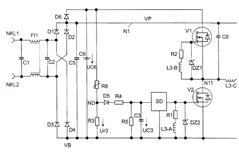
Illustrated on the left-hand side are two system supply
terminals NKL1 and NKL2, at which a system supply can be
connected to the electronic ballast. A filter comprising two
capacitors C1 and C2 and two coupled coils, denoted by FI1,
connect the system supply terminals NKL1 and NKL2 to a full-
bridge rectifier comprising the diodes D1 to D4. The rectified
supply voltage is applied to an intermediate circuit capacitor
C6, which is illustrated to the right of the full-bridge
rectifier in the figure, via a pump switch diode D6 which is
connected to the cathode-side end of the full-bridge rectifier
D1 to D4. The voltage UC6 drops across the intermediate circuit
capacitor C6.
CA 02550365 2006-06-16 -
2005P05619 US - 9 -
At the anode-side output of the full-bridge rectifier, the
reference potential VB is applied. At the cathode-side output
of the full-bridge rectifier, at a connection node N1 between
the full-bridge rectifier and the pump switch diode D6, the
positive rectified supply voltage VP is applied. An
interference suppression capacitor C5 for the purpose of
reducing system current harmonics is connected in parallel with
the full-bridge rectifier D1 to D4.
The intermediate circuit capacitor C6 feeds a supply power to
the converter, which in this case is in the form of a half
bridge comprising two switching elements V1 and V2. The
switching elements V1 and V2 are in this case in the form of
MOSFETs. By means of opposite clocking, they produce an AC
potential at the connection node between them, their center tap
NM, said AC potential oscillating between the reference
potential VB and the supply potential UC6 of the intermediate
circuit capacitor.
A series circuit comprising a lamp inductor L1, lamp terminals
KL1 and KL2 and a coupling capacitor C4 is connected between
the center tap NM and the reference potential VB. A discharge
lamp LA is connected to the lamp terminals KL1 and KL2.
A transformer coil L3-C is connected in series with the center
tap NM. A series circuit comprising a resistor R2 and a
transformer coil L3-B is connected between the center tap NM of
the converter and the gate of the switching element V1 on the
supply-potential side. A corresponding series circuit
comprising a resistor R1 and a transformer coil L3-A is
connected between the reference potential VB and the gate of
the switching element V2. A zener diode DZ1 or DZ2 for the
overvoltage protection of the switching element V1 or the
switching element V2 is connected in each case in parallel with
these series circuits comprising one of the resistors R2 and R1
and one of the transformer coils L3-B and L3-A, respectively.
The three transformer coils L3-A, L3-B and L3-C are
CA 02550365 2006-06-16-
2005P05619 US - 10 -
transformer-coupled to one another and symbolically represent a
self-excited controller for the switching times of the
switching elements V1 and V2.
A pump capacitor C9 is connected between the node N1 and the
left-hand lamp terminal KL1. A trapezoidal capacitor C8 is
connected in parallel with this pump capacitor, but to the
center tap NM. The trapezoidal capacitor C8 influences the
switching response over time of the switching elements V1 and
V2 and thus reduces switching losses. In this case, the
capacitors C8 and C9 are denoted, together with the lamp
inductor L1, as the pump network. The pump network C8, C9, L1
forms a pump branch together with the pump switch diode D6.
However, virtually any desired pump network topologies are
conceivable. It is critical that the pump network contains at
least one energy store, which is connected to the intermediate
circuit capacitor C6 via a pump switch.
A series circuit comprising a varistor R8 and a measuring
resistor R3 is connected in parallel with the intermediate
circuit capacitor C6. A node ND is located between the varistor
R8 and the measuring resistor R3. A delay circuit comprising a
diode D5, an integration resistor R4, a discharge resistor R5
and an integration capacitor C3 is connected between the node
ND and the reference potential VB. In this case, the diode D5
is connected in series with the integration resistor R4 and the
integration capacitor C3. The discharge resistor R5 is
connected in parallel with the integration capacitor C3. A
shutdown device SD is connected to the connection node between
the integration resistor R4 and the integration capacitor C3
via a highly resistive input. A deactivation output of the
shutdown device SD is connected to a control input of the
switching element V2.
During normal operation, when the discharge lamp LA is
connected and the gas discharge has been ignited, the pump
circuit functions as follows: the center tap NM of the
CA 02550365 2006-06-16 -..
2005P05619 US - 11 -
converter oscillates at a high frequency between the reference
potential VB and the supply potential UC6 of the intermediate
circuit capacitor C6. The coupling capacitor C4 is designed
such that the potential NH at the lamp terminal KL2 on the
reference-potential side corresponds to approximately half the
voltage UC6 across the intermediate circuit capacitor C6.
Driven by the oscillating potential at the center tap NM,
firstly the discharge lamp LA is operated and secondly charge
is pumped via the pump switch diode D6 into the intermediate
circuit capacitor C6 via the pump network comprising the
capacitors C8 and C9 and the lamp inductor L1.
In the event of coldstarting of a discharge lamp LA, the
following takes place in a circuit arrangement as shown in
figure 1: charge is pumped into the intermediate circuit
capacitbr via the pump switch diode D6 by means of the pump
network C8, C9 and L1. The more switching operations the
converter carries out prior to the gas discharge being ignited
in the discharge lamp LA, the greater the increase in the
voltage UC6 across the intermediate circuit capacitor C6.
The gas discharge in the discharge lamp LA is normally ignited
within a time interval in which the voltage UC6 across the
intermediate circuit capacitor C6 is not yet critical. If the
gas discharge does not ignite, the voltage UC6 acros s the
intermediate circuit capacitor C6 may reach such high values
that components in the electronic ballast, in particular the
intermediate circuit capacitor C6 itself, may be destroyed. The
circuit arrangement shown in figure 1 should reduce this risk.
If an overvoltage occurs at the capacitor C6, the otherwise
highly resistive varistor R8 assumes a low resistance value,
and a current flows through the series circuit comprising the
varistor R8 and the measuring resistor R3. In this case, the
varistor may dissipate high powers for a short period of time.
The voltage at which the varistor R8 assumes a low resistance
CA 02550365 2006-06-16
2005P05619 US - 12 -
value may vary severely from type to type, and also over the
life of such a varistor; 10% are not unusual in both cases.
The delay circuit which is connected in parallel with the
measuring resistor R3 detects the voltage UC3 across the
measuring resistor R3. In this case, the voltage is stored in
the integration capacitor C3. How rapidly the voltage UC3
across the integration capacitor C3 increases depends on the
dimensions of the components in the delay circuit. The charging
time constant is given by the nonreactive resistance of the
integration resistor R4 and the capacitance of the integration
capacitor C3. The discharge time constant is in this case given
by the capacitance of the integration capacitor C3 and the
nonreactive resistance of the discharge resistor R5. If the
discharge time constant is greater than the charging time
constant, the voltage UC3 across the integration capacitor C3
is proportional to the charge which has flowed through the
measuring resistor R3 since the connection of the varistor R8.
The charging time constant for the integration capacitor C3 is
set such that a current flow through the series circuit
comprising the varistor R8 and the measuring resistor R3 can be
maintained as long as is possible without the varistor R8 being
destroyed. The discharge lamp LA is thus given as long as
possible to ignite the gas discharge. If the voltage across the
integration capacitor C3 exceeds the switching threshold of the
shutdown device SD, the shutdown device SD deactivates the
switching element V2 of the converter. The voltage UC6 across
the intermediate circuit capacitor C6 therefore cannot rise any
further. The integration capacitor C3 is discharged via the
discharge resistor R5. This takes place slowly in comparison
with charging of the integration capacitor C3.
The shutdown device SD is a bistable shutdown device, i . a . it
is activated when a first switching threshold is exceeded and
thus the converter is deactivated, and activates the converter
when a second, smaller switching threshold is undershot. The
CA 02550365 2006-06-16
2005P05619 US - 13 -
discharge time constant for the discharge of the integration
capacitor C3 is set such that the converter is only reactivated
after a comparatively long period of time. The reason for this
is the fact that the varistor R8, when averaged over longer
intervals, cannot dissipate nearly as much power as during very
short intervals. A radiofrequency converter -
activation/deactivation cycle therefore needs to be prevented
such that the average power consumption over time of the
varistor does not exceed the corresponding limit value.
On the other hand, it is expedient to reactivate the converter
after a certain period of time since the event of the gas
discharge not being ignited may be an event which occurs only
once or since, in the meantime, the discharge lamp LA has been
replaced.