Note: Descriptions are shown in the official language in which they were submitted.
CA 02550486 2006-06-19
Printed Board Connector for Differential Signal Transmission
to Field of the Invention
The invention pertains to a printed board connector for producing direct
pluggable connections between printed boards, wherein said connector con-
sists of an insulating connector housing and disk-shaped modules that con-
Is tain electric contact elements and are arranged in the connector housing,
and wherein modules featuring signaling contacts and modules featuring
shielding contacts are alternately arranged adjacent to one another.
Backdround of the Invention
A printed board connector of this type is required for transmitting
differential
signal voltages from one printed board to another printed board by means of
a large number of electric contacts, wherein contacts that are shielded in
pairs are provided in order to ensure a low feedover between the line pairs.
Description of the related Art
US 6,506,076 discloses a rectangular connector, in which at least partially
angled shielding plates are positioned between a series of differential signal-
3o ing contacts that are arranged in rows and columns.
CA 02550486 2006-06-19
2
Summary of the Invention
The invention therefore is based on the objective of developing a printed
board connector of the initially cited type in such a way that a two-pole
signal
s conduction is respectively provided in order to transmit differential
signals,
wherein correspondingly designed shielding plates are provided between the
signal-conducting line pairs for shielding purposes.
This objective is attained in that two respective signaling contacts that form
a
differential pair are at least regionally separated by a shielding contact ar-
to ranged between the signaling pairs.
The printed board connector serves for connecting two printed boards that
are arranged at a right angle to one another. However, it would also be pos-
sible to realize a "straight" 180° connection referred to the printed
boards if
Is the terminal contacts are designed accordingly.
In order to preserve the advantages of a differential data transmission on the
path from the electronic components to the printed board or the backplane,
respectively, correspondingly designed high-capacity connectors are re-
2o quired that not only ensure a sufficient signal density, but also a high
signal
integrity.
Differential signals, in principle, are largely immune to common-mode inter-
ferences because the logic information is transmitted in the form of the volt-
2s age difference between the respective line pairs. However, it needs to be
ensured that the line pairs are shielded accordingly. In connectors designed
for this purpose, this is achieved by means of integrated and specially con-
structed shielding plates.
3o The advantages attained with the invention can be seen, in particular, in
that
the inventive printed board connector makes it possible to shield a plurality
of
differential signaling pairs that are arranged in a row from interfering
radiation
by inserting modules that feature a shielding plate in the form of a disk be-
CA 02550486 2006-06-19
3
tween the signaling modules that are respectively arranged adjacent to one
another in pairs and in which the signaling contacts are embedded. The
modules are preferably realized in the form of signaling and shielding mod-
ules that can be inserted into the connector housing adjacent to one another
s in a certain pattern, wherein two adjacently arranged signaling modules are
respectively separated by a shielding module.
According to one variation, this is achieved by inserting shielding modules in
the form of disk-shaped plates into the connector housing. In another varia-
Io tion, the shielding modules are realized in the form of modules that are
cov-
Bred with an insulating material.
In this case, it is advantageous that an angled terminal end pointing from the
shielding module to the printed board is respectively arranged between the
is two differential signaling contacts.
Two individual contacts that are arranged adjacent to one another in two
modules respectively form a differential signaling pair. Another differential
signaling pair is arranged opposite of this differential signaling pair. Conse-
2o quently, two adjacently arranged strip conductors form a differential
signaling
pair and are separated by another strip conductor for shielding purposes on
each side of the inserted printed board.
2s Brief Description of the Drawings
One embodiment of the invention is illustrated in the figures and described in
greater detail below. The figures show:
3o Fig. 1 is a perspective representation with a section through the interior
of a
printed board connector;
Fig. 2 is a perspective representation of the terminal side of the printed
board
connector;
CA 02550486 2006-06-19
4
Fig. 3 is a perspective representation of the terminal side of a modified
printed board connector;
Fig. 4 is a perspective representation of a signaling module;
Fig. 5a is a horizontal projection of detached signaling contacts;
s Fig. 5b is a horizontal projection of an insulating member;
Fig. 5c is a horizontal projection of the complete signaling module;
Fig. 5d is a top view of the narrow side of the signaling module;
Fig. 6a is a perspective representation of a shielding module;
Fig. 6b is a horizontal projection of the insulating member of the shielding
Io module;
Fig. 6c is a horizontal projection of a variation of the shielding module;
Fig. 7 is a perspective representation of two adjacently arranged signaling
modules;
Fig. 8 is a perspective representation of a signaling module situated adjacent
is to a shielding module;
Fig. 9 is a view of the bores in a printed board for the printed board connec-
tor, wherein the signaling and shielding modules are also schematically illus-
trated in this figure, and
Fig. 10 is a cross-sectional representation of the arrangement of the strip
2o conductors on a printed board.
Detailed Description of the Invention
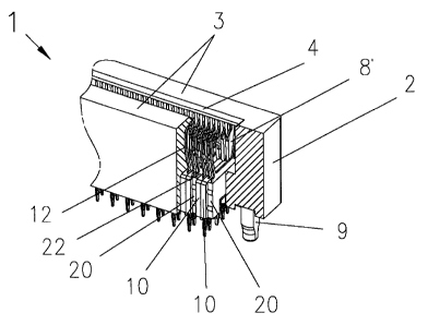
2s Figure 1 shows a perspective side view of a segment of a printed board con-
nector 1 with a partially sectioned region.
The printed board connector consists of a connector housing 2 with an inser-
tion slot 4 on the mating side for inserting a printed board between the disk-
3o shaped modules 10, 20 illustrated in the sectioned region, wherein said
modules are arranged in a certain sequence between the longitudinal sides 3
of the connector housing.
CA 02550486 2006-06-19
The plug contacts 12, 22 described further below are embedded in the disk-
shaped modules 10, 20 and respectively arranged in the connector housing
between chamber-forming walls 8' such that they are prevented from being
bent by the inserted printed board.
s
Figure 2 shows a perspective representation of a segment of the terminal
side of the connector housing 2, as well as the modules 10, 20 arranged
therein in the form of a row.
to In this case, two respective signaling modules 10 containing signaling con-
tacts 11 and a shielding module 20 with a shielding contact 21 embedded
therein are continuously arranged adjacent to one another.
This figure also shows a region in the connector housing 2, in which the
modules 10, 20 are removed so as to illustrate integral webs 5 that protrude
is into the housing interior from the two opposite longitudinal sides 3.
Two signaling modules 10 are respectively inserted into the horizontal inter-
mediate space 6 formed by the two webs 5.
The shielding modules 20 are inserted into the vertical clear space 7 be-
tween the webs 5.
2o In addition, a mounting post 9 is provided for holding the housing on a
corre-
sponding printed board in a mechanically stable fashion.
Figure 3 shows a variation of the connector housing 2, in which insertion
slots 8 are provided in both longitudinal sides 3 instead of the webs 5. In
this
2s case, the shielding modules 20' to be inserted into these insertion slots
are
merely realized in the form of a flat shielding plate 21 without a covering in-
sulating member.
In other respects, the arrangement of the signaling modules and the shield-
ing modules is identical to that shown in Figure 2. In this figure, the post
is
3o replaced with a bore 9' that serves for accommodating a not-shown external
mounting means.
CA 02550486 2006-06-19
6
Figure 4 shows a perspective representation of a signaling module 10. The
disk-shaped module consisting of a non-conductive insulating member 14
surrounds two electric signaling contacts 11 that are embedded independ-
ently of one another in this case, wherein these electric signaling contacts
s feature two springable plug contacts 12 that point toward one another, as
well as two terminal ends 13 that are realized in the fom~ of press-in
contacts
in this case.
In addition, the module contains a slot 18 on the side of the terminal ends 13
that is approximately arranged centrally referred to the insulating member,
to wherein the angled terminal end 23 of the adjacent shielding module 20 pro-
trudes into said slot when the connector is assembled.
Figures 5a-d show a variation of the signaling module 10 illustrated in
Figure 4.
Figure 5a shows the two signaling contacts 11 with the plug contacts 12 and
the terminal ends 13 that are realized in the form of soldering contacts in
this
case. In addition, a double bend 19 is provided such that the stretched shape
of the signaling contacts is preserved.
Figure 5b shows a variation of the insulating member 14, in which a button
16 and a recess 17 are respectively arranged alternately on the two periph-
eral surfaces of the insulating member in order to center the insulating mem-
bers relative to one another.
Figure 5c shows a complete signaling module.
Figure 5d shows a top view of the arrangement of the signaling contacts 11
within the insulating member 14 that is illustrated with broken lines in this
3o case, wherein this figure also shows that a bend 19 is provided--still
within
the insulating member--near the outlet region on the terminal end 13 such
that the signaling contact 11 extends asymmetrically referred to a central
CA 02550486 2006-06-19
position on the mating side and flush with the outer periphery 15 of the insu-
lating member 14 at the terminal end.
Figure 6 shows two variations of the shielding module 20 in the form of a
perspective representation.
Figure 6a shows the disk-shaped module 20 consisting of a non-conductive
insulating member 24, in which a flat, electrically conductive shielding con-
tact 21 is arranged.
to The mating side features two springable plug contacts 22 that point toward
one another while the terminal end 23 is bent out of the shielding contact 21
at a right angle.
Figure 6b shows an insulating member 24, in which a recess 28 for the an-
ts gled terminal end 23 is provided.
This figure also shows the segment-shaped press-on zones 26 that are re-
spectively moulded onto the opposing sides in pairs and ensure a secure
retention in the connector housing 2.
Figure 6c shows a variation of the shielding module 20, in which the insulat
2o ing cover of the insulating member 24 is omitted and the press-on zones 26
are directly moulded onto the flat shielding contact 21.
In this variation, the shielding module is inserted into corresponding slots 8
in
the longitudinal sides 3 of the connector housing.
2s modules 10 according to Figure 4, one of which is turned about its plug-in
axis by 180°.
If the modules are arranged tightly adjacent to one another, the plug contacts
12 are embedded symmetrically referred to the insulating member 14 and
arranged adjacent to one another in a uniformly spaced-apart fashion.
The plug contacts 12 are also arranged at a uniform height in order to con-
tact the strip conductors on the printed board.
CA 02550486 2006-06-19
The terminal ends 13, however, are arranged at different heights because
they respectively protrude from the insulating member in the first and in the
third quarter of the insulating member height and are respectively offset in
height by one quarter in the position with the 180° turn shown.
Consequently,
the terminal ends do not directly contact one another despite the directly ad-
jacent arrangement on the peripheral surfaces 15.
Figure 8 shows a signaling module 10 and a shielding module 20 that are
arranged adjacent to one another.
to This figure shows how the angled terminal end 23 is inserted into the slot
18
between the two terminal ends 13. In this respect, it should be noted that the
angled terminal end 13 of the shielding module extends into the slot 18 of
the next two adjacent signaling modules 10 and thusly exerts a shielding ef-
fect upon the two differential electric signals to both sides.
Is Due to the above-described contact arrangement, it is possible to offset
the
arrangement of the bores B (0.2 mm) on a printed board L by the material
thickness of the terminal ends 13 only such that a favorable routing of the
strip conductors on the printed board is achieved as shown in Figure 9.
This figure shows a view of the contours of the modules 10, 20 with the ter-
2o urinal ends 13 for the signaling contacts S1, S2, S3, S4 and 23 for the
ground connection G of the shielding contact, namely through a quasi-
transparent printed board L with the bores B.
Figure 10 shows a significantly enlarged representation of the arrangement
2s of the signaling strip conductors S and the shielding strip conductors G
(ground connection) on a printed board L. In this case, the strip conductors
S1 and S2 as well as the strip conductors S3 and S4 respectively form a dif-
ferential conductor pair above and underneath the printed board. A shielding
strip conductor G is respectively arranged adjacent thereto and followed by
3o another pair of signal conductors.