Note: Descriptions are shown in the official language in which they were submitted.
CA 02550502 2006-07-14
Title: Audio Amplifier
Field of the Invention
[1] This invention relates to amplifier circuits. More particularly, the
invention relates
to improved audio amplifier circuits.
Background of the Invention
[2] All sound reproduction systems employ some means for transducing
information
representing desired audio content into an audible sound field. Much effort
has been
made to improve the efficiency and to reduce the cost of such transducers.
Audio
amplifiers with modulated digital switching stages are known. However, these
amplifiers remain inefficient under various conditions, including when they
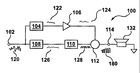
are called on
to reproduce audio signals of a small magnitude.
[3] Accordingly, it is desirable to provide a switching amplifier that
operates
efficiently and has a low cost. Furthermore, it is desirable to provide
speaker and
speaker assemblies that utilize the improved switching amplifier to provide an
improved
audio transducer.
Summary of the Invention
[4] In a first aspect, the present invention provides an audio amplifier that
includes
an input terminal for receiving an input audio signal, an output terminal, a
regulator
reference generator coupled to the input terminal, wherein the regulator
reference
generator provides a voltage regulator reference corresponding to the input
audio
signal; a voltage regulator coupled to the regulator reference generator,
wherein the
voltage regulator provides a power signal corresponding to the voltage
regulator
reference; a compensation block coupled to the input terminal to provide a
modulation
control signal based on the input signal; a modulator coupled to the
compensation block
wherein the modulator provides a modulated signal in response to the
modulation
control signal; and an output stage coupled to the modulator and the voltage
regulator,
wherein the output stage provides an output audio signal at the output
terminal by
combining the modulated signal and the power signal.
-1-
CA 02550502 2006-07-14
[5] In another, the invention provides an amplifier suitable for operation
using a
typical AC power source such as a municipal power source. In one embodiment,
an
active ground network is utilized to provide a balanced pair of power rails
about a
reference ground for a push-pull output stage. In another embodiment, the
power rails
are offset from a reference ground to reduce voltage stress on switches in a
push-pull
output stage.
[6] In another aspect aspect, the invention provides a multi-channel audio
signal
amplifier for amplifying two or more audio channels, wherein each channel
corresponds
to one input audio signal, the amplifier comprising: for each channel: (i) an
input
terminal for receiving an input audio signal for that channel; (ii) an output
terminal; (iii) a
compensation block coupled to the input terminal for the channel to provide a
modulation control signal for the channel; (iv) a modulator coupled to the
compensation
block for the channel to provide a modulated signal for the channel in
response to the
modulation control signal; and (v) an output stage; a regulator reference
generator
coupled to the input terminal for each channel, wherein the regulator
reference
generator provides a voltage regulator reference corresponding to the input
audio signal
having the largest magnitude; and a voltage regulator coupled to the regulator
reference
generator, wherein the voltage regulator provides a power signal corresponding
to the
voltage regulator reference, wherein the output stage for each channel is
coupled to the
modulator for that channel and the voltage regulator, wherein the output stage
for each
channel provides an output audio signal for the channel at the output terminal
for the
channel by combining the modulated signal for the channel and the power
signal.
[7] In another aspect, the invention provides a speaker comprising: electrical
elements that are electrically live when the speaker is in use, the electrical
elements
including a voice coil; moving elements that move in response to an audio
signal
received by the voice coil, wherein the moving elements include a diaphragm;
and an
isolation barrier mounted between the voice coil and the diaphragm.
[8] The electrical elements may also include an amplifier integrated into the
speaker.
The isolation barrier inhibits physical access to the electrical elements when
the
speaker is mounted in a typical speaker housing. The isolation barrier
includes a
central barrier typically positioned under the dust cap of a speaker, or
within a voice coil
-2-
CA 02550502 2006-07-14
former. The isolation barrier also includes a lateral barrier that is mounted
around the
voice coil former.
[9] In another embodiment, the isolation barrier includes a barrier flange
that
extends from the side of the speaker to inhibit access to the electrical
elements around
the side of the speaker.
[10] In other embodiments, the isolation barrier may also include a basket
barrier that
is integrated with or mounted to the basket of the speaker. The basket barrier
contains
apertures that are sufficiently small so as to prevent a finger or other
prohibited object
from contacting the electrical elements.
[11] In another embodiment, the isolation barrier includes a canister barrier
that
encloses all of the electrical elements of the speaker.
[12] A speaker according to these embodiments may be integrated into a speaker
assembly that includes an amplifier.
[13] These and other aspects of the invention are further identified and
elaborated on
in the course of describing various detailed embodiments below.
Brief Description of the Drawings
[14] A preferred embodiment of the present invention will now be described in
detail
with reference to the drawings, in which:
Figure 1 illustrates a first amplifier according to the present invention;
Figure 2 illustrates a second amplifier according to the present invention;
Figure 3 illustrates several exemplary signals in the amplifier of Figure 2;
Figure 4 illustrates a third amplifier according to the present invention;
Figure 5 illustrates a fourth amplifier according to the present invention;
Figure 6 illustrates several exemplary signals in the amplifier of Figure 5;
Figure 7 illustrates a fifth amplifier according to the present invention;
Figure 8 illustrates a sixth amplifier according to the present invention;
Figure 9 illustrates several signals of the amplifier of Figure 8;
Figure 10 illustrates a seventh amplifier according to the present invention;
Figure 11 illustrates several signals of the amplifier of Figure 10;
Figure 12 illustrates an eighth amplifier according to the present invention;
-3-
CA 02550502 2006-07-14
Figure 13 illustrates a ninth amplifier according to the present invention;
Figure 14 illustrates a tenth amplifier according to the present invention;
Figure 15 illustrates several signal of the amplifier of Figure 14;
Figure 16 illustrates an eleventh amplifier according to the present
invention;
Figure 17 illustrates a twelfth amplifier according to the present invention;
Figure 18 is a cross-sectional drawing illustrating a first speaker assembly
and a
first speaker according to the present invention;
Figure 19 is a cross-sectional drawing illustrating a second speaker assembly
and a second speaker according to the present invention;
Figure 20 is a cross-sectional drawing illustrating a third speaker assembly
and a
third speaker according to the present invention;
Figure 21 is a cross-sectional drawing illustrating a fourth speaker according
to
the present invention;
Figure 22 is a cross-sectional drawing illustrating a fifth speaker according
to the
present invention; and
Figure 23 is a cross-sectional drawing illustrating a sixth speaker according
to the
present invention.
[15] In the Figures, similar components of different embodiments of the
invention are
generally identified with similar reference numerals.
Detailed Description of Exemplary Embodiments
[16] Reference is first made to Figure 1, which illustrates a first audio
amplifier 100
according to the present invention. Amplifier 100 has an audio input terminal
102, a
reference generator 104, a voltage regulator 106, a compensation block 108, a
modulator 110, an output stage 112 and an audio output terminal 114.
[17] An input audio signal 120 is received at input terminal 102. The
particular
characteristics of input signal 120 will depend on the system in which the
amplifier is
implemented. In some systems, for example, input signal 120 may be a 1 volt
peak-to-
peak signal with a time-varying magnitude and a time-varying frequency.
[18] Reference generator 104 is coupled between input terminal 102 and voltage
regulator 106. Reference generator 104 is configured to process input signal
120 and
-4-
CA 02550502 2006-07-14
to provide a voltage regulator reference 122 corresponding to input 120. For
example,
reference generator 104 may be configured to apply a function f(n) to the
input signal
120 to generate the voltage regulator reference 122. In this first exemplary
embodiment, reference generator 104 applies a rectification, or absolute
value, function
to input signal 120. The voltage regulator reference 122 is a full-wave
voltage rectified
version of input signal 120.
[19] Voltage regulator 106 receives the voltage regulator control reference
122 and
provides a corresponding power signal 124. Voltage regulator 106 may be any
type of
voltage regulator that can receive a reference and generate one or more
voltage signals
in response.
[20] In an embodiment of the invention, the voltage regulator could be any
type of
regulator, such as a linear or switching power supply.
[21] Voltage regulator 106 will typically receive power from a power source
(not
illustrated in Figure 1). A skilled person will be able to select and
configure a suitable
voltage regulator 106.
[22] Forward compensation block 108 is coupled to input terminal 102 and
provides a
modulation control signal 126 corresponding to the input signal 120 and
corresponding
to the operation of reference generator 104. The operation of forward
compensation
block 108 is described in greater detail below.
[23] Modulator 110 receives the modulation control signal 126 and provides a
modulated signal 128 corresponding to the input audio signal 120. Modulator
110 may
be configured to provide a pulse width modulated signal, a pulse density
modulated
signal or another type of modulated signal 128.
[24] Output stage 112 receives the power signal 124 and the modulated signal
128
and combines them to provide an output audio signal 130 at output terminal
114.
Modulator 110 and output stage 112 have a complementary configuration and
operation.
[25] A load such as a speaker 132 will typically be coupled to the output
terminal 114,
when the amplifier is in use. Optionally, a filter (not shown) may be coupled
between
output terminal 114 and the speaker to smooth or reconstruct the output audio
signal
130 before it reaches speaker 132.
-5-
CA 02550502 2006-07-14
[26] Reference is next made to Figures 2 and 3. Figure 2 illustrates a second
amplifier 200 according to the present invention. Figure 3 illustrates several
exemplary
signals. Amplifier 200 receives an input signal 220 at input terminal 202.
Reference
generator 204 provides a voltage regulator reference 222. Power regulator 206
produces a pair of symmetric voltage signals: positive voltage signal 224+ and
negative
voltage signal 224- in response to the voltage regulator reference 222. The
positive and
negative voltage signals may also be referred to as positive and negative
voltage rails.
[27] Forward compensation block 208 operates analogously to forward
compensation
block 108 of amplifier 100 and provide a modulation control signal 226.
Modulation
control signal 226 preserves the sign of input signal but is otherwise of a
uniform
magnitude. At the bottom of Figure 3, a portion of signal 226 and a
corresponding
portion of modulated signal 228 and output signal 230 are illustrated.
Modulated signal
228 is a digital signal.
[28] Amplifier 200 has a push-pull output stage 212 that includes an inverter
240, a
gate drive block 244 and a pair of switches 246 and 248. Switch 246 is coupled
between the positive voltage signal 224+ and the output terminal 214. Switch
248 is
coupled between the negative voltage signal 224- and the output terminal 214.
Modulated signal 228 is coupled to gate drive block 244 in the original form
in which it is
generated by modulator 210 and in an inverted form through inverter 240. Gate
drive
block 244 operates switch 246 in response to the original form of modulated
signal 228
so that output terminal 214 is coupled to positive voltage signal 224+ when
modulated
signal 228 is high. Gate drive block 244 operates switch 248 in response to
the inverted
form of modulated signal 228 so that output terminal 214 is coupled to
negative voltage
signal 224- when modulated signal 228 is low. In an alternative embodiment,
only the
original form of modulated signal 228 may be provided to the gate drive block
and
inverter 244 may be integrated into the gate drive block.
[29] Output stage 212 generates the output audio signal 230 by coupling the
positive
voltage signal 224+ and the negative voltage signal 224- to the output
terminal 214 in
accordance with the modulated signal. Output audio signal 230 is a modulated
amplified version of the input signal 220 during the corresponding time
period.
-6-
CA 02550502 2006-07-14
[30] A speaker 232 may be coupled directly to the output terminal 214 or
alternatively,
a filter (not shown) may be coupled between the output terminal and the
speaker 232 to
smooth output audio signal 230.
[31] In an amplifier according to the present invention, the modulator,
voltage
regulator (or regulators when there is more than one, as illustrated below in
relation to
other embodiments) and the output stage are selected to operate together. In
amplifier
200, the push-pull output stage requires a positive voltage signal and a
negative voltage
signal, which are generated by voltage regulator 206. Switches 246 and 248 may
be
transistors and gate drive block 244 is selected to provide an appropriate
drive signal for
the switches. In this embodiment, modulated signal 228 may be a pulse density
modulated (PDM), pulse width modulated (PWM) or any other type of modulated
signal.
[32] Figure 4 illustrates a third amplifier 300 according to the present
invention. In
amplifier 300, the reference generator 304 and forward compensation block 308
operate
in the same manner as the corresponding components of amplifiers 100 and 200.
Voltage regulator 306 provides a power signal 324 at node 356.
[33] Amplifier 300 has a bridge output stage 312. Bridge output stage 312
includes
four switches 346, 348, 350 and 352 in a bridge configuration. A load 332 is
coupled
between a pair of output terminals 314a and 314b. Switch 346 is coupled
between
node 356 and output terminal 314a. Switch 348 is coupled between node 356 and
output terminal 314b. Switch 350 is coupled between output terminal 314a and
ground.
Switch 352 is coupled between output terminal 314b and ground.
[34] Modulator 310 provides a pair of digital modulated signals 328+ and 328-
that are
used to control switches 346 - 352. Modulated signal 328+ controls switches
346 and
352. Modulated signal 328- control switches 350 and 354.
[35] In this embodiment, modulated signals 328+ and 328- are symmetric in the
sense that when one of them is high, the other is low. In another embodiment
of an
amplifier with a bridge output stage, modulated signal 328+ and 328- may
provide a
trinary control, which is suitable for a class BD modulation scheme.
[36] When modulated signal 328+ is high, switches 346 and 352 are closed,
switches
348 and 350 are open and current flows from node 356 through switch 346,
output
terminal 314a, the load 332, output terminal 314b and switch 352 to ground.
When
-7-
CA 02550502 2006-07-14
modulated signal 328- is high, switches 346 and 352 are open, switches 348 and
350
are closed and current flows from node 356 through switch 348, terminal 314b,
load
332, terminal 314a and switch 350 to ground.
[37] Reference is next made to Figures 5 and 6. Figure 5 illustrates a fourth
amplifier
400 according to the present invention. Figure 6 illustrates several exemplary
signals
generated in amplifier 400. Components of amplifier 400 that correspond to
similar
elements of the amplifier described above are identified with similar
reference numerals.
Reference generator 404 receives input signal 420 and provides a voltage
regulator
reference 422. Reference generator 404 includes a rectifier 418 and a peak
detector
419 coupled between input terminal 402 and voltage regulator 406. Reference
generator 418 provides a rectified version 421 of input signal 420. Peak
detector 419
receives this rectified version of the input signal 420 and provides a voltage
regulator
reference 422 that corresponds to the envelope of input signal 420. Voltage
regulator
406 provides a power signal 424 corresponding to the envelope of the rectified
input
signal421.
[38] An optional delay block 416 is coupled between input terminal 402 and
feedback
compensation block 408. Delay block 416 provides a delayed input signal 423
that
tracks the input signal 420 but is delayed in time. Amplifier 400 utilizes a
feedback
compensation mechanism rather than the feed-forward compensation mechanism of
amplifiers 100, 200 and 300. Power signal 424 is coupled to feedback
compensation
block 408 through a scaler 407. Scaler 407 scales the power signal 424 to
provide a
scaled power signal 425. In the present embodiment, feedback compensation
block
408 is a divider. Feedback compensation block 408 generates a modulation
control
signal 426 equal to:
Delayed Input Signal 423
Modulation Control Signal 426 =
Scaled Power Signal 425 [39] In a practical embodiment of an amplifier
according to the present invention, as
the input signal 420 is processed through the rectifier 418, the peak detector
419 and
the voltage regulator 406, a delay will be introduced between the power signal
424 and
the input signal 420. Delay block 416 serves to the delay the input signal so
that the
delayed input signal 423 is synchronized (or is approximately synchronized) in
time with
-8-
CA 02550502 2006-07-14
the scaled power signal 425. The delay introduced by delay block 416 may also
take
into account any delay in scaler 407 and other relevant components of the
amplifier.
[40] In another embodiment of the invention, a phase shift block could be
coupled
between the input terminal 402 and the regulator generator 404. In this case,
delay
block 416 could be omitted. In another embodiment, a phase shift block could
be
coupled between the regulator reference generator 404 and voltage regulator
406.
[41] In another embodiment of the invention, scaler 407 may be coupled between
the
output of regulator reference generator 404 and compensation block 408.
[42] Figure 6 illustrates several exemplary signals in amplifier 400. The
signals are
not illustrated to scale. At the top of Figure 6, an exemplary input signal
420 is
illustrated. Voltage regulator reference 422 (not shown in Figure 6) generally
follows
the envelope of the rectified input signal 421 (not shown in Figure 6). The
peak detector
419 will have attack and release characteristics. These characteristics of the
peak
detector are discussed in greater detail below. The voltage regulator 406 will
have a
slew rate and regulation characteristics that limit the precision with which
the power
signal 424 tracks the voltage regulator reference 422.
[43] A corresponding scaled power signal 425 is also shown.
[44] The delayed input signal 423 corresponds to the input signal 420 and
tracks
slightly behind it. A skilled person will recognize that the delay period of
delay block 416
will not precisely synchronize the delayed input signal and the power signal
since the
delay in the power signal will depend on the characteristics of the rectifier
418, the peak
detector 419 and the voltage regulator 406. These characteristics may be
magnitude
and frequency dependent, with the result that different components of the
input signal
may be delayed differently.
[45] Modulation control signal 426 is generated by dividing the scaled power
signal
425 into the delayed input signal 423.
[46] The modulation control signal 426 serves two purposes.
[47] First, it preserves the sign of delayed input signal. If the amplifier
implements a
push-pull output stage (as illustrated in amplifier 200 (Figure 2)), then the
sign indicates
whether the output stage should be in a "push" configuration (with the
positive voltage
signal coupled to the output terminal) or in a "pull" configuration (with the
negative
-9-
CA 02550502 2006-07-14
voltage signal coupled to the output terminal). If the amplifier implements a
bridge
output stage (as illustrated in amplifier 300 (Figure 4)), then the sign
indicates the
direction in which current should flow through the load. A push-pull or bridge
output
stage may optionally be used with different amplifiers described herein.
[48] Second, the modulation control signal indicates the proportion of the
power
signal (or power signals when there are multiple power rails) that should be
coupled to
the output terminal. In a practical system according to the invention, the
power signal
will be generated to be larger than the magnitude of the desired output signal
430,
thereby providing some headroom in the output stage 412. For example, if the
input
signal has a magnitude of 0.65 volts and the desired output signal has a
magnitude of
volts, then the power signal may be generated with a magnitude of 25 volts.
The
modulated signal is generated so that the magnitude of the output signal will
be 20
volts, thereby providing for 5 volts or 20% of headroom between the power
signal and
the output signal. In effect, the duty cycle of the modulated signal is 80%.
This ratio of
15 80% may be considered a target ratio in an amplifier with these exemplary
characteristics. Other amplifiers according to the invention may have
different
headroom and duty cycle targets.
[49] The modulation block compares the scaled power signal with the magnitude
of
the delayed input signal. If the actual power signal is at the correct
magnitude to
20 provide the desired output signal (with the desired headroom), then the
modulated
control signal is generated so that the duty cycle of the modulated signal
will be at the
target ratio.
[50] However, if the power signal is at a lower magnitude than desired, then
the
magnitude of the modulated control signal is larger, thereby increasing the
duty cycle of
the modulated signal and compensating for the low level of the power signal.
Using the
example above, if the desired output signal level is 20 volts with a 20%
headroom, but
the power signal has a magnitude of only 23.5 volts, then the duty cycle of
the
modulated signal may be increased to 85.1 %, thereby providing an output
signal with a
magnitude of 20 volts. An example of this condition is illustrated in Figure 6
at 450.
The condition may arise because the peak detector or the voltage regulator (or
both)
does not attack quickly enough when the magnitude of the input signal rises.
-10-
CA 02550502 2006-07-14
[51] If the scaled power signal is at a lower magnitude than desired, the
magnitude of
the modulation control signal is smaller, thereby reducing the duty cycle of
the
modulated signal and compensating for the high level of the power signal.
Using the
above example again, if the desired output signal level is 16 volts with a 20%
headroom, but the power signal has a magnitude of 22 volts (rather than the
target
magnitude of 20 volts), then the duty cycle of the modulated signal may be
reduced to
72.7%, providing an output signal of 16 volts. This condition is illustrated
in Figure 6 at
452. The condition may arise if the peak detector releases slowly or the slew
rate of the
voltage regulator slows the decrease of the magnitude of the power signal,
thereby
holding the power signal at a higher level than is needed to generate the
output signal
with the desired magnitude.
[52] The attack and release characteristics of the peak detector are chosen
taking the
following criteria into account. The peak detector should preferably (although
not
necessarily) attack quickly enough to avoid a modulation index greater than 1,
which
would result in undesirable clipping of the output signal. The peak detector
should also
release slowly enough to reduce the appearance of undesired audio frequency
components in the power signal. In amplifier 400, the feedback compensation
mechanism provides some power supply rejection, reducing the effect of power
supply
inaccuracy and delay on the output signal. If the peak detector releases too
quickly, the
regulator reference may too closely follow the rectified input signal and the
power signal
will include audio frequency components. The feedback compensation mechanism
may
not be able to fully compensate for this, resulting in distortion in the
output signal.
[53] One of the advantages of the present invention is that the magnitude of
the
power signal tracks the magnitude of the output signal. This can allow the
headroom
between them to be less than in some prior art systems, thereby increasing the
power
efficiency of the amplifier. The peak detector should release sufficiently
quickly to
preserve this benefit of the invention.
[54] A power signal in a practical system may also have other characteristics
such as
a minimum magnitude or an offset voltage. The reference generator or the
voltage
regulator (or both) could be configured to implement these characteristics. An
amplifier
according to the present invention will be able to generate a modulation
control signal to
-11-
CA 02550502 2006-07-14
compensate for these characteristics. In a feed-forward compensation
configuration,
the compensation block may be programmed to compensate for such
characteristics.
In a feedback compensation configuration, the compensation block will
compensate for
such characteristics when comparing the scaled power signal with the delayed
input
signal to generate the modulation control signal.
[55] Amplifiers 100, 200, 300, 400 are illustrated with a single input
terminal and a
single output terminal. The present invention is also suitable for use with a
multi-
channel audio system. Reference is next made to Figure 7, which illustrates an
amplifier 500 according to the present invention. Amplifier 500 can amplify
five signals
or channels a-e. Amplifier 500 has five input terminals 502a - 502e at which
five input
signals 520a - 520e are received. (For clarity, only signals relating to
channel a are
illustrated.) Amplifier 500 has a rectifier 518 which full wave rectifies each
input signal
520 and also diode-ors the signals to provide a rectified signal 521 which, at
any time,
has a magnitude corresponding to the input signal 520 with the highest
magnitude. A
peak detector 519 provides a voltage regulator reference 522 corresponding to
the
envelope of rectified signal 521. Voltage regulator 506 provides an amplified
power
signal 524, which is coupled to an output stage 512 for each channel.
[56] For each channel, there is a delay block 516, feedback compensator 508,
modulator 510, an output stage 512 and an output terminal 514, which operate
on the
input signal for that channel in the same manner as describe above in relation
to
amplifier (Figure 5).
[57] Voltage regulator 506 generates a power signal with a sufficient
magnitude to
generate the output signal (524a to 524e) that is to have the highest
magnitude (and
which typically corresponds to the input signal with the highest magnitude).
The
remaining output signals will typically have a smaller magnitude
(corresponding to input
signal with a comparatively smaller magnitude). To facilitate this, the
feedback
compensation block 508 for each channel generates a modulation control signal
526
that reflects the desired magnitude and sign of the output signal 524 for that
channel.
The modulator 510 for each channel generates a modulated signal 528
corresponding
to the modulation control signal 526 for that channel. As described above in
relation to
amplifier 400, the modulation control signal 526 for each channel will direct
the
-12-
CA 02550502 2006-07-14
modulator 510 to produce a modulated signal 528 with an appropriate duty cycle
to
provide an output signal 530 for that channel with the desired magnitude.
[58] Amplifier 500 is one example of a multi-channel amplifier that may be
implemented with the present invention. The other amplifiers described above
and
be(ow may also be used to implement multi-channel amplifiers.
[59] Reference is next made to Figure 8, which illustrates another amplifier
600
according to the present invention. (In Figure 8 and in subsequent Figures,
various
signals that correspond to previously illustrated and described signals are
not illustrated
again.) Amplifier 600 includes a reference generator 604 and a voltage
regulator 606
which operate to produce a power signal 624. Reference generator 604 may be
constructed in the same manner as the reference generators of amplifiers 300
or 400.
Amplifier 600 includes a feedback compensation block 608 to generate a
modulation
control signal 626. Feedback compensation block 608 receives a delayed input
signal
623 and an output audio signal 630 and generates a modulation control signal
626
equal to:
Modulation Control Signal 626 = f (Delay Input Signal 623 - Output Signal
630)dt.
[60] Figure 9 illustrates an exemplary modulation control signal 626 and a
corresponding modulated signal 628. Modulator 610 generates a modulated signal
628
by comparing the modulation control signal 626 to a threshold, which may be
zero.
When the modulation control signal is greater than the threshold, the
modulator 610
generates a modulated signal 628 with a positive pulse. Conversely, when the
modulation control signal is less than the threshold, the modulator 610
generates a
modulated signal 628 with a negative pulse. The actual modulated signal
generated by
the modulator will depend on the modulation technique selected for the
amplifier.
In amplifier 600, the modulation control signal 626 is generated based on the
output
audio signal 630 rather than the power signal 628. This allows inaccuracies in
the
output audio signal 630 that may be introduced by output stage 612 through the
feedback compensation loop comprising feedback compensation block 608 to be
compensated for. Further, this implementation may be simpler to implement than
a
divider and no ramp is required in modulator 610.
-13-
CA 02550502 2006-07-14
[61] Reference is next made to Figure 10, which illustrates another amplifier
700
according to the present invention. Amplifier 700 also uses a feedback
compensation
mechanism to generate a modulated signal 728. A delayed input signal 723 is
generated by delay block 716. The output audio signal 730 is integrated
through an
integrator 732 to produce an integrated output signal 734. The integrated
output signal
is scaled through a scaler 736 to produce a scaled integrated output signal
738. The
scaling factor K of scaler 736 is selected to reduce the magnitude of the
integrated
output signal 734 to a magnitude suitable for comparison with the delayed
input signal
723. A summer 708 produces a modulation control signal 726 equal to:
Modulation Control Signal 726 = Delay Input Signal 723 - Kf Output Signal 730
dt.
[62] Modulator 710 is configured to compare the modulation control signal 726
to a
triangle wave 740 (or saw tooth wave) generated internally in the modulator.
When the
modulation control signal is higher than the triangle wave 740, a positive
pulse is
generated. When the modulation control signal is smaller than the triangle
wave 740, a
negative pulse is generated. As described above, the form of the modulated
signal 728
will be dictated by the modulation scheme that has been selected for the
particular
amplifier. The modulation control signal 726, triangle wave 740 and the
modulation
index of the modulated signal 728 are illustrated in Figure 11.
[63] Amplifier 700 includes a full wave rectifier 718 (not shown) and a peak
detector
719 (not shown) within reference generator 704 and a single power regulator
706. The
power regulator 706 may be configured to produce symmetric positive and
negative
power signals for use with a push-pull output stage (as is illustrated in
amplifier 200
(Figure 2)) or to produce a single power signal if the amplifier will include
a bridge
output stage (as is illustrated in amplifier 300 (Figure 4)).
[64] Reference is next made to Figure 12, which illustrates an amplifier 800
according
to the invention in which separate positive and negative power signals are
produced for
use with a push-pull output stage.
[65] Amplifier 800 includes two half wave rectifiers 804+ and 804-. Rectifier
804+ is
coupled between input terminal 802 and voltage regulator 806+. Rectifier 804+
half
wave rectifies an input signal 820 received at the input terminal 802 and
provides a
positive regulator reference 822+ corresponding to the positive half-waves of
input
-14-
CA 02550502 2006-07-14
signal 820. Rectifier 804- similarly produces a negative regulator reference
822-
corresponding to the negative half-waves of input signal 820 to voltage
regulator 806-.
[66] Voltage regulator 806+ produces a positive power signal 824+ that is
coupled to
output terminal 814 through switch 846. Positive power signal 824+ corresponds
to the
positive regulator reference 822+ and accordingly comprises a series of
positive going
half waves.
[67] Voltage regulator 806- similarly produces a negative power signal 824-
that is
coupled to output terminal 814 through switch 848. Negative power signal 824-
corresponds to the negative regulator reference 822- and accordingly comprises
a
series of negative going half waves.
[68] Delay block 816 and feedback compensation block 808 operate in the same
manner as the delay block 516 and feedback compensation block 508 of amplifier
500
(Figure 7). Modulator 810 generates a modulated signal 828 that is used to
control
switches 846 and 848 through a gate drive circuit 844, as described above in
relation to
amplifier 300 (Figure 4).
[69] Amplifiers 100 - 800 have been illustrated without details of the power
supply for
the voltage regulator.
[70] An amplifier according to the present invention may be implemented as
part of a
stand-alone speaker, such as a powered subwoofer. Reference is next made to
Figure
13, which illustrates an amplifier circuit 900 suitable for use in a stand-
alone speaker.
[71] Amplifier 900 receives an input signal 920 at an input terminal 902. A
safety
isolation block 903 is coupled between input terminal 902 and a node 905. The
safety
isolation block 903 provides physical isolation between input terminal 902 and
node
905. The safety isolation may be provided in safety isolation block 903 using
optical
isolation, RF isolation, an isolation transformer or any other technique for
physically
isolating two nodes in an electrical circuit. Safety isolation block 903
provides an
isolated input signal (not shown) at node 905.
[72] The isolated input signal is received by a voltage regulator reference
generator
904, which provides a voltage regulator reference 922 to voltage regulator
906. Voltage
regulator 906 receives power from a DC power supply 955. DC power supply 955
may
be plugged into a typical AC municipal power source (or another AC power
source)
-15-
CA 02550502 2006-07-14
through a plug 954. DC power supply 955 rectifies the AC power signal provided
by the
AC power source and provides a DC rectified power supply to the voltage
regulator 906
across nodes 956 and 957. Voltage regulator 906 provides a power signal 924 at
node
958 in response to reference 922. When measured across nodes 958 and 957, the
power signal 924 has a magnitude of twice the desired magnitude for the output
signal
930 at output terminal 914 (plus any headroom and taking into account
characteristics
of a peak detector and voltage regulator).
[73] Delay block 916 is coupled between node 905 and a feedback compensation
block 908. A feedback compensation loop including an integrator 933, scaler
938 and
feedback compensation block 908 operate as described above in relation to
amplifier
700 (Figure 10) to provide a modulation control signal 926 to modulator 910.
Modulator
910 provides a modulated signal 928 in response to the modulation control
signal 926.
The modulated signal 928 is received by a push-pull output stage 912
comprising a gate
drive block 944 and a pair of switches 946 and 948. Gate drive block 944
operates
switch 946 in response to the original form of modulated signal 928 and
operates switch
948 in response to an inverted form of modulated signal 928, which is
generated
internally in the gate drive block.
[74] The push-pull output stage 912 provides the output signal 930 at terminal
914. A
speaker 932 is coupled between terminal 914 and a reference node 959. Node 959
is
designated as a reference ground for amplifier 900, thereby effectively
splitting the
power signal 924 about the reference ground and allowing the output stage to
operate
in a push-pull configuration.
[75] Amplifier 900 also includes an active ground circuit 960. Active ground
circuit
includes a pair of resistors 961 and 962 of equal magnitude couple across
nodes 958
and 957. A summer 963 is coupled between the resistors at node 964. Resistors
961
and 962 split the power signal providing a reference center point for the
reference
ground at node 964. Summer 963 is also coupled to the reference ground at node
959
and provides an error signal equal to the difference between the voltages at
nodes 964
and the reference ground. A gate drive block 965 operates a pair of switches
in
response to the error signal, coupling either node 958 or node 957 to the
reference
ground at node 959, through a filter 968. Gate drive block 965 may be
implemented as
-16-
CA 02550502 2006-07-14
a saw-tooth or triangle wave generator and a comparator. The saw-tooth or
triangle
wave is centered about the reference ground. If the reference ground has a
voltage
higher than the reference point at node 964, then the reference ground is
pulled toward
the lower voltage at node 957 by closing switch 967. Conversely, if the
reference
ground has a voltage lower than the reference point at node 964, the reference
ground
voltage is increased by closing switch 966. Through this process, the active
ground
circuit 960 actively maintains the reference ground centered between the
voltages at
nodes 958 and 957.
[76] In an amplifier with a push-pull output stage, such as output stage 912,
only one
switch (switch 946 or 948) is closed at any point in time and only one power
rail (at
either node 958 or node 957) is connected to the load (speaker 932). The power
rail
that is not connected to the load may climb in magnitude due to charge
pumping. The
active ground circuit 960 mitigates this effect. The reference ground is not
fixed but
moves to be centered between the positive and negative voltage rails. By
forcing an
equal split between the two rails, the charge pumping current is effectively
cancelled.
[77] Reference is next made to Figure 14, which illustrates another amplifier
1000
according to the present invention that may be powered from an external AC
power
source.
[78] Amplifier 1000 does not have an active ground circuit. Instead switch
1066 is
switched together with switch 1048. Switch 1067 is switched together with
switch 1046.
This has the effect of offsetting the reference ground at node 1059, as
follows. In
Figure 14, gate drive block 1044 is illustrated as being directly coupled to
switches 1066
and 1067. In an alternative embodiment, a separate gate drive block may be
provided
for switches 1066 and 1067. The separate gate drive block could be driven by
the
outputs of gate drive block 1044 or by the modulated signal 1028 produced by
modulator 1010.
[79] Reference is also made to Figure 15, which illustrates this offsetting
effect.
Figure 15 illustrates the voltage V1058 at node 1058, the voltage V1057 at
node 1057, the
magnitude of the output signal 1030 measured at output terminal 1014 and the
magnitude of the input signal 1020 measured at input terminal 1002. Each of
these
signals is measured relative to the reference ground at node 1059.
-17-
CA 02550502 2006-07-14
[80] To generate a positive going output signal, as shown during time period
1070,
the output terminal 1014 is coupled to power signal 1024 at node 1058 for more
time
than the output terminal 1014 is coupled to node 1057. This is done by closing
switch
1046 for more time than switch 1048. When switch 1046 is closed, switch 1067
is also
closed. Closing switch 1067 has the effect of reducing the voltage across
capacitor
1072. On Figure 15, this is illustrated by V1057 rising towards the reference
ground on
node 1059. At the same time, the voltage across capacitor 1071 increases
(since the
potential between nodes 1058 and 1057 is determined by the magnitude of the
audio
output signal 1024). This is illustrated by V1058 rising relative to the
reference ground.
[81] Conversely, when switch 1048 is closed, switch 1066 is closed and switch
1067
is open. This is illustrated during time period 1073. The voltages at nodes
1058 and
1057 are offset to lower voltages relative to reference ground.
[82] By offsetting the voltages at nodes 1058 and 1057 in synchronization with
the
output signal 1030, the output signal can be generated with large voltage
swing, and a
correspondingly larger power output, than would be possible if voltage at
nodes 1058
and 1057 were symmetrical about the reference ground at node 1059. Typically,
switches 1046 and 1048 will be implemented as power transistors.
[83] Amplifier 1000 also mitigates the problem of charge pumping and also
reduces
the voltage stress on transistors 1046, 1048, 1066 and 1067 by up to a factor
of 2.
[84] Other control schemes may be used to control the operation of switches
1066
and 1067 to offset the voltages at nodes 1058 and 1057.
[85] Reference is next made to Figure 16, which illustrates another amplifier
1100
according to the present invention. Amplifier 1100 has a push-pull output
stage 1112
and uses the feedback compensation scheme described above in relation to
amplifier
400 (Figure 5). Amplifier 1100 has a voltage regulator 1106 that receives an
AC power
signal from an AC power source at a plug 1154. The AC power is rectified
through a
rectifier 1155 to provide a DC power signal. A switch 1181 receives the DC
power
signal and provides a regulated DC power signal to a transformer 1182.
Transformer
1182 has a split secondary winding and provides a positive voltage rail 1183+
through a
positive going half wave rectifier 1184+ and a switch 1185t.. Transformer 1183
also
provides a negative voltage rail 1183_ through a negative going half wave
rectifier 1184_
-18-
CA 02550502 2006-07-14
and a switch 1185_. The positive voltage rail 1183+ and negative volt rail
1183_ are
coupled through a pair of filtering capacitors 1190+ and 1190_.
[86] The voltages of rails 1183+ and 1183_ is regulated through a feedback
loop. The
negative voltage rail is inverted through an inverter 1186 and the inverted
negative rail
is diode-or'd with the positive rail by diodes 1187 and 1188. The lower of the
two rails is
compared to the regulator reference 1122 generated by regulator reference
generator
1104 to provide a voltage rail error signal 1189. The voltage rail error
signal 1189 is
used to control switch 1181, thereby regulating the voltage on rails 1183+ and
1181.
The error signal may be passed through an opto-coupler or RF coupler (not
shown) to
provide physical isolation of the input terminal and output terminal from the
plug 1154.
Alternatively, gate control signals generated from the error signal could be
coupled to
the switch 1181 through an isolation mechanism.
[87] In use, only one of the positive voltage rail 1183+ or the negative
voltage rail
1183_ will be coupled to the output terminal 1114 and the load 1132. The
voltage on the
rail 1183 that is not loaded will tend to rise as the corresponding capacitor
1190 become
charged due to non-ideal characteristics of the power circuit, such as the
leaking
inductance in the transformer, DC resistance of the transformer and other
factors.
Switches 1185 are used to address this. The positive voltage rail 1183+ is
coupled to a
comparator 1191+ that compares the voltage on the positive voltage rail 1183+
to a
maximum voltage Vmax+. If the voltage on the positive voltage rail exceeds the
maximum voltage, the comparator opens switch 1185, stopping the current flow
to
capacitor 1190+ and limiting the voltage on the positive voltage rail to
Vmax+. The
voltage on the negative voltage rail 1183_ is similarly limited to a minimum
voltage
Vmax_ through comparator 1191_.
[88] By limiting the voltage on the rail that is not coupled to the load,
amplifier 1100
allows a single point of control at the primary side of transformer 1181 to be
used to
regulate the voltage on both the positive and negative voltage rails.
[89] The voltages on the positive and negative voltage rails may also be
limited using
other techniques. For example, a voltage clamp may be coupled to between each
voltage rail and ground; a cross regulator may be used to transfer current
from one rail
to the other or a linear or post regulator may be inserted between each
voltage rail and
-19-
CA 02550502 2006-07-14
the output stage 1112 to limit the voltage on the rails. Also, the active
ground circuit
960 (Figure 13) could be used for the same purpose. These alternatives also
permit a
an inductor to be coupled in each of the voltage rails between the respective
rectifiers
1184 and the capacitor 1190, which may be desirable in some voltage regulation
schemes.
[90] Reference is next made to Figure 17, which illustrates another amplifier
1200
according to the present invention. The voltage regulator of amplifier 1100
may be used
with other types of amplifiers. Amplifier 1200 includes a voltage regulator
1206 that is
identical to voltage regulator 1106 and accordingly is not illustrated in
detail. The
voltage regulator 1206 is used to power a linear amplifier 1212. Amplifier
1212 includes
an analog drive stage 1292 and an output stage 1293 comprising a pair of
transistors
1294 and 1295. Analog driver stage 1292 receives the delay input signal from
delay
block 1216 and drives the transistors in response to it. Amplifier 1200 does
not include
a compensation block.
[91] Reference is next made to Figure 18, which illustrates a speaker assembly
1300
that includes amplifier 900 (Figure 13). Speaker assembly 1300 includes a
speaker 932
coupled across output terminal 914 and reference ground 959. The input
terminal 902
of amplifier is mounted on the housing 1302 of speaker assembly 1300. Plug 954
is
also illustrated and is coupled to the rest of amplifier 900 by a cord 1304.
The
remaining components of amplifier 900 are not separately illustrated.
[92] Speaker 932 includes a basket 1306 that is mounted to the speaker
assembly
housing 1302. The components of speaker 932 are mounted on the basket 1304.
Speaker 932 includes a platform 1308 on which a magnet 1310 is mounted.
Speaker
932 has a diaphragm 1312 and a dust cap 1314. Diaphragm 1312 is coupled to a
voice
coil former 1316 on which a voice coil is 1318 is wound. The ends of the voice
coil
terminate in voice coil leads 1320 and 1322. The voice coil leads are coupled
to output
terminal 914 and to node 959 to receive the output signal 930 (Figure 13)
produced by
amplifier 900. A spider 1324 supports moving components of speaker 932,
including
the diaphragm 1312, dust cap 1314, voice coil former 1316 and voice coil 1318.
Speaker 932 operates in conventional fashion in response to the output signal
930.
-20-
CA 02550502 2006-07-14
[93] As described above, safety isolation block 903 (Figure 9) physically
isolates the
input terminal 902 from the wall plug 954. This isolation is typically
required by
electrical safety authorities. Such authorities will also typically require
that a speaker
assembly must include a physical safety barrier that prevents physical access
from the
outside of speaker 932 to the voice coil 1316 and other electrically live
elements within
speaker assembly 1300. Figure 19 illustrates one method for doing so. A
barrier grill
1326 is installed on speaker housing 1302 to prevent physical access to the
interior of
speaker assembly 1300. Openings in barrier grill 1326 are made sufficiently
small that
fingers and other objects (which will typically be designated by electrically
safety
authorities) cannot reach the live electrical components inside speaker
assembly 1300.
[94] Reference is next made to Figure 19, which illustrates another speaker
assembly
1400 according to another aspect of the present invention. Speaker assembly
1400 is
also illustrated with amplifier 900. Speaker assembly 1400 includes a speaker
1405
that is made according to the present invention. Speaker assembly 1400 does
not
include a barrier grill. Instead, speaker assembly 1400 includes an isolation
barrier that
includes a central barrier 1430 and a lateral barrier 1432. The central
barrier 1430 is
mounted on platform 1408 beneath the dust cap 1414. The outer edge of the
central
barrier 1430 is adjacent the inside of the voice coil former 1416. The lateral
barrier
1432 surrounds voice coil former 1416. The space between the central barrier
and the
voice coil former and between the lateral barrier and the voice coil former is
preferably,
although not necessarily, smaller than is permitted under the standards set by
electrical
safety authorities. The lateral barrier 1432 is mounted to the basket 1406 at
the base of
the basket. Lateral barrier 1432 has a barrier flange 1436 that extends beyond
the base
of the basket 1406.
[95] In speaker 1405, the voice coil former is made of a non-conductive
material.
[96] The voice coil leads 1420 and 1422 are positioned beneath lateral
barrier. Voice
coil leads 1420 and 1422 are coupled to amplifier by wires 1440 and 1442. In
another
embodiment of a speaker according to the present invention, the voice coil
leads may
be integrated into spider 1424, which is also below the lateral barrier 1432.
Speaker
1405 includes a second optional spider 1450 that assists in supporting the
moving
components of the speaker.
-21-
CA 02550502 2006-07-14
[97] Speaker 1405 includes an optional EMI shield 1444. Other embodiments of
speakers according to the present invention may not include an EMI shield,
depending
on the application in which such a speaker will be used.
[98] The central barrier 1430 and the lateral barrier 1432 inhibit a finger or
other
object from punching through the dust cap or the diaphragm and touching the
voice coil
leads, voice coil or other live electrical elements of the speaker 1405 or the
speaker
assembly 1400.
[99] The barrier flange 1436 helps to inhibit a person from reaching through
the
basket and touching any live electrical element. The barrier flange is
optional and may
not be included in some speakers incorporating an isolation barrier according
to the
invention.
[100] Reference is next made to Figure 20, which illustrates another speaker
assembly
1500 and another speaker 1505 according to the present invention. Speaker 1500
does
not have an EMI shield. The isolation barrier of speaker 1500 includes a
central barrier
1530 and a lateral barrier 1432. However, the lateral barrier does not include
a barrier
flange. Speaker 1505 has a basket barrier 1552. Basket barrier 1552 may be
integrally
formed as part of the basket 1506 or may be mounted to the basket 1506. Basket
barrier 1552 contains apertures 1556 that permit air to travel through the
basket barrier
as diaphragm 1412 travels. However, the apertures 1556 are sufficiently small
that
fingers and other objects identified by safety authorities cannot reach
through basket
barrier to touch live electrical components inside speaker assembly 1500.
[101] Speaker assembly 1500 also incorporates an optional safety plug 1560. An
extension cord is used to provide electrical power to the safety plug 1560.
[102] Reference is next made to Figure 21, which illustrates another speaker
1605
according to the present invention. Speaker 1605 includes an isolation barrier
including
a central barrier 1630 and a lateral barrier 1632. The isolation barrier of
speaker 1605
also includes a canister barrier 1670 which extends around the base of speaker
1605.
All live electrical elements of speaker 1605 are enclosed by the isolation
barrier.
Speaker 1605 has a safety plug 1670 at which it receives electrical power.
Speaker
1605 also has an input terminal 1672 that is coupled to the input terminal 902
of the
amplifier 900 integrated within the speaker.
-22-
CA 02550502 2006-07-14
[103] Speakers assemblies 1400 and 1500 have been illustrated with amplifier
900.
These speaker assemblies may be used with any amplifier, including amplifiers
that are
not described herein to utilize the isolation barrier or the basket barrier or
both.
Furthermore, speakers 1400 and 1500 may be used with other amplifiers and
speaker
assemblies to provide the benefits of the isolation barrier or the basket
barrier or both.
Similarly, speaker 1605 may be used with another amplifier and with any
speaker
assembly. In each of the speakers 1400, 1500 and 1600 the isolation barrier
(or at least
part of the isolation barrier) is positioned between the voice coil and other
moving
elements of the speaker.
[104] Reference is next made to Figure 22, which illustrates a portion of a
speaker
1805 according to the present invention. A portion of the voice coil former
1816, voice
coil 1818, magnet 1810 and dust cap 1814 are illustrated. An inner insulator
1880
mounted inside the voice coil former 1816 and an outer insulator 1882 mounted
outside
the voice coil former are also illustrated. Inner insulator 1880 and outer
insulator 1882
are spaced apart from the voice coil former 1816. An insulator gap 1886 is
formed
between the inner and outer insulators. This gap is smaller than the thickness
1888 of
the voice coil, thereby inhibiting the voice coil from being pulled through
the insulator
gap. Speaker 1805 reduces the chance that a person will pull the voice coil of
the
speaker out of the speaker thereby exposing a potentially live voice coil.
[105] Reference is next made to Figure 23, which illustrates another speaker
1905
according to the present invention. Speaker 1905 is similar to speaker 1805
and also
includes a blocking collar 1890 mounted on the voice coil former. The blocking
collar is
preferably made of a non-conducting material. The thickness of blocking collar
1892 is
also greater than the insulator gap 1986. In speaker 1805, the voice coil
could
disintegrate and could be pulled through the insulation gap in pieces or in a
strand or
wire. Blocking collar 1892 helps to prevent this by providing an initial
barrier that will
inhibit the voice coil from reaching the insulator gap.
[106] The small insulator gap and blocking collar of speakers 1805 and 1905
may be
used with speaker 1400, 1500, 1600 and 1700 and with speakers that do not
incorporate an isolation barrier.
-23-
CA 02550502 2006-07-14
.
[107] The present invention has been described here by way of example only.
Various
modification and variations may be made to these exemplary embodiments without
departing from the spirit and scope of the invention, which is limited only by
the
appended claims.
-24-