Note: Descriptions are shown in the official language in which they were submitted.
CA 02550765 2006-06-20
WO 2005/102020 PCT/US2005/000498
Photonic Crystal Defect Cavity Biosensor
BACKGROUND OF THE 1NVENTION
A. Field of the Invention
This invention relates generally to photonic crystal biochemical sensor
devices. Such
devices are used for optical detection of the adsorption of a biological
material, such as DNA,
protein, viruses or cells, or chemicals, onto a surface of the device or
within a volume of the
device. More particularly, this invention is related to a biosensor having the
form of a
photonic crystal having defect cavities formed in a periodic pattern in the
device. The
invention provides a higher sensitivity and a greater degree of spatial
localization of
incoupled photons than previously reported photonic crystal biosensor devices.
B. Description of Related Art
Photonic Ciystals
Photonic crystals represent a new class of optical devices that have been
enabled by
recent advances in semiconductor fabrication tools with the ability to
accurately deposit and
etch materials with precision less than 100 nm. Photonic crystals are
characterized by an
infinite or semi-infinite periodic structure contaiining alternating materials
of low dielectric
permittivity and high dielectric permittivity. In principle, a photonic
crystal structure may
extend in 1, 2, or 3 dimensions of space. For background information on
photonic crystals,
the reader is directed to Joannopoulos, J.D., R.D. Meade, and J.N. Winn,
Photonic Crystals,
1995 Princeton, NJ: Princeton University Press.
Along with the development of appropriate fabrication methods, accurate
computer
modeling tools are also becoming available which facilitate design of
components with the
ability to manipulate the propagation of light within a photonic crystal
structure. Like the
periodic arrangement of atoms within a semiconductor crystal that results in
the formation of
energy bands which dictate the conduction properties of electrons, the
periodic arrangement
of macroscopic dielectric media within a photonic crystal is designed to
control the
propagation of electromagnetic waves. Because the period of the structure is
smaller than the
wavelengtli of light, such devices are often referred to as "sub-wavelength
surfaces" or as
"nanostructured surfaces" because typical dimensions are 50-300 nm. Using
photonic crystal
-1-
CA 02550765 2006-06-20
WO 2005/102020 PCT/US2005/000498
design principles, one may construct devices with optical energy bands, which
effectively
prevent the propagation of light in specified directions and energies, while
allowing
concentration of electromagnetic field intensity within desired volumes and
surfaces. See,
e.g., Munk, B.A., Frequency Selective Surfaces. Wiley Interscience. 2000: John
Wiley &
Sons; Pacradouni, V., W.J. Mandeville, A.R. Cowan, P. Paddon, J.F. Young, and
S.R.
Johnson, Plaotonic band structure of dielectric inenzbnanes periodically
textured in two
diinensions. Physical Review B, 2000. 62(7): p. 4204-4207.
The applications of photonic crystal structures within the field of
optoelectronics have
been numerous, including integration with lasers to inhibit or enhance
spontaneous emission,
waveguide angle steering devices, and narrowband optical filters. See e.g.
Quang, T., M.
Woldeyohannes, S. John, and G.S. Agarwal, Coherent control of spontaneous
emission.
Physical Review Letters, 1997. 79(26): p. 5238-5241 Liu, Z.S., S. Tibuleac, D.
Shin, P.P.
Young, and R. Magnusson, High efficiency guidecl-naode resonance filter.
Optics Letters,
1998. 23(19): p. 1556-1558; Peng, S., Experimental denzonstration of resonant
anoTnalies in
diffi~action froin two-dimensional gratings. Optics Letters, G. Michael
Morris. 21(8): p. 549-
551; Magnusson, R. and S.S. Wang, New principle for optical filters. Applied
Physics
Letters, 1992. 61(9): p. 1022-1024. Several device applications take advantage
of the
photonic crystal structure geometry's capability for concentrating light into
extremely small
volumes with very high local electromagnetic field intensity.
Defect cavity photonic crystals have been widely reported in the literature
for their
ability to enhance the Q and to spatially localize regions of high
electromagnetic field
intensity. John, S., Strong localization of photons in certain disordered
dielectric
superlattices. Physical Review Letters, 1987. 58(23): p. 2486-2489; Scherer,
A., T.
Yoshie, M. Loncar, J. Vuckovic, K. Okamoto, and D. Deppe, Photonic crystal
nanocavities
for efficient liglat con.fznemen.t and emission. Journal of the Korean
Physical Society, 2003.
42: p. 768-773; Srinvasan, K., P.E. Barclay, O. Painter, J. Chen, A.Y. Cho,
and C. Gmachi,
Experimental demonstf=ation. of a high quality factor photonic crystal
naicrocavity. Applied
Physics Letters, 2003. 83(10): p. 1915-1917; Painter, 0., K. Srinivasan, J.D.
O'Brien, A.
Scherer, and P.D. Dapkus, Tailoring of the resonant mode properties of optical
nanocavities
in two-diinensional photonic cfystal slab waveguides. Journal of Optics A:
Pure and Applied
Optics, 2001. 3: p. S161-S170 and John, S. and V.I. Rupasov, Multiphoton
localization and
-2-
CA 02550765 2006-06-20
WO 2005/102020 PCT/US2005/000498
propagating quantum gap solitons in a frequency gap medium. Physical Review
Letters,
1997. 79(5): p. 821-824. Periodic arrays of defect cavities in a photonic
crystal are reported
in Altug, H. and J. Vuckovic, Two-dinzensional coupled photonic cTystal
resonator arrays.
Applied Physics Letters, 2004. 84(2): p. 161-163.
Photonic Cfystal Biosensors
Several properties of photonic crystals make them ideal candidates for
application as
optical biosensors. First, the reflectance/transmittance behavior of a
photonic crystal can be
readily manipulated by the adsorption of biological material such as proteins,
DNA, cells,
virus particles, and bacteria. Each of these types of material has
demonstrated the ability to
alter the optical path length of light passing througll them by virtue of
their finite dielectric
permittivity. Second, the reflected/transmitted spectra of photonic crystals
can be extremely
narrow, enabling high-resolution determination of shifts in their optical
properties due to
biochemical binding while using simple illumination and detection apparatus.
Third,
photonic crystal structures can be designed to higlily localize
electromagnetic field
propagation, so that a single photonic crystal surface can be used to support,
in parallel, the
measurement of a large number of biochemical binding events without optical
interference
between neighboring regions within <3-5 microns. Finally, a wide range of
materials and
fabrication methods can be employed to build practical photonic, crystal
devices with high
surface/volume ratios, and the capability for concentrating the
electromagnetic field intensity
in regions in contact with a biochemical test sample. The materials and
fabrication methods
can be selected to optimize high-volume manufacturing using plastic-based
materials or high-
sensitivity performance using semiconductor materials.
Representative examples of biosensors in the prior art are disclosed in
Cunningham,
B.T., P. Li, B. Lin, and J. Pepper, Colorimetric resonant reflection as a
direct biochernical
assay technique. Sensors and Actuators B, 2002. 81: p. 316-328; Cunningham,
B.T., J. Qiu,
P. Li, J. Pepper, and B. Hugli, A plastic colorinietric resonant optical
biosensor for
multiparallel detection of label-free biochenaical interactions, Sensors and
Actuators B, 2002.
85: p. 219-226; Haes, A.J. and R.P.V. Duyne, A Nanoscale Optical Biosensor:
Sensitivity
and Selectivity of an 4ppf oach Based on the Localized Surface Plasinon
Resonance
Spectroscopy of Ti-iangular Silver Nanoparticles. Journal of the American
Chemical Society,
2002. 124: p. 10596-10604.
-3-
CA 02550765 2006-06-20
WO 2005/102020 PCT/US2005/000498
The combined advantages of photonic crystal biosensors may not be exceeded by
any
other label-free biosensor technique. The development of highly sensitive,
miniature, low
cost, highly parallel biosensors and simple, miniature, and rugged readout
instrumentation will
enable biosensors to be applied in the fields of pharmaceutical discovery,
diagnostic testing,
environmental testing, and food safety in applications that have not been
economically feasible
in the past.
In order to adapt a photonic bandgap device to perform as a biosensor, some
portion
of the structure must be in contact with a liquid test sample. Biomolecules,
cells, proteins, or
other substances are introduced to the portion of the photonic crystal and
adsorbed where the
locally confined electromagnetic field intensity is greatest. As a result, the
resonant coupling
of light into the crystal is modified, and the reflected/transmitted output
(i.e., peak
wavelength) is tuned, i.e., shifted. The amount of shift in the reflected
output is related to the
amount of substance present on the sensor. The sensors are used in conjunction
with an
illumination and detection instrument that directs polarized light into the
sensor and captures
the reflected or transmitted light. The reflected or transmitted light is fed
to a spectrometer
that measures the shift in the peak wavelength.
The ability of photonic crystals to provide high quality factor (Q) resonant
light
coupling, high electromagnetic energy density, and tight optical confinement
can also be
exploited to produce highly sensitive biochemical sensors. Here, Q is a
measure of the
sharpness of the peak wavelength at the resonant frequency. Photonic crystal
biosensors are
designed to allow a liquid test sample to penetrate the periodic lattice, and
to tune the
resonant optical coupling condition through modification of the surface
dielectric constant of
the crystal through the attachment of biomolecules or cells. Due to the high Q
of the
resonance, and the strong interaction of coupled electromagnetic fields witli
surface-bound
materials, several of the highest sensitivity biosensor devices reported are
derived from
photonic crystals. See the Cunningham et al. papers cited previously. Such
devices have
demonstrated the capability for detecting molecules with molecular weights
less than 200
Daltons (Da) with high signal-to-noise margins, and for detecting individual
cells. Because
resonantly-coupled light within a photonic crystal can be effectively
spatially confined, a
photonic crystal surface is capable of supporting large numbers of
simultaneous biochemical
assays in an array format, where neighboring regions within -10 m of each
other can be
-4-
CA 02550765 2006-06-20
WO 2005/102020 PCT/US2005/000498
measured independently. See Li, P., B. Lin, J. Gerstenmaier, and B.T.
Cunningham, A new
method for label-free imaging of biomoleculaf- interactions. Sensors and
Actuators B, 2003.
There are many practical benefits for biosensors based on photonic crystal
structures.
Direct detection of biochemical and cellular binding without the use of a
fluorophore,
radioligand or secondary reporter removes experimental uncertainty induced by
the effect of
the label on molecular conformation, blocking of active binding epitopes,
steric hindrance,
inaccessibility of the labeling site, or the inability to find an appropriate
label that functions
equivalently for all molecules in an experiment. Label-free detection methods
greatly
simplify the time and effort required for assay development, while removing
experimental
artifacts from quenching, shelf life, and background fluorescence. Compared to
other label-
free optical biosensors, photonic crystals are easily queried by simply
illuminating at normal
incidence with a broadband light source (such as a light bulb or LED) and
measuring shifts in
the reflected color. The simple excitation/readout scheme enables low cost,
miniature, robust
systems that are suitable for use in laboratory instruments as well as
portable handheld
systems for point-of-care medical diagnostics and environmental monitoring.
Because the
photonic crystal itself consumes no power, the devices are easily embedded
within a variety
of liquid or gas sampling systems, or deployed in the context of an optical
network where a
single illumination/detection base station can track the status of thousands
of sensors within a
building. While photonic crystal biosensors can be fabricated using a wide
variety of
materials and methods, high sensitivity structures have been demonstrated
using plastic-based
processes that can be performed on continuous sheets of film. Plastic-based
designs and
manufacturing methods will enable photonic crystal biosensors to be used in
applications
where low cost/assay is required, that have not been previously economically
feasible for
other optical biosensors.
The assignee of the present invention has developed a first generation
photonic crystal
biosensor and associated detection instrument. The sensor and detection
instrument are
described in the patent literature; see U.S. patent application publications
U.S. 2003/0027327;
2002/0127565, 2003/0059855 and 2003/0032039. Methods for detection of a shift
in the
resonant peak wavelength are taught in U.S. Patent application publication
2003/0077660.
The biosensor described in these references include 1- and 2-dimensional
periodic structured
surfaces produced on continuous sheets of plastic film. The crystal resonant
wavelength is
determined by measuring the peak reflectivity at normal incidence with a
spectrometer to
-5-
CA 02550765 2009-03-04
obtain a wavelength resolution of 0.5 picometer. The resulting mass detection
sensitivity of
<1 pg/mm2 (obtained without 3-dimensional hydrogel surface chemistry) has not
been
demonstrated by any other commercially available biosensor.
A fundamental advantage of first-generation photonic crystal biosensor devices
is
their ability to be mass-manufactured with plastic materials in continuous
processes at a 1-2
feet/minute rate. Methods of mass production of the sensors are disclosed in
U.S. Patent
application publication 2003/0017581. As shown in Figure 1, the periodic
surface structure
of a biosensor 10 is fabricated from a low refractive index material that is
overcoated with
a thin film of higher refractive index material 14. The low refractive index
material is
bonded to a substrate 16. The surface structure is replicated within the cured
epoxy 12
from a silicon-wafer "master" mold (i.e. a negative of the desired replicated
structure) using a
continuous-film process on a polyester substrate 16. The liquid epoxy conforms
to the
shape of the master grating, and is subsequently cured by exposure to
ultraviolet light. The
cured epoxy 12 preferentially adheres to the polyester substrate sheet 16, and
is peeled away
from the silicon wafer. Sensor fabrication was completed by sputter deposition
of 120 nm
titanium oxide (Ti02) high index of refraction material 14 on the cured epoxy
12 grating
surface. Following titanium oxide deposition, 3x5-inch microplate sections
were cut from the
sensor sheet, and attached to the bottoms of bottomless 96-well and 384-well
microtiter plates
with epoxy.
As shown in Figure 2, the wells 20 defining the wells of the mircotiter plate
contain a
liquid sample 22. The combination of the bottomless microplate and the
biosensor structure
10 is collectively shown as biosensor apparatus 26. Using this approach,
photonic crystal
sensors are mass produced on a square-yardage basis at very low cost.
The first-generation detection instrument for the photonic crystal biosensor
is simple,
inexpensive, low power, and robust. A schematic diagram of the system is shown
in Figure
2. In order to detect the reflected resonance, a white light source
illuminates a -1 mm
diameter region of the sensor surface through a 100 micrometer diameter fiber
optic 32 and a
collimating lens 34 at nominally normal incidence through the bottom of the
microplate. A
detection fiber 36 is bundled with the illumination fiber 32 for gathering
reflected light for
analysis with a spectrometer 38. A series of 8 illumination/detection heads 40
are arranged in
a linear fashion, so that reflection spectra are gathered from all 8 wells in
a microplate column
at once. See Figure 3. The microplate + biosensor 10 sits upon a X-Y
addressable motion
-6-
CA 02550765 2006-06-20
WO 2005/102020 PCT/US2005/000498
stage (not shown in Figure 2) so that each column of wells in the microplate
can be addressed
in sequence. The instrument measures all 96 wells in -15 seconds, limited by
the rate of the
motion stage. Further details on the construction of the system of Figures 2
and 3 are set
forth in the published U.S. Patent Application 2003/0059855.
SUMMARY OF THE INVENTION
The present invention provides further improvements and advancements to the
photonic crystal and colorimetric biosensors known in the prior art. Rather
than using a
regular repeating periodic structure to design a structured surface for a
photonic crystal
biosensor, as disclosed in the above-referenced patent application
publications, the present
invention provides for a photonic crystal biosensor in the form of an array of
unit cells.
Defects in the periodic structure of the sensor are introduced. The defects
are introduced
intentionally in the sensor design, typically one per unit cell, and consist
of regions where the
local dielectric permittivity is higher than the surrounding regions of the
surface structure.
The defects result in locally (around the defect) concentrated regions of high
electromagnetic
field density, compared to the regions away from the defect. The use of
defects within a
photonic crystal biosensor has not been previously reported.
More particularly, a defect cavity photonic crystal biosensor is provided
which
consists of an array of two-dimensional unit cells, each of the unit cells
having a substrate
and a multitude of raised portions arranged in a regular repeating pattern
wherein the raised
portions are separated from each other by adjacent void portions. The raised
portions are
made from a material having a relatively high index of refraction nl greater
than that of
water. Each of the unit cells further comprises comprise a defect wherein the
regular
repeating pattern of the raised portions separated by adjacent voids is
modified such that, at
the defect, the material having a relatively high index of refraction nl
occupies the space
which would otherwise been occupied by one or more of the voids. The defect is
such that a
localized maximum of electromagnetic field intensity is produced in the region
of the defect
in response to incident light on said photonic crystal at a resonant
frequency. During use, a
fluid containing a sample to be tested is placed on the photonic crystal and
contained in or
absorbed in the void portions surrounding the defect.
In preferred embodiments, a sample retaining structure is placed adjacent to
the array
having a plurality of openings in registry witli a plurality of the unit
cells, wherein a
-7-
CA 02550765 2006-06-20
WO 2005/102020 PCT/US2005/000498
biological or chemical sample may be introduced into the openings in the
structure and
adsorbed by the array proximate to the defect cavities of the unit cells. An
example of such a
sample retaining structure is the microtitre plates described previously.
The advantage over prior art biosensors without defect cavities as disclosed
herein is
potentially higher sensitivity, through higher interaction of the surface
electromagnetic field
and the test sample, better detection system resolution through more narrow
resonant peaks
that can be tracked with higher fidelity, and higher spatial resolution by
potentially limiting
incoupled photon lateral propagation distance to less than 3 microns.
This invention is a significant advance in the art because it allows for the
development
of label-free biosensor detection systems capable of detecting analytes with
lower molecular
weight, lower biochemical binding affinity, and lower concentration than would
otherwise be
possible. Sensors made in accordance with the illustrated embodiments provide
both
sharper resonant peaks (higher Q), and greater local concentration of
electromagnetic field
energy in the region of the defect cavities, which help produce a sensor with
greater
sensitivity. The higher sensitivity methods enabled by this invention are
highly desired in
commercial applications such as pharmaceutical screening, diagnostic tests,
and
environmental monitoring systems.
BRIEF DESCRIPTION OF THE DRAWINGS
Figure 1 is an illustration of a prior art biosensor arrangement.
Figure 2 is an illustration of a prior art biosensor and detection system for
illuminating
the biosensor and measuring shifts in the peak wavelength of reflected light
from the
biosensor.
Figure 3 is an illustration of an arrangement of 8 illumination heads that
read an
entire row of wells of a biosensor device comprising the structure of Figure 1
affixed to the
bottom of bottomless microtiter plate.
Figure 4A is a cross-section of a unit cell of a two dimensional prior art
photonic
crystal biosensor;
Figure 4B is a two-dimensional plot of electromagnetic field intensity in the
X and Y
directions for the unit cell of Figure 4A, obtained by using an FDTD computer
model of the
unit cell.
-8-
CA 02550765 2006-06-20
WO 2005/102020 PCT/US2005/000498
Figure 4C is a graph of the X component of the electromagnetic field intensity
for the
sensor of Figure 4A as a function of distance in the X direction, as
calculated by the FDTD
computer model at the top of the grating of the sensor, at the resonant
frequency.
Figure 4D is a graph of the X component of the electromagnetic field intensity
for the
sensor of Figure 4A as a function of the distance in the X direction, as
calculated by the
FDTD computer model at the bottom of the grating of the sensor, at the
resonant frequency.
Figure 4E is a graph of reflected intensity of electromagnetic field as a
function of
wavelength, showing the peak wavelength at n = 1.33 for material adjacent to
the biosensor
(simulating water present at the void regions of the biosensor), and at n=
1.34 for material
adjacent to the biosensor, with the graph clearly showing a shift to the right
at the peak
wavelength for n = 1.34.
Figure 5A is a cross-section of a unit cell of a two dimensional photonic
crystal
biosensor with a defect in the center of the unit cell;
Figure 5B is a two-dimensional plot of electromagnetic field intensity in the
X and Y
directions for the unit cell of Figure 5A, obtained by using an FDTD computer
model of the
unit cell.
Figure 5C is a graph of the X component of the electromagnetic field intensity
for the
sensor of Figure 5A as a function of distance in the X direction, as
calculated by the FDTD
computer model at the top of the grating of the sensor, at the resonant
frequency.
Figure 5D is a graph of the X component of the electromagnetic field intensity
for the
sensor of Figure 5A as a function of the distance in the X direction, as
calculated by the
FDTD computer model at the bottom of the grating of the sensor, at the
resonant frequency.
Figure 5E is a graph of reflected intensity of electromagnetic field as a
function of
wavelength, showing the peak wavelength at n = 1.33 for material adjacent to
the biosensor
(simulating water present at the void regions of the biosensor), and at n=
1.34 for material
adjacent to the biosensor, with the graph clearly showing a shift to the right
at the peak
wavelength for n = 1.34.
Figures 6A is a plan view of a unit cell of an alternative arrangement of a
defect cavity
photonic crystal biosensor.
Figure 6B is a two-dimensional plot of electromagnetic field intensity in the
X and Y
directions for the unit cell of Figure 6A, obtained by using an FDTD computer
model of the
unit cell.
-9-
CA 02550765 2006-06-20
WO 2005/102020 PCT/US2005/000498
Figures 6C and 6D are cross-sections of the unit cell of Figure 6A, taken
along the
lines 6C-6C and 6D-6D of Figure 6A.
Figure 7 is a plan view of an alternative embodiment of a defect cavity
photonic
crystal biosensor.
Figures 8-11 are various views of an instrument for illuminating the defect
cavity
photonic crystal biosensors and collecting the reflected light in order to
determine shifts in the
peak wavelength.
DETAILED DESCRIPTION OF THE PREFERRED EMBODIMENT
A photonic crystal biosensor is described herein which has defect cavities to
improve
the Q factor and sensitivity of the sensor. Examples of such biosensors will
be described
below in conjunction with the examples of Figures 5A, 6A and 7. The sensor is
formed as an
array of two-dimensional unit cells, each of the unit cells having a substrate
and a multitude
of raised portions arranged in a regular repeating pattern wherein the raised
portions are
separated from each other by adjacent void portions. The raised portions are
made from a
material having a relatively high index of refraction nl greater than that of
water. In one
possible embodiment the high index of refraction material 52 is sputter
deposited onto the
substrate pattern of raised portions 58 and adjacent void or low regions 59,
as shown in
Figure 5A.
Each of the unit cells includes a defect wherein the regular repeating pattern
of raised
portions separated by adjacent voids is modified such that, at the defect, the
material having a
relatively high index of refraction nl occupies the space of one or more of
the voids. This can
be seen for example in Figure 5A in which the defect 56 comprises a missing
void or low
region at the center of the unit cell (three consecutive raised portions in a
regular square
wave pattern of raised portions and adjacent void portions).
A localized maximum of electromagnetic field intensity is produced in the
region of
the defect in response to incident light on the photonic crystal at a resonant
frequency. This
property is shown in Figures 5B and 6B and discussed further below.
During use, a fluid containing a sample to be tested is placed on the photonic
crystal
and contained in the void portions in the space immediately above the surface
of the sensor.
A detection apparatus such as shown in Figures 2, 3 or 8 -11 detects the shift
in the peak
-10-
CA 02550765 2006-06-20
WO 2005/102020 PCT/US2005/000498
wavelength value at the resonant frequency due to the change in the index of
refraction in the
medium directly above the surface of the sensor. The shift in peak wavelength
value provides
information as to the contents of the sample due to the change in index of
refraction, as
reported in the literature cited in the background section.
Thus, in a principle aspect of this invention, resonant cavities within a
photonic
crystal lattice are formed from intentionally-introduced local defect regions,
where the
dielectric permittivity of the defect is higher than that of the surrounding
non-defect region.
Defect cavities may be introduced through the omission of a hole in a 2D
lattice (e.g., as
shown in Figure 5A), the omission of a line in a 1D lattice, or in a tapered
lattice duty cycle.
Figure 6A shows one possible embodiment of a defect 76 in the center of a
hexagonal
arrangement of holes 70 formed in a Si substrate, in which the holes at the
center is omitted,
and the holes 74 surrounding the center are smaller than those further away
from the center.
Other configurations for a defect cavity photonic crystal biosensor are of
course possible.
Optical microcavities are typically characterized by two key quantities, the
quality
factor (Q), a measure of the photon lifetime for the optical cavity mode
(computed as the
change in peak wavelength value divided by the full width of the peak at half
maximum), and
the modal volume (Veff), a measure of the spatial extent and energy density of
the mode.
While first-generation photonic crystal biosensors demonstrate Q-1000, and a
lateral photon
propagation distance of -3-5 m, defect cavity structures have been
demonstrated using
computer modeling with Q-40,000, and cavity confinement approaching the
theoretical limit
of one half wavelength. For a photonic crystal biosensor, an increase in Q
results in a
decreased width of the reflected resonance spectrum, which, in turn, results
in the ability to
resolve smaller shifts in the resonant wavelength. In addition, a limitation
of the photon
lateral propagation distance to -500 nm would enable -10x improved spatial
resolution for
binding images to be obtained. Iinproved spatial resolution can be used to
increase
microarray density to a scale where 10 m diameter microarray spots can be
effectively
imaged. The ability to measure binding from a 500x500nm spot, as enabled by
this invention,
also has important implications in that it leads directly to assay
miniaturization.
Micro/nanofluidic control systems are under development which will have the
capability for
dispensing reagents with sub-nanoliter volumes and sub-micrometer precision.
The use of
such control systems, combined with miniaturized assays, leads to the ability
to test or screen
-11-
CA 02550765 2006-06-20
WO 2005/102020 PCT/US2005/000498
a large number of samples in a short amount of time using the apparatus of
Figures 8-11 or a
modification thereof.
In order to take advantage of defect cavity structures for photonic crystal
biosensors, a
periodic array of defect cavities is preferably produced in an array that
covers an entire
biosensor surface (such as a bottomless 3x5-inch microplate or 1x3-inch
microarray bonded
to the surface of the sensor). Further information on periodic arrays of
defect cavities are
found in Altug, H. and J. Vuckovic, Two-dimensional coupled photonic cfystal
resonator
arrays. Applied Physics Letters, 2004. 84(2): p. 161-163 Finite-difference-
time-domain
(FDTD) computer modeling methods are preferably used to design and simulate
the defect
cavity structures in a biosensor. FDTD modeling has been shown to be an
effective
method for predicting resonant wavelength, resonant peak width, polarization
dependence,
Veff, and sensitivity.
Example and comparison to non-defect cavity biosensors
In the course of building, measuring, and computer modeling a guided mode
resonant
filter (GMRF) biosensor (an example of a 1-D surface photonic crystal), for
example one as
described in the prior published applications cited previously, the present
inventor came to
more fully understand the relationship between surface electromagnetic field
intensity and
sensitivity to surface adsorbed biological material. In particular, a finite-
difference time-
domain (FDTD) computer modeling method was used which enabled the
visualization of the
distribution of electromagnetic fields within any device structure, and the
deterniination of the
extent of lateral propagation of incoupled photons at the resonant wavelength.
Using Finite-Difference Time-Domain (FDTD) computer analysis, the performance
of
a photonic crystal biosensor structure without defects (PC) was compared with
a defect-cavity
photonic crystal (DCPC) biosensor. FDTD is an accurate method for determining
the
interaction of any physical structure with electromagnetic radiation. It
involves representing
the physical structure to be modeled as a 2 or 3-dimensional object consisting
of materials
with known dielectric permittivity. The physical structure is broken down into
a fine mesh of
volume elements, where each volume element is described by its individual
dielectric
properties. The physical structure can be illuminated with brief pulses of
light with any
origin, orientation, polarization, and intensity. FDTD solves Maxwell's
equations to
determine a nearly exact representation of how the light pulse propagates
through the physical
-12-
CA 02550765 2009-03-04
structure. Because the light pulse can be represented as a Fourier transform
of many separate
independent sinusoidal functions, FDTD can determine the frequency (or,
equivalently
wavelength) transmission/reflection characteristics of the physical structure.
FDTD can also
determine a spatial map of the electromagnetic field strength within and
around the physical
structure for any electromagnetic field component and any wavelength. For
physical
structures such as photonic crystals with periodically repeating patterns of
dielectric
permittivity in one or more directions, FDTD allows simulation of only a
single "unit cell" of
the structure with the application of periodic boundary conditions. The
results of a periodic
boundary condition simulation provide an accurate determination of the field
characteristics if
the unit cell is assumed to extend into infinity.
In this work, a commercially available software package (available from
Lumerical
Solutions, Inc. Suite 405 - 238 Alvin Narod Mews, Vancouver British Columbia,
Canada
V6B 5Z3) was run on a personal computer. First, a 1-dimensional linear
photonic crystal
biosensor of the design described in Gunningham, B.T., J. Qiu, P. Li, J.
Pepper, and B. Hugh,
A plastic colorimetric resonant optical biosensor for multiparallel detection
of label-free
biochemical interactions. Sensors and Actuators B, 2002. 85: p. 219-226 was
simulated.
Next, the same structure was simulated with a defect cavity introduced into
the stracture.
The structure of the PC without a defect is shown iri Figure 4A. It consists
of a
repeating pattern of raised regions and adjacent void or low regions in a
square wave
pattern. The low refractive index (n=1.5) dielectric material 50 with a linear
grating (square
wave) extending into the page (z-direction), and repeating into infinity in
the x-direction. The
surface stracture (raised portion 58) height is 170nm. The high and low
regions of the low
refractive index surface structure are covered with a 120nm-thick Ti02 high
refractive index
material 52 (n=2.25). The period of the structure is 500 nm, with equal width
high and low
regions. In the FDTD model, the unit cell 54, representing 15 periods of the
grating, is shown
by the box in Figure 4A. The unit cell encompasses some of the area above and
below the
grating stracture. The mesh of the structure is divided into 25 nm increments
in the x- and y-
dimensions. The region above the PC structure represents a water test sample
(n=1.33). The
structure is illuminated from below with an infinite (in the xz plane) TE
polarized 5 fsec 30 Gaussian pulse with an intensity of 1 V/m, essentially as
shown in Figure 2.
For the PC structure, FDTD determined that the frequency for resonant coupling
is
378.5 THz (790 nm wavelength). The spatial electromagnetic field distribution
of the E. field
-13-
CA 02550765 2006-06-20
WO 2005/102020 PCT/US2005/000498
component at the resonant wavelength is shown in Figure 4B. Due to the
periodic surface
structure, as expected, the field intensity follows a periodic pattern, with
highest field regions
on the upper structure surfaces, as shown in Figure 4C (the grating top
surface is defined as
the top of the square waves in Figure 4A). Figure 4D shows the field intensity
at the grating
bottom surface (at the base of the square waves in Figure 4A). The reflected
wavelength
spectrum is shown in Figure 4E (curve for n = 1.33). The interaction of the
sensor with the
test sample is determined by repeating the simulation, but with an increased
"water"
refractive index of n=1.34. The higher water refractive index results in a
shift of the resonant
peak to a higher wavelength. A shift coefficient (ShCoe) is defined as the
change in resonant
wavelength divided by the change in water refractive index (ShCoe = Okp/An). A
shift
coefficient of 125 is determined for this structure, and is consistent with
values measured for
actual PC sensors.
Next, a defect cavity photonic crystal (DCPC) structure was simulated. The
DCPC
structure was identical to the PC structure, except that one low region of the
square wave
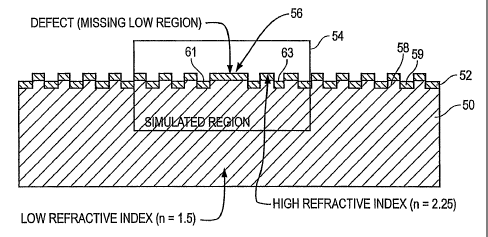
grating was replaced by a high region, as shown in Figure 5A at 56. Using the
unit cell
enclosed by the box 54, the defect is repeated every 7th period of the PC
grating, with the
defect approximately at the center of the unit cell. Because the defect
essentially displaces a
low refractive index material (water, n=1.33) which otherwise would have been
present at a
void in the center 56) with a higher refractive index material (n=1.5, i.e.,
the raised portion in
the substrate at the center 56, and n = 2.25, the high index of refraction
material deposited on
the raised portion at 56), the defect at 56 represents a region in the crystal
with a higher
refractive index than the regions surrounding the defect, e.g., at 61 and 63.
Using the same simulation conditions that were used with the PC structure of
Figure
4A, FDTD determined a resonant frequency of 334.2 THz (897 nm wavelength). A
higher
resonant wavelength is expected for the defect structure, as it has a higher
net dielectric
permittivity than the PC structure without the defect (Figure 4A), based on
the replacement
of water (n=l.33) with n=1.5 and n=2.25 material. The spatial electromagnetic
field
distribution of the E, field component at the resonant wavelength is shown in
Figure 5B. The
distribution shows that regions of the most intense electromagnetic field are
located near the
defect (spot 60), and lower peak field strength is obtained away from the
defect. As before,
the highest field intensity is obtained on the upper and lower exposed
surfaces of the structure
(grating top and bottom surfaces, as defined above), as shown in Figure 5C and
5D. The
-14-
CA 02550765 2006-06-20
WO 2005/102020 PCT/US2005/000498
reflectance spectrum for the sensor of Figure 5A for n=1.33 and n=1.34 in the
region directly
above the surface of the grating is show in Figure 5E. The shift coefficient
of the DCPC
structure of Figure 5A was found to be 134. A 7% improvement in sensitivity to
the "bulk"
refractive index of the test sample is obtained by the introduction of a small
defect as shown
in Figure 5A.
Other Exarnples of Defect Cavity Photonic Crystal Biosensors
Figures 6A is a plan view of a unit cell of an alternative arrangement of a
defect cavity
photonic crystal biosensor 10. The sensor 10 consists of a Si wafer substrate
72 having a
multitude of unit cells arranged in a two-dimensional array, one of which is
shown in Figure
6A. The unit cell includes a defect 76 at the center of the unit cell. The
pattern of raised
portions and adjacent void or low regions is formed by an arrangement of holes
70 etched in
the substrate 72, in which the hole which would otherwise be at the center 76
is omitted, and
the holes 74 surrounding the center 76 are smaller than those further away
from the center.
Figures 6C and 6D are cross-sections of the unit cell of Figure 6A, taken
along the liens 6C-
6C and 6D-6D of Figure 6A.
Figure 6B is a two-dimensional plot of electromagnetic field intensity in the
X and Y
directions for the unit cell of Figure 6A, obtained by using an FDTD computer
model of the
unit cell. A defect in a photonic crystal lattice (shown here as an array of
etched holes in a
silicon wafer) results in localized confinement of photons in the region
surrounding the
defect, resulting in higher resonator Q factor, and higher local
electromagnetic field intensity.
An array of unit cells 54 of Figure 6A with such defects on a photonic crystal
surface are as a
means for increasing resolution and sensitivity of photonic crystal
biosensors.
The array of unit cells of Figure 6A in preferred embodiments is bonded to the
bottom
of a inicroarray device which provides a means for containing a fluid sample
on the surface of
the sensor. The sample holding wells in the microarray has a structure,
preferably one of
rows and columns, and the detection instrument preferably has a plurality of
illumination and
detection heads to read each of the wells in parallel. It will be appreciated
that in some
embodiments, there will be many unit cells per well in microarray, depending
on the size of
the well and the size of the unit cells, but also that the wells and reading
and detection
instrument may be miniaturized such that there are only a few, or even one,
unit cell per
illumination and detection head. Also, it will be appreciated that the
illumination of any of
-15-
CA 02550765 2006-06-20
WO 2005/102020 PCT/US2005/000498
the defect cavity biosensor described herein could be from below (as shown in
Figure 2) or
from above, and that the illumination could from below the substrate and the
detection
apparatus could be positioned above the substrate, detecting the transmission
of light through
the sensor.
Figure 7 shows another embodiment in which the unit cell 54 of a photonic
crystal
consists of a two-dimensional checkerboard pattern in which a substrate
material (e.g., Si) has
a repeating patter of cubic etched holes 80 and adjacent cubic raised portions
82. The height
of the raised portions 82 (or, equivalently, the depth of the adjacent etched
holes) could be all
the same or they could have a tapered duty cycle wherein as the holes approach
the center 84
of the unit cell they are progressively shallower. The center portion 84
consists of portions of
the substrate in which the etched hole is omitted entirely, resulting in a
region of relatively
higher dielectric permittivity in the center region 84 than in the region
immediately
surrounding the center.
Other configurations for a defect cavity photonic crystal biosensor are of
course
possible. Detailed designs for other embodiments defect cavity photonic
crystal biosensors
are preferably arrived at using the FDTD techniques described herein.
Representative Detection Instrument
A representative detection instrument for illuminating a biosensor, detection
of
reflected radiation, and determining the peak wavelength at the resonant
frequency is shown
in Figures 8-11. The instrument of Figures 8-11 is specifically designed for
use with a sensor
affixed to the bottom of a bottomless microtiter plate of 8 columns of wells
and 12 rows. It
will be appreciated that modification of the instrument design, particularly
miniaturization of
critical system components, may be made for other embodiments.
The detection instrument 100 includes a plurality of dual illumination and
detection
fiber optic heads 40 (Figure 2) be arranged side by side in a linear fashion.
By utilizing such
a linear arrangement, a plurality of dual heads can simultaneously illuminate
and then read
out a plurality of sensor surface locations. For example, a linear probe
arrangement is utilized
in the instrument 100 to illuminate and then read an entire row or an entire
column of a
microtiter plate. In this preferred embodiment, each dual probe head contains
two optical
fibers. The first fiber is connected to a white light source to cast a small
spot of collimated
-16-
CA 02550765 2006-06-20
WO 2005/102020 PCT/US2005/000498
light on the sensor surface. The second fiber reflects the reflected radiation
and supplies it to a
spectrometer. After one row is illuminated, relative motion occurs between the
detector
probes and the sensor (microtiter plate) and the next row or column of the
sensor is read. The
process continues until all rows (or columns) have been read.
As will be described in further detail below, in one embodiment of the
measuring
apparatus, a biosensor comprising the combination of bottomless microtiter
plate and affixed
sensor grating is placed on a linear motion stage. The linear motion stage
moves the
microplate in a specified, linear scan direction. As the microtiter plate is
moved in this scan
direction, each microplate column is sequentially illuminated. The resulting
reflected light is
measured. In one preferred embodiment, a scan of a conventional 96-well
microtiter plate
may take approximately 15 to 30 seconds to illuminate and measure the
resultant reflected
spectrum.
In yet another alternative embodiment, an imaging apparatus utilizes a
spectrometer
unit that comprises an imaging spectrometer. One advantage of the imaging
spectrometer
system is that such imaging systems reduce the amount of time for determining
the peak
wavelength value (PWV). Another advantage is to study biological binding of an
area in a
non-uniform fashion. The use of an imaging spectrometer is described in
fiirther detail in
U.S. patent application publication 2003/0059855. The instrument includes a
spectrometer
unit preferably comprising an imaging spectrometer containing a two-
dimensional Charge
Coupled Device (CCD) camera and a diffraction grating. The reflected light
containing the
biosensor resonance signal for each spot is diffracted by the grating in the
spectrometer unit.
The diffraction produces a spatially segregated wavelength spectra for each
point within the
illuminated area. The wavelength spectrum has a second spatial component
corresponding to
the direction transverse to the scan direction. This second spatial component
is subdivided
into discrete portions corresponding to in this transverse direction.
For example, if the imaging spectrometer includes a CCD camera that contains
512 X
2048 imaging elements, then an illuminating line is spatially segregated into
512 imaging
elements or points. A wavelength spectra is measured for each of the 512
imaging elements
or points along the orthogonal axis of the CCD can7era. Where the CCD camera
contains 512
X 2048 imaging elements, the CCD would have a resolution of 2048 wavelength
data points.
Using this method, the PWV's of 512 points are determined for a single "line"
or imaging area
across the sensor bottom surface. For a conventional CCD imaging camera
typically having
-17-
CA 02550765 2009-03-04
spatial resolution of approximately 10 microns, a 1:1 imaging system is
capable of resolving
PWV values on sensor surface with a 10 micron resolution. In order to measure
a PWV
image of the entire sensor bottom surface, the sensor is transported along an
imaging plane
(scan direction), and subsequent line scans are used to construct a PWV image.
The embodiment of Figures 8-11 shows an illumination and detection instrument
that
incorporates the illumination and detection features of Figure 2 and 3. Figure
8 illustrates a
perspective view of the measuring instrument 100. The instrument 100 includes
a measuring
instrument cover 452 and a door 454. A microplate well plate (or microtiter
plate) 456
conFigured as a biosensor in accordance with this invention is shown in an
extracted position,
outside an incubator assembly 460 incorporated in the interior of instrument
100. The
microplate well plate 456 is held by a microwell tray 458. The tray 458 may
extend out of the
incubator assembly 460 through a door way 453 located at the front of the
incubator assembly
460. The incubator assembly 460 allows the tray 458 to be maintained at a user
defined
temperature during microwell tray read out and/or measurement.
In one preferred embodiment, the incubator assembly 460 is used for performing
assays at controlled temperatures, typically such controlled temperatures may
range from 4
and 45 degrees Celsius. As will be explained with reference to FIGS. 9-11, a
collimator
assembly 708 is positioned preferably beneath a bottom portion 602 of the
incubator assembly
460. During microtiter well illumination and wavelength measurement, the
collimator
assembly 708 illuminates a bottom surface 459 of the tray 458.
While the tray 458 remains in an extracted position outside of the incubator
assembly
460, the microtiter plate 456 may be placed on or removed from the tray 458.
The plate 456
may be held in the tray 458 via a set of registration points, spring clips, or
other known types
of securing means. In Figure 9, clips 457 are used to hold the plate 456 in
the tray 458.
After the microtiter plate 456 has been loaded with a fluid sample with
biological
material to be detected and measured, the tray 458 is transported into the
incubator assembly
460. Processing, mixing, heating, and/or readout of the biosensors may then
begin, preferably
under the control of a electronic microprocessor controller (not shown) on a
controller board
588 (see Figure 9).
Once the tray 458 retracts into the incubator assembly 460, the tray remains
stationary
during illumination and read out. For a readout of the microtiter plate 456 to
occur, the
collimator assembly 708 generates an illumination pattern that is incident
along the bottom
-18-
CA 02550765 2009-03-04
surface 459 of the plate 456. Preferably, the instrument 100 generates a beam
of light that is
incident along an entire row of wells of the plate 456.
Alterna.tively, the inst,rument 100 generates a plurality of illumination
beams that are
simultaneously incident on a plurality of plate wells. The illumination
pattern, comprising
multiple beams, is generated by dual illumination fiber optic probes contained
within the
collimator assembly 708. The construction of the probes is as shown in Figure
3. As
previously herein described, the light reflected off of the biosensor surface
may then be
detected by the same plurality of probes contained within a collimator
assembly 708. This
reflected light is then analyzed via the spectrometer system 590.
The incubator assembly 460 is provided with a plurality of apertures 764 along
a
bottom incubator assembly structure. As can be seen in Figure 11, incubator
assembly
apertures 764 are conFigured to generally line-up and match the well locations
657 on the
plate 456 when the plate 456 is in a readout position within the incubator
assembly 460. For
example, if there are 96 wells on the microwell well plate 456, the incubator
assembly bottom
portion 602 will be provided with 96 apertures 764. These apertures will be
configured in the
same type of array as the wells of the well plate (e.g., 8 rows by 12
columns). These apertures
764 provide clearance for light generated by collimator assembly 708 to reach
the wells from
the iIluminating probes 709.
To enable user access to the tray and to the plate, the plate tray 458 extends
out of the
measuring instrument 100. The tray 458 can be retracted into the instrument
100 and the door
454 closed to begin microplate processing. Such processing could include
mixing
liquid in the microtiter wells, heating deposited liquids to a predetermined
temperature,
illumination of the microplate 456, and processing various reflected
illumination patterns.
Figure 9 illustrates a perspective view 580 of various internal components of
the
instrament 100 illustrated in Figure 8. As shown in Figure 9, internal
components of the
measuring instrument 100 include a transition stage assembly 560, heater
controller unit 582,
a controller board assembly 588, and a spectrometer unit 590. The transition
stage assembly
560 includes the incubator assembly 460 and the collimator assembly 708. The
heater
controller unit 582, the controller board assembly 588, the transition stage
assembly 560, and
the spectrometer unit 590 are mounted on a base plate 592. The microplate well
tray 456 is
shown in the retracted position, outside of the incubator assembly 460.
-19-
CA 02550765 2009-03-04
The heater controller unit 582 provides temperature control to the incubator
assembly
460. The controller board assembly 588 provides functional controls for the
measuring
instrument including the mixing and other motion controls related to
translation stage 560 and
tray handling 458.
The spectrometer unit 590 contains an appropriate spectrometer for generating
the
PWV data. The design of the spectrometer will vary depending on the
illumination source.
Figure 10 illustrates a perspective view of the transition stage assembly 560
of the
measuring instrument 100 illustrated in FIGS. 8 and 9. Figure 11 illustrates
the transition
stage assembly 560 of Figure 10 with an incubator assembly top portion 461
removed (See
FIGS. 9 and 10). As can be seen from FIGS. 10 and 11, the transition stage
assembly 560
includes the microwell tray 458 positioned in the retracted position. The
microwell tray 458
has a plurality of wells 657, enters the incubation assembly 460 to initiate
the read out
process.
The microwell plate tray 458 is mounted on a top surface 605 of a bottom
portion 602
of the incubator assembly 460. Preferably, where the microtiter tray 456 is a
conventional
microtiter tray having 96 wells, the bottom portion 602 of the incubator
assembly 460
includes 96 holes. The microwell plate tray 458 is positioned over the bottom
portion of the
incubator assembly 602 such that the incubator assembly apparatus essentially
matches up
with the apertures (wells) contained in the microwell tray 458. Alternatively,
the bottom
portion 602 may contain a transparent section that matches the bottom portion
of the plate.
During specimen illumination and measurement, the microwell tray 458 is
preferably
held in a stationary manner within the incubator assembly 460 by the bottom
incubator
assembly portion 602. During illumination and measurement, the collimator
assembly 708 is
held in a stationary manner while a stepping motor 606 drives the incubator
assernbly,
including the plate, in a linear direction "A". As the incubator assembly 460
is driven along
direction "A," the collimator assembly 708 illuminates the bottom surface 459
of microtiter
plate 456. The resulting reflected illumination patterns are detected by the
collimator
assembly 708. A home position sensor 710 is provided as a portion of the
translation stage
assembly and to determine the position during the illumination process.
The transition stage assembly is provided with a plurality of elastomer
isolators
762. In this embodiment, a total of six elastomer isolators are used to
provide isolation and
noise reduction during illumination and read out.
- 20 -
CA 02550765 2006-06-20
WO 2005/102020 PCT/US2005/000498
As can be seen from FIGS. 10 and 11, the collimator assembly 708 is positioned
below a bottom surface 603 of the incubator portion bottom portion 602.
Preferably, the
collimator assembly 708 includes a plurality of dual fiber probe heads 709. In
the
embodiment illustrated in Figure 10, the collimator assembly 708 includes 8
dual fiber probe
heads 709. These dual fiber probes could have a probe head configuration
similar to the fiber
optic probes as previously described.
For ease of explanation, only the bottom plate 602 of the incubator assembly
460 is
shown is Figure 11. The incubator assembly bottom portion 602 is provided with
a plurality
of apertures 764. Preferably, where the microwell plate 456 is provided with
an 8 X 12 array
of wells such as illustrated in Figure 11, the incubator assembly bottom
portion 602 will also
include an 8 X 12 array of 96 apertures. These apertures will essentially
match the 96 wells on
the microwell plate 456. In this manner, the collimated white light generated
by the collimator
assembly 708 propagates through a first surface 603 along the incubator
assembly bottom
portion 602, and exit a second surface or top surface 605 of incubator
assembly bottom
portion 602. The collimated light can then illuminate a bottom well portion of
the microwell
plate 456. Alternately, bottom portion 602 may contain a transparent section
that matches the
bottom portion of the plate.
Referring to FIGS. 10 and 11, a drive motor 606 is provided for driving the
incubator
assembly during well scanning. A home position sensor 710 is provided as a
stop measuring
during the translation stage. The plate handling stage uses a stepping motor
702 to drive a
rack-and-pinion mechanism to move the tray in and out of the door to the
instrument. The
scanning stage uses a stepping motor 606 to drive a leadscrew 559 along
translation stage
rails 557, 558 to provide relative motion between the microwell plate 456 and
the
collimator assembly 708.
A mixer assembly may be used for mixing the liquid in the wells. In the
present
invention, a mixing mechanism is located between the incubation chamber of the
translation
stage. Additionally, a mixing mechanism may be provided in an alternative
location.
The grating surface of the sensor may be coated with compounds to enhance
binding
of target molecules in the sample, as described in the published application
of Pepper et al.,
U.S. Patent application 2003/0113766.
While presently preferred embodiments have been described with particularity,
persons skilled in the art will appreciate that modifications to the disclosed
embodiments are
-21-
CA 02550765 2006-06-20
WO 2005/102020 PCT/US2005/000498
contemplated as being within the scope of the invention. The scope is to be
determined by
reference to the appended claims.
- 22 -