Note: Descriptions are shown in the official language in which they were submitted.
CA 02551534 2006-07-04
- 1 - 2005P03137 US-rai
Circuit arrangement and method for operating at least one
electric lamp
Technical field
The present invention relates to a circuit arrangement for
operating at least one electric lamp having a drive circuit,
which has at least one terminal for a system voltage on the
input side and at least one terminal for the at least one
electric lamp on the output side, the drive circuit having a
control unit and a step-up converter having a step-up converter
inductor and a switch. It also relates to an operating method
for at least one electric lamp using such a circuit
arrangement.
Prior art
In such circuit arrangements in which the step-up converter is
used for system current harmonic correction (power factor
correction = PFC), the step-up converter is generally operated
in the so-called transition mode. In this case, transition mode
is understood to mean an operating mode in which the switching
operations of a switch in the step-up converter are carried out
at times at which the current through the step-up converter
inductor is equal to zero, i.e. the switch of the step-up
converter is closed, in the case of a falling edge of the
current through the step-up converter inductor, when the
current through the step-up converter inductor reaches the
value zero. If this step-up converter is operated using DC
voltage, this means that the step-up converter operates at a
fixed frequency and therefore the radio interference peaks at
the operating frequency which is established and their
harmonics are very narrow and very high, which entails a high
degree of complexity in terms of radio interference
suppression. In order to adhere to the predetermined radio
interference limit values, the radio interference filters
CA 02551534 2006-07-04
- 2 - 2005P03137 US-rai
therefore need to have sufficiently large dimensions and/or the
operating frequency needs to be selected to be so low that as
many harmonics as possible are in the range up to 150 kHz,
since in this range higher limit values apply in accordance
with the relevant standard. A further possibility for adhering
to the radio interference limit values consists in wobbling the
operating frequency of the step-up converter, which would,
however, lead to severe modulation of the current drawn from
the system (high RMS values). In addition, the possible
frequency modulation by means of wobbling is so low in
comparison to the bandwidth of the radio interference
measurement filters used in this case of the used radio
interference measuring devices that only a slight improvement
in the radio interference spectrum can be achieved. The
conventional bandwidth of such radio interference measurement
filters is 9 kHz at a transient response time of 1 s.
Figure 1 shows the time profile of the current through the
step-up converter inductor in the case of a known circuit
arrangement, which is operated in the transition mode. The
operating frequency is 105.0420 kHz, and the maximum amplitude
of the current is 40$ mA.
Summary of the invention
The object of th.e present invention therefore consists in
developing a circuit arrangement mentioned at the outset or an
operating method mentioned at the outset such that radio
interference suppression is made possible with little
complexity.
In principle, the invention is based on the concept of the
complexity involved with radio interference suppression being
low if the frequency spectrum is broadened using suitable
measures. According to the invention, this takes place by the
control unit being designed to operate the step-up converter in
CA 02551534 2006-07-04
- 3 - 2005P03137 US-rai
a discontinuous mcde, in which the current through the step-up
converter inductor has gaps, the duration of these gaps being
varied. Discontinuous mode is understood to mean an operating
mode in which, in contrast to the transition mode, the switch
is not closed again as early as at the time at which the
current through the step-up converter inductor reaches the
value zero, but there is a wait until a certain period of time
has elapsed, this period of time being varied. Even though the
current does not continuously remain at the value zero between
the time at which the value zero is reached and the time at
which the switch of the step-up converter is closed again as a
result of electrical reactions within the circuit arrangement,
this period of time is nevertheless referred to as a "current
gap", i.e. a currentless phase. By suitably selecting the
duration of the gaps, it is possible to achieve a bandwidth for
the operating frequency of the step-up converter which is far
greater than the bandwidth of the radio interference
measurement filter. Less radio interference therefore occurs in
the window of the predetermined bandwidth and this therefore
allows for lower interference levels which are therefore easier
to suppress. The larger the gap the lower the lowest frequency
of the resulting spectrum is. In contrast to the prior art, in
which a virtually discrete radio interference spectrum has
resulted, the radio interference spectrum of the invention has
been extended to a considerable extent. Owing to the change in
the duration of the gaps, in particular awing to the continuous
change in the duration of the gaps, it is thus possible for the
step-up converter to be operated over a wide frequency band.
Owing to the measure according to the invention, it is possible
to use higher operating frequencies, at which in principle it
is more difficult to suppress the interference, and therefore
smaller physical shapes for the step-up converter inductor can
be used and, as a result, cost savings can be achieved.
Switchover from the transition mode to the discontinuous mode
preferably takes place if the system voltage is a DC voltage.
CA 02551534 2006-07-04
- 4 - 2005P03137 US-rai
In this respect, in one preferred embodiment, the control unit
is designed to detect whether an AC voltage and/or a DC voltage
is present at the terminal for the system voltage, the control
unit furthermore being designed to operate the step-up
converter in a transition mode when the presence of an AC
voltage is detected and/or to operate the step-up converter in
the discontinuous mode, with a variation of the gaps in the
current when the presence of a DC voltage is detected. As
regards radio interference, optimum operating modes of the
step-up converter therefore result both in the case of
operation from an AC source and in the case of operation from a
DC source. In order to carry out this detection, in one
preferred embodiment, the control unit is designed to detect a
zero crossing of the signal at the terminal for the system
voltage and to correspondingly evaluate it for the purpose of
driving the step-up converter. For this purpose, a highly
resistive voltage divider may be used, for example.
The duration of the gaps is preferably between 0.1 ~s and
20 ~s, further preferably between 1 ~s and 5 ~s. The duration
of the gaps is preferably varied at a sweep frequency of
between 0.1 Hz and 100 kHz, further preferably of between 1 Hz
and 10 Hz. This is particularly advantageous since the
transient response time of conventional radio interference
measurement filters is approximately 1 s.
One particularly preferred embodiment is characterized by the
fact that the step-up converter furthermore comprises a
capacitance, it being possible for an intermediate circuit
voltage to be provided at the capacitance as the output signal
of the step-up converter, the control unit furthermore being
designed to determine the switch-on time of the switch such
that the intermediate circuit voltage is within predeterminable
limits, in particular is constant. This preferred embodiment
provides the advantage that, as a result, an increase in the
CA 02551534 2006-07-04
- 5 - 2005P03137 US-rai
ripple in the so-called intermediate circuit operated using the
intermediate circuit voltage is reliably prevented.
Further advantageous embodiments are described in the dependent
claims.
The preferred embodiments and advantages described above with
respect to the circuit arrangement according to the invention
also apply correspondingly to the operating method according to
the invention.
Brief description of the drawings
One exemplary embodiment of a circuit arrangement according to
the invention will now be described in more detail below with
reference to the ai:tached drawings, in which:
figured shows the time profile of the current through the
step-up converter inductor in a circuit arrangement
known from the prior art during operation in the
transition mode;
figure 2 shows a schematic illustration of the setup of a
circuit arrangement according to the invention;
figure 3 shows a detailed illustration of a detail from
figure 2; and
figure 4 shows the time profile of the current through the
step-up converter inductor in a circuit arrangement
according to the invention during operation in the
discontinuous mode.
CA 02551534 2006-07-04
- 6 - 2005P03137 US-rai
Preferred embodiment of the invention
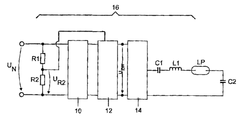
Figure 2 shows a schematic illustration of an exemplary
embodiment of a circuit arrangement according to the invention.
In this case, a system voltage UN, which may be an AC voltage
or a DC voltage, for example from an emergency power supply, is
coupled in a know_z manner to an load circuit via a rectifier
10, an apparatus for system current harmonic correction 12,
which provides the so-called intermediate circuit voltage UZW
at its output, and an inverter 14, the load circuit in this
exemplary embodiment comprising a coupling capacitor C1, an
inductance L1, the electric lamp LP and a resonant capacitor
C2. According to the invention, a voltage divider with
resistors R1 and R2 is provided, the signal tapped of f at the
resistor R2 being fed to the apparatus for system current
harmonic correction 12. The components, starting from the
voltage divider R1, R2 to the inductance Ll, form a drive
circuit 16 for the lamp LP.
A more detailed illustration of the apparatus for system
current harmonic correction 12 can be seen in figure 3. It
shows a step-up converter, which comprises a step-up converter
inductor L2, a switch S1, a diode D1 and a capacitor C3. The
apparatus for system current harmonic correction 12 furthermore
comprises a control unit 18. This control unit 18 is fed the
voltage drop URZ across the resistor R2. The control unit 18
tests whether the voltage URZ has a zero crossing or not. If it
has a zero crossing, it switches to a "transition mode"
operation. If the control unit 18 does not determine a zero
crossing in the voltage URZ, it switches to a "discontinuous
mode" operation. In the transition mode, the switch S1 is
immediately closed again in the event of the current IN through
the step-up converter inductor L2 falling to zero, while, in
the discontinuous mode, there is a wait until a certain
duration Ot has elapsed. This duration Ot is referred to as a
"gap in the current" and is varied according to the invention
CA 02551534 2006-07-04
- 7 - 2005P03137 US-rai
by the control unit 18. The time of a zero value for the
current IN is determined by an additional winding L3 on the
step-up converter inductor L2, whose signal is fed to the
control unit 18 via a resistor R3. The control unit 18 is
moreover fed the value of the voltage UZW across the capacitor
C3 via a line 20, the control unit 18 being designed to
determine the switch-on time ton of the switch S1 such that the
intermediate circuit voltage UZw is as constant as possible.
According to the invention, the duration of the gaps ~t in the
current IN through the step-up converter inductor L2 is varied
between 0.1 ~.s and 20 ~s. In this case, a sweep frequency is
used which is between 0.1 Hz and 100 kHz.
Figure 4 shows the time profile of the current IN through the
step-up converter inductor L2 in the case of a circuit
arrangement according to the invention. It shows that once the
value zero has been first reached, there is a wait for a
duration ~t until the switch S1 of the step-up converter is
closed again, which results in a rising edge of the current IN.
In this case, the gap in the current ~t is approximately 25% of
the period duration. In comparison with figure 1 it can be seen
that the operating frequency has been reduced to 65.7462 kHz,
which corresponds to a frequency reduction of just 40%. In
contrast to this, the peak current has only increased by
approximately 20o to 488 mA.