Note: Descriptions are shown in the official language in which they were submitted.
. ,..."..... ~..a..~,.",..., . -
CA 02551709 2006-07-06
METHODS AND APPARATUS FOR REDUCING A SAMPLING RATE
DURING A SAMPLING PHASE DETERMINATION PROCESS
BACKGROUND
Field of the TechnoloQy
The present invention relates generally to digital communications, and more
particularly to methods and apparatus for reducing a sampling rate during a
sampling
phase determination process.
Description of the Related Art
A wireless communication device, such as a mobile station operating in a
wireless
communication network, may provide for both voice telephony and packet data
communications. The mobile station may, for example, be compatible with 3'~
Generation
(3G) communication standards (e.g. IS-2000) or utilize Global System for
Mobile
Communications (GSM), Time Division Multiple Access (TDMA), or Code Division
Multiple Access (CDMA) wireless technologies.
All such communications utilize radio frequency (RF) signal detection
techniques
in a wireless receiver. Here, RF signals are received through an antenna,
amplified, and
demodulated to recover a digital baseband signal having a symbol or chip
period of T. In
CDMA or direct sequence spread spectrum (DSSS) communications, each symbol is
referred to as a "chip." The baseband signal is sampled by an analog-to-
digital converter
having a sampler which samples the signal at a sampling period which is
determined by a
sampling clock signal. Assuming that a phase of the sampling clock signal can
be finely
adjusted in time so that sampling will occur at the appropriate sampling time
instant, user
or signaling information may be adequately recovered by sampling the baseband
signal at
a sampling period of T (i.e. a sampling frequency or rate of 1/T) which may be
the same as
the symbol or chip period T of the baseband signal.
To find the appropriate phase of the sampling clock signal and thus the
optimal
sampling time point, a sampling phase determination process is performed. The
sampling
phase determination process typically involves oversampling (i.e. sampling at
a sampling
rate greater than 1/T) the baseband signal by n samples per modulation symbol.
The value
of n may be 4 or 8, for example, so that the baseband signal may be
oversampled by as
much as 4 or 8 times (e.g. sample period = Tln = Tl4 or Tl8). Correlation
techniques are
CA 02551709 2006-07-06
then utilized to identify an optimal or maximum correlation result associated
with the
appropriate phase. Subsequently, the baseband signal is down-sampled at the
sampling
period of T at the appropriate phase identified from the sampling phase
determination
process to recover the user or signaling information. This process may be
repeated during
communications to ensure that the sampling clock signal continues to be set at
an
appropriate phase.
In a typical CDMA or DSSS receiver, a searcher is used to determine a signal
delay by correlating samples of the baseband signal with a local pseudorandom
noise (PN)
code. Once the delay of the PN code and the corresponding baseband signal that
produces
the strongest correlation is found, PN code synchronization, bit boundary
synchronization,
the sampling phase determination process are carried out. During the sampling
phase
determination process, each sample set of phase n of the oversampled baseband
signal is
correlated with the local PN. Amongst n correlator outputs, the signal
associated with the
maximum correlation result is associated with the appropriate phase. Usually n
is between
4 and 16, depending on the shaping filter and spreading gain.
A delay locked loop (DLL) may be utilized in lieu of the CDMA searcher to
obtain
a fine determination and tracking of the optimal sample phase, where three
correlators (i.e.
an early correlator, an on-time correlator, and a late correlator) correlates
the PN code with
three sample phases of I-Q signals. Feedback is utilized to adjust the delay
of the samples
until the early and late correlators produce the same output level and the on-
time correlator
produces the highest output level. For TDMA and other non-CDMA communications,
a
timing estimation loop is typically utilized to adjust the sampling time in
accordance with
a criterion that maximizes the "eye-diagram opening." Such schemes also
utilize
oversampling techniques. In lieu of any of the above-described techniques, a
sampling
rate greater than twice the signal bandwidth may be utilized according to the
Shannon
sampling theorem or Nyquist principle, so that optimal sampling points between
available
samples may be interpolated.
In high bandwidth communication systems (e.g. wireless local area network
(WLAN) such as 802.1 lb), high sampling rates require more expensive hardware
(e.g.
analog-to-digital converter, digital processing unit, and/or buffer memory)
and higher
power consumption. For a low-cost, handheld mobile device utilizing one or
more
batteries or a battery pack, these properties are undesirable. Accordingly,
what are needed
2
.. ~ ~. ~,ni~iur.. i~il~~i~I~~.mi n
CA 02551709 2006-07-06
are methods and apparatus for reducing a sampling rate during a sampling phase
determination process so as to overcome the deficiencies in the prior art.
SUMMARY
In one illustrative example of techniques of the present application, a
received
signal is sampled at a sampling period of T + m*(T/n) during a sampling phase
determination process. T may be a symbol or chip period of the received
signal, n is a
number of phases of the sampled signal, T/n is a phase resolution period, and
m is a fixed
non-zero integer value where - n < m < n (e.g. m = 1 or -1 ). By sampling the
received
signal at the sampling period of T + m*(T/n), a sample set for each one of n
phases of the
sampled signal is produced. For each sample set, a correlation process is
performed
between the sample set and a predetermined correlation signal to produce a
correlation
result. Once an optimal correlation result is identified from the correlation
process, the
received signal is sampled at a sampling period of T at a phase associated
with the optimal
correlation result. Advantageously, oversampling at a sampling period of T/n
is not
required during the sampling phase determination process, which reduces cost
and power
consumption.
BRIEF DESCRIPTION OF THE DRAWINGS
Embodiments of present invention will now be described by way of example with
reference to attached figures, wherein:
FIG. 1 is a block diagram which illustrates pertinent components of a mobile
station and a wireless communication network;
FIG. 2 is a more detailed diagram of a preferred mobile station of FIG. 1;
FIG. 3 is a timing diagram which illustrates a plurality of sample points
produced
at a desired sampling period of T which may be equal to a symbol period or
chip period of
a received signal;
FIG. 4 is another timing diagram which illustrates a plurality of sample
points
produced at an oversampling period of T/n during a sampling phase
determination process
of the prior art;
FIG. 5 is a flowchart which describes a method for use in reducing a sampling
rate
during a sampling phase determination process of the present application;
, , . .""", , , ~~ ~, . , . ~, ,
CA 02551709 2006-07-06
FIG. 6 is a timing diagram which illustrates a plurality of sample points
produced
at a sampling period of T + m*(T/n) during the sampling phase determination
process,
where m = -1 and n = 4, which produces a sample set for each one of n phases
of the
sampled signal;
FIG. 7 is another timing diagram which illustrates a plurality of sample
points
produced at a sampling period of T + m*(Tln) during the sampling phase
determination
process, where m = +1 and n = 4, which also produces a sample set for each one
of n
phases of the sampled signal;
FIG. 8 shows a first embodiment of circuitry which may be utilized to
implement
the techniques of the present application;
FIG. 9 is a second embodiment of circuitry which may be utilized to implement
the
techniques of the present application;
FIG. 10 is a schematic block diagram of electronic circuit used for sampling a
received signal according to conventional techniques; and
FIG. 11 is a schematic block diagram of an electronic circuit which may be
utilized
to implement the techniques of the present application.
DETAILED DESCRIPTION OF THE PREFERRED EMBODIMENTS
In one illustrative example of techniques of the present application, a
received
signal is sampled at a sampling period of T + m*(T/n) during a sampling phase
determination process. T may be a symbol or chip period of the received
signal, n is a
number of phases of the sampled signal, T/n is a phase resolution period, and
m is a fixed
non-zero integer value where - n < m < n (e.g. m =1 or -1). By sampling the
received
signal at the sampling period of T + m*(T/n), a sample set for each one of n
phases of the
sampled signal is produced. For each sample set, a correlation process is
performed
between the sample set and a predetermined correlation signal to produce a
correlation
result. Once an optimal correlation result is identified from the correlation
process, the
received signal is sampled at a sampling period of T at a phase associated
with the optimal
correlation result. Advantageously, oversampling at a sampling period of T/n
(where n >
2) is not required during the sampling phase determination process, which may
reduce cost
and power consumption.
4
CA 02551709 2006-07-06
FIG. 1 is a block diagram of a communication system 100, which includes a
mobile station 102, which communicates through a wireless communication
network 104.
Mobile station 102 preferably includes a visual display 112, a keyboard 114,
and perhaps
one or more auxiliary user interfaces (UI) 116, each of which is coupled to a
controller
106. Controller 106 is also coupled to radio frequency (RF) transceiver
circuitry 108 and
an antenna 110. Typically, controller 106 is embodied as a central processing
unit (CPU),
which runs operating system software in a memory component (not shown).
Controller
106 will normally control overall operation of mobile station 102, whereas
signal-
processing operations associated with communication functions are typically
performed in
RF transceiver circuitry 108. Controller 106 interfaces with device display
112 to display
received information, stored information, user inputs, and the like. Keyboard
114, which
may be a telephone type keypad or full alphanumeric keyboard, is normally
provided for
entering data for storage in mobile station 102, information for transmission
to network
104, a telephone number to place a telephone call, commands to be executed on
mobile
station 102, and possibly other or different user inputs.
Mobile station 102 sends communication signals to and receives communication
signals from network 104 over a wireless link via antenna 110. RF transceiver
circuitry
108 performs functions similar to those of a radio network (RN) 128, including
for
example modulation/demodulation and possibly encoding/decoding and
encryptionJdecryption. It is also contemplated that RF transceiver circuitry
108 may
perform certain functions in addition to those performed by RN 128. It will be
apparent to
those skilled in art that RF transceiver circuitry 108 will be adapted to
particular wireless
network or networks in which mobile station 102 is intended to operate.
Mobile station 102 includes a battery interface 122 for receiving one or more
rechargeable batteries 124. Battery 124 provides electrical power to
electrical circuitry in
mobile station 102, and battery interface 122 provides for a mechanical and
electrical
connection for battery 124. Battery interface 122 is coupled to a regulator
126 which
regulates power to the device, providing an output having a regulated voltage
V. Mobile
station 102 also operates using a memory module 120, such as a Subscriber
Identity
Module (SIM) or a Removable User Identity Module (R-UIM), which is connected
to or
inserted in mobile station 102 at an interface 118.
CA 02551709 2006-07-06
Mobile station 102 may consist of a single unit, such as a data communication
device, a cellular telephone, a multiple-function communication device with
data and
voice communication capabilities, a personal digital assistant (PDA) enabled
for wireless
communication, or a computer incorporating an internal modem. Alternatively,
mobile
station 102 may be a multiple-module unit comprising a plurality of separate
components,
including but in no way limited to a computer or other device connected to a
wireless
modem. In particular, for example, in the mobile station block diagram of FIG.
1, RF
transceiver circuitry 108 and antenna 110 may be implemented as a radio modem
unit that
may be inserted into a port on a laptop computer. In this case, the laptop
computer would
include display 112, keyboard 114, one or more auxiliary UIs 116, and
controller 106
embodied as the computer's CPU. It is also contemplated that a computer or
other
equipment not normally capable of wireless communication may be adapted to
connect to
and effectively assume control of RF transceiver circuitry 108 and antenna 110
of a single-
unit device such as one of those described above. Such a mobile station 102
may have a
more particular implementation as described later in relation to mobile
station 202 of FIG.
2.
Mobile station 102 communicates in and through wireless communication network
104. In the embodiment of FIG. l, wireless network 104 is a Third Generation
(3G)
supported network based on Code Division Multiple Access (CDMA) technologies.
In
particular, wireless network 104 is a cdma2000T"'' network which includes
fixed network
components coupled as shown in FIG. 1. Cdma2000~ is a trademark of the
Telecommunications Industry Association (TIA). Wireless network 104 of the
cdma2000-
type includes a Radio Network (RN) 128, a Mobile Switching Center (MSC) 130, a
Signaling System 7 (SS7) network 140, a Home Location Register/Authentication
Center
(HLR/AC) 138, a Packet Data Serving Node (PDSN) 132, an IP network 134, and a
Remote Authentication Dial-In User Service (RADIUS) server 136. SS7 network
140 is
communicatively coupled to a network 142 (such as a Public Switched Telephone
Network or PSTN), whereas IP network is communicatively coupled to a network
144
(such as the Internet).
During operation, mobile station 102 communicates with RN 128, which performs
functions such as call-setup, call processing, and mobility management. RN 128
includes
a plurality of base station transceiver systems that provide wireless network
coverage for a
6
" ~ ",. ,~ " , ,., ~, .~ ,
CA 02551709 2006-07-06
particular coverage area commonly referred to as a "cell". A given base
station
transceiver system of RN 128, such as the one shown in FIG. 1, transmits
communication
signals to and receives communication signals from mobile stations within its
cell. The
base station transceiver system normally performs such functions as modulation
and
possibly encoding andlor encryption of signals to be transmitted to the mobile
station in
accordance with particular, usually predetermined, communication protocols and
parameters, under control of its controller. The base station transceiver
system similarly
demodulates and possibly decodes and decrypts, if necessary, any communication
signals
received from mobile station 102 within its cell. Communication protocols and
parameters may vary between different networks. For example, one network may
employ
a different modulation scheme and operate at different frequencies than other
networks.
The underlying services may also differ based on its particular protocol
revision.
The wireless link shown in communication system 100 of FIG. 1 represents one
or
more different channels, typically different radio frequency (RF) channels,
and associated
protocols used between wireless network 104 and mobile station 102. An RF
channel is a
limited resource that must be conserved, typically due to limits in overall
bandwidth and a
limited battery power of mobile station 102. Those skilled in art will
appreciate that a
wireless network in actual practice may include hundreds of cells depending
upon desired
overall expanse of network coverage. All pertinent components may be connected
by
multiple switches and routers (not shown), controlled by multiple network
controllers.
For all mobile station's 102 registered with a network operator, permanent
data
(such as mobile station 102 user's profile) as well as temporary data (such as
mobile
station's 102 current location) are stored in a HLR/AC 138. In case of a voice
call to
mobile station 102, HLR/AC 138 is queried to determine the current location of
mobile
station 102. A Visitor Location Register (VLR) of MSC 130 is responsible for a
group of
location areas and stores the data of those mobile stations that are currently
in its area of
responsibility. This includes parts of the permanent mobile station data that
have been
transmitted from HLR/AC 138 to the VLR for faster access. However, the VLR of
MSC
130 may also assign and store local data, such as temporary identifications.
HLR/AC 138
also authenticates mobile station 102 on system access.
In order to provide packet data services to mobile station 102 in a cdma2000-
based
network, RN 128 communicates with PDSN 132. PDSN 132 provides access to the
7
,. , ., . " "»,. , . ~~ » ~ ..., ~, . ,
CA 02551709 2006-07-06
Internet 144 (or intranets, Wireless Application Protocol (WAP) servers, etc.)
through IF
network 134. PDSN 132 also provides foreign agent (FA) functionality in mobile
IP
networks as well as packet transport for virtual private networking. PDSN 132
has a range
of IP addresses and performs IP address management, session maintenance, and
optional
caching. RADIUS server 136 is responsible for performing functions related to
authentication, authorization, and accounting (AAA) of packet data services,
and may be
referred to as an AAA server.
Although the system described above relates to cdma2000-based network and
technologies, other suitable networks and technologies may be utilized such as
an 802.11-
based wireless local area network (WLAN).
FIG. 2 is a detailed block diagram of a preferred mobile station 202 utilized
in the
present application. Mobile station 202 is preferably a two-way communication
device
having at least voice and advanced data communication capabilities, including
the
capability to communicate with other computer systems. Depending on the
functionality
provided by mobile station 202, it may be referred to as a data messaging
device, a two-
way pager, a cellular telephone with data messaging capabilities, a wireless
Internet
appliance, or a data communication device (with or without telephony
capabilities).
Mobile station 202 may communicate with any one of a plurality of base station
transceiver systems 200 within its geographic coverage area.
Mobile station 202 will normally incorporate a communication subsystem 211,
which includes a receiver 212, a transmitter 214, and associated components,
such as one
or more (preferably embedded or internal) antenna elements 216 and 218, local
oscillators
(LOs) 213, and a processing module such as a digital signal processor (DSP)
220.
Communication subsystem 211 is analogous to RF transceiver circuitry 108 and
antenna
110 shown in FIG. 1. As will be apparent to those skilled in field of
communications,
particular design of communication subsystem 211 depends on the communication
network in which mobile station 202 is intended to operate.
Mobile station 202 may send and receive communication signals over the network
after required network registration or activation procedures have been
completed. Signals
received by antenna 216 through the network are input to receiver 212, which
may
perform such common receiver functions as signal amplification, frequency down
conversion, filtering, channel selection, and like, and in example shown in
FIG. 2, analog-
i. . 1, "~Yn.iv,i ~..d.eA."Inmr 1
CA 02551709 2006-07-06
to-digital (A/D) conversion. A/D conversion of a received signal allows more
complex
communication functions such as demodulation and decoding to be performed in
DSP
220. In a similar manner, signals to be transmitted are processed, including
modulation
and encoding, for example, by DSP 220. These DSP-processed signals are input
to
transmitter 214 for digital-to-analog (D/A) conversion, frequency up
conversion, filtering,
amplification and transmission over communication network via antenna 218. DSP
220
not only processes communication signals, but also provides for receiver and
transmitter
control. For example, the gains applied to communication signals in receiver
212 and
transmitter 214 may be adaptively controlled through automatic gain control
algorithms
implemented in DSP 220.
Network access is associated with a subscriber or user of mobile station 202,
and
therefore mobile station 202 may require a memory module 262, such as a
Subscriber
Identity Module or "SIM" card or a Removable User Identity Module (R-UIM), to
be
inserted in or connected to an interface 264 of mobile station 202 in order to
operate in the
network. Since mobile station 202 is a mobile battery-powered device, it also
includes a
battery interface 254 for receiving one or more rechargeable batteries 256.
Such a battery
256 provides electrical power to most if not all electrical circuitry in
mobile station 202,
and battery interface 254 provides for a mechanical and electrical connection
for it.
Battery interface 254 is coupled to a regulator (not shown) which regulates
power to all of
the circuitry, providing an output having a regulated voltage V.
Microprocessor 238, which is one implementation of controller 106 of FIG. 1,
controls overall operation of mobile station 202. Communication functions,
including at
least data and voice communications, are performed through communication
subsystem
211. Microprocessor 238 also interacts with additional device subsystems such
as a
display 222, a flash memory 224, a random access memory (RAM) 226, auxiliary
inputloutput (I/O) subsystems 228, a serial port 230, a keyboard 232, a
speaker 234, a
microphone 236, a short-range communications subsystem 240, and any other
device
subsystems generally designated at 242. Some of the subsystems shown in FIG. 2
perform
communication-related functions, whereas other subsystems may provide
"resident" or on-
device functions. Notably, some subsystems, such as keyboard 232 and display
222, for
example, may be used for both communication-related functions, such as
entering a text
message for transmission over a communication network, and device-resident
functions
9
CA 02551709 2006-07-06
such as a calculator or task list. Operating system software used by
microprocessor 238 is
preferably stored in a persistent store such as flash memory 224, which may
alternatively
be a read-only memory (ROM) or similar storage element (not shown). Those
skilled in
the art will appreciate that the operating system, specific device
applications, or parts
thereof, may be temporarily loaded into a volatile store such as RAM 226.
Microprocessor 238, in addition to its operating system functions, preferably
enables execution of software applications on mobile station 202. A
predetermined set of
applications, which control basic device operations, including at least data
and voice
communication applications, will normally be installed on mobile station 202
during its
manufacture. A preferred application that may be loaded onto mobile station
202 may be
a personal information manager (PIM) application having the ability to
organize and
manage data items relating to user such as, but not limited to, e-mail,
calendar events,
voice mails, appointments, and task items. Naturally, one or more memory
stores are
available on mobile station 202 and SIM 256 to facilitate storage of PIM data
items and
other information.
The PIM application preferably has the ability to send and receive data items
via
the wireless network. In a preferred embodiment, PIM data items are seamlessly
integrated, synchronized, and updated via the wireless network, with the
mobile station
user's corresponding data items stored and/or associated with a host computer
system
thereby creating a mirrored host computer on mobile station 202 with respect
to such
items. This is especially advantageous where the host computer system is the
mobile
station user's office computer system. Additional applications may also be
loaded onto
mobile station 202 through network, an auxiliary I/O subsystem 228, serial
port 230,
short-range communications subsystem 240, or any other suitable subsystem 242,
and
installed by a user in RAM 226 or preferably a non-volatile store (not shown)
for
execution by microprocessor 238. Such flexibility in application installation
increases the
functionality of mobile station 202 and may provide enhanced on-device
functions,
communication-related functions, or both. For example, secure communication
applications may enable electronic commerce functions and other such financial
transactions to be performed using mobile station 202.
In a data communication mode, a received signal such as a text message, an e-
mail
message, or web page download will be processed by communication subsystem 211
and
.. r. 1 . ~ .".rr.r, i -. vl .w n n 1 w n. i .
CA 02551709 2006-07-06
input to microprocessor 238. Microprocessor 238 will preferably further
process the
signal for output to display 222 or alternatively to auxiliary I/O device 228.
A user of
mobile station 202 may also compose data items, such as e-mail messages, for
example,
using keyboard 232 in conjunction with display 222 and possibly auxiliary I/O
device 228.
Keyboard 232 is preferably a complete alphanumeric keyboard and/or telephone-
type
keypad. These composed items may be transmitted over a communication network
through communication subsystem 211.
For voice communications, the overall operation of mobile station 202 is
substantially similar, except that the received signals would be output to
speaker 234 and
signals for transmission would be generated by microphone 236. Alternative
voice or
audio I/O subsystems, such as a voice message recording subsystem, may also be
implemented on mobile station 202. Although voice or audio signal output is
preferably
accomplished primarily through speaker 234, display 222 may also be used to
provide an
indication of the identity of a calling party, duration of a voice call, or
other voice call
related information, as some examples.
Serial port 230 in FIG. 2 is normally implemented in a personal digital
assistant
(PDA)-type communication device for which synchronization with a user's
desktop
computer is a desirable, albeit optional, component. Serial port 230 enables a
user to set
preferences through an external device or software application and extends the
capabilities
of mobile station 202 by providing for information or software downloads to
mobile
station 202 other than through a wireless communication network. The alternate
download path may, for example, be used to load an encryption key onto mobile
station
202 through a direct and thus reliable and trusted connection to thereby
provide secure
device communication.
Short-range communications subsystem 240 of FIG. 2 is an additional optional
component, which provides for communication between mobile station 202 and
different
systems or devices, which need not necessarily be similar devices. For
example,
subsystem 240 may include an infrared device and associated circuits and
components, or
a Bluetooth'~ communication module to provide for communication with similarly
enabled systems and devices. Bluetooth~ is a registered trademark of Bluetooth
SIG,
Inc.
11
.. , , . ,..",»,. , ."...,...,., .., , ,
CA 02551709 2006-07-06
During communications, RF signals are received through antenna 216, amplified
and demodulated in receiver 212, so that a digital baseband signal having a
symbol period
of T may be recovered. The digital baseband signal is sampled by an analog-to-
digital
converter of receiver 212 which includes a sampler which samples the signal at
a sampling
period which is determined by a sampling clock signal. Assuming that a phase
of the
sampling clock signal can be finely adjusted in time so that sampling will
occur at the
appropriate sampling time instant, user or signaling information may be
adequately
recovered by sampling the baseband signal at a sampling period of T (i.e. a
sampling
frequency or rate of 1lT) which may be the same as the symbol or chip period
of the
baseband signal.
FIG. 3 is a timing diagram which illustrates a plurality of sample points 302
(such
as a sample point 304) produced with use of a first sampling clock signal
having the
sampling period of T. The sampling signal having the sampling period of T is
utilized to
sample the baseband signal during a normal communication mode when the
baseband
signal comprises user or signaling information. The sampling period of T may
be equal to
a symbol or chip period T of the received baseband signal which is currently
being
sampled. It is indeed viable to sample the baseband signal having the symbol
or chip
period of T with a sampling signal having the period of T and adequately
recover the user
or signaling information from the baseband signal as long as the samples are
taken at an
optimal instant in time (i.e. assuming that the phase of the sampling clock
signal can be
finely adjusted in time so that sampling will occur at the appropriate
sampling time
instant).
In FIG. 4, another timing diagram which illustrates a plurality of sample
points 402
(such as a sample point 404) produced with use of a second sampling clock
signal having
a sampling period of T/n (i.e. an oversampling rate of n/T). The second
sampling clock
signal having the sampling period of T/n may be utilized to sample the
baseband signal
during a sampling phase determination process of the prior art. The baseband
signal
which is sampled in the sampling phase determination process comprises a
predetermined
code which may be synchronization information or preamble information. In the
sampling
phase determination mode, correlation techniques are utilized to identify an
optimal or
maximum correlation result associated with a desired phase of the sampling
clock signal.
Subsequently, the baseband signal is sampled with use of the first sampling
clock signal
12
. . n. .....u... ~-.d..v-..Lm...i 1..
CA 02551709 2006-07-06
having the sampling period of T at this desired phase in order to adequately
recover the
user or signaling information from the baseband signal (see FIG. 3).
Note that the value of n for oversampling may be any suitable value such as a
fixed
value between 4 and 16. Therefore, the oversampling period of the prior art is
a fixed
value which may be between about T/4 to T/16. In high bandwidth communication
systems, high sampling rates require more expensive hardware (e.g. analog-to-
digital
converter, digital processing unit, and/or buffer memory) and higher power
consumption.
For Universal Mobile Telephony System (UMTS), the chip rate is 3.84 MHz which
corresponds to a sampling rate of 30.72 MHz if the over sampling factor n is
equal to 8.
For an 802.11-based wireless local area network (WLAI~, the chip rate is 11
MHz which
corresponds to a sampling rate of 88 MHz if the over sampling factor n is
equal to 8.
Especially for a low-cost, handheld mobile device utilizing one or more
batteries or a
battery pack, it is not desirable to have relatively expensive hardware and
high power
consumption.
FIG. 5 is a flowchart which describes a general method for use in reducing a
sampling rate during a sampling phase determination process for the mobile
station of
FIGs. 1 and 2. Beginning at a start block 502 of FIG. 5, a received baseband
signal is
sampled at a fixed sampling period of T' = T + m*(T/n) during a sampling phase
determination process (step 504 of FIG. 5). The value T is a sampling period
utilized for
sampling the received signal after the sampling phase determination process is
completed.
Preferably, T is also the symbol period or chip period of the received signal.
The value n
is the number of phases of the sampled signal and T/n is a phase resolution
period. The
value of n may be four (4) or eight (8), for example, or any other suitable
value (e.g.
between 2 and 20).
The value m is a non-zero integer value where - n < m < n. Preferably, the
sampling period of T' = T + m*(T/n) is set just slightly higher or lower than
the sampling
period T by selecting a suitable value of m. For example, the sampling period
of T' = T +
m*(T/n) may be set just slightly higher or lower than the sampling period T by
a single
sampling phase where m = 1 or -1. Illustrative examples of sampling periods of
T' = T +
m*(T/n) are shown and described later below in relation to FIGS. 6 and 7. Note
that,
during the sampling phase determination process of step 504 of FIG. 5, a high
oversampling rate of n/T is not utilized.
13
M ""~",
CA 02551709 2006-07-06
The baseband signal which is sampled in the sampling phase determination
process
may comprise a predetermined code, which may be synchronization information or
preamble information. By sampling the received signal at a sampling period of
T' = T +
m*(T/n), a sample set for each one of n phases of the sampled signal is
produced. For
each sample set, a correlation process between the sample set at phase i
(where i = 0, 1,
. . ., n) and a predetermined correlation signal at the corresponding time of
the samples of
the sample set is performed so that a correlation result is produced (step 506
of FIG. 5).
Illustrative examples of sample sets are shown and described later below in
relation to
FIGS. 6 and 7. In the CDMA environment, the predetermined correlation signal
is a
predetermined pseudorandom noise (PN) signal. From step 506, a plurality of n
correlation results associated with the plurality of n sample sets are
produced. An
optimum or maximum correlation result is then identified from all of the
correlation
results; this optimum or maximum correlation result is associated with one of
the n phases.
The received signal is then sampled at a sampling period of T at the phase
associated with
an optimal correlation result (step 508 of FIG. 5). At this time, the received
signal
comprises user or signaling information during a normal communication mode
which is
recovered. The flowchart ends at a finish block 508, but may repeat each time
the
sampling phase may need to be updated.
FIG. 6 is a timing diagram which illustrates an example of a plurality of
sample
points 602 (such as a sampling point 604) produced at a sampling period of T'
= T +
m*(T/n) during the sampling phase determination process in step 504 of FIG. S.
In this
example, n = 4 and m = -1 so that the sampling period during the sampling
phase
determination process is T' = T(n - 1 )/n = 3T14. As apparent, the sampling
period is set
just slightly shorter than the sampling period T by a single sampling phase.
As shown in
FIG. 6, a sample set for each one of n phases (phases 0 through 3) of the
sampled signal is
produced. The sample sets include a first sample set 606 at phase 0 which is
associated
with sample points at time 0, time 3T, time 6T, time 9T, etc.; a second sample
set 608 at
phase 1 which is associated with sample points at time 0 + 3T/4, time 3T +
3T/4, time 6T
+ 3T/4, time 9T + 3T/4, etc.; a third sample set 610 at phase 2 which is
associated with
sample points at time T + 2T/4, time 4T + 2T/4, time 7T + 2T/4, time l OT +
2T/4, etc.;
and a fourth sample set 612 at phase 3 which is associated with sample points
at time 2T +
14
CA 02551709 2006-07-06
T/4, ST + T/4, 8T + T14, 11T + T14, etc. Each one of these sample sets is
utilized in a
correlation process in step 506 of FIG. 5.
FIG. 7 is a timing diagram which illustrates another example of a plurality of
sample points (such as a sampling point 704) produced at a sampling period of
T' = T +
m*(T/n) during the sampling phase determination process in step 504 of FIG. 5.
In this
example, n = 4 and m = +1 so that the sampling period during the sampling
phase
determination process is T' = T(n + 1 )/n = ST/4. As apparent, this sampling
period is set
just slightly longer than the sampling period T by a single sampling phase. As
shown in
FIG. 7, a sample set for each one of n phases (phases 0 through 3) of the
sampled signal is
produced. The sample sets include a first sample set 706 at phase 0 which is
associated
with sample points at time 0, time ST, time IOT, etc.; a second sample set 708
at phase 1
which is associated with sample points at time T + T/4, time 6T + T/4, time 11
T + T/4;
etc,; a third sample set 710 at phase 2 which is associated with sample points
at time 2T +
2T/4, time 7T + 2T/4, time 12T + 2T/4, etc.; and a fourth sample set 712 at
phase 3 which
is associated with sample points at time 3T + 3T/4, 8T + 3T/4, etc. Each one
of these
sample sets is utilized in a correlation process in step 506 of FIG. 5.
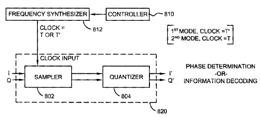
FIG. 8 shows a first embodiment of circuitry which may be utilized to
implement
the techniques of the present application, as described in relation to FIGs. 5-
7 above. The
circuitry of FIG. 8 includes control circuitry or controller 810 (e.g.
controller 106 of FIG.
1 or microprocessor 238 of FIG. 2), a frequency synthesizer 812 with phase
control, and
an analog-to-digital converter 820. Analog-to-digital converter 820 includes a
sampler
802 and a quantizer 804. I and Q analog baseband signals are received at
inputs to
sampler 802, which samples the signals to produce sampled I and Q baseband
signals at its
outputs. The sampled I and Q baseband signals are fed into inputs to quantizer
804, which
quantizes the signals to produce digital I' and Q' baseband signals at its
outputs. Sampler
802 has a clock input which is coupled to a clock output from frequency
synthesizer 812.
Frequency synthesizer 812 is adapted to produce, at its clock output, a
sampling clock
signal having one of a plurality of different frequencies as controlled by
controller 810.
Since frequency synthesizer 812 has phase control, it has additional
functionality to select
a phase of the sampling clock signal as well.
Frequency synthesizer 812 is set or programmed by controller 810 to produce
the
sampling clock signal at its clock output. Specifically, controller 810 of
FIG. 8 is adapted
... w L. ~ i,~"r.rrrm. ~ ~ rl rr r..r.3v m, n p ~~
CA 02551709 2006-07-06
or programmed to set frequency synthesizer 812 to pmduce a sampling clock
signal
having a period of T' = T + m*(TJn) during a sampling phase determination mode
(e.g. for
step 504 of FIG. 5 and FIG. 6 or 7). During the sampling phase determination
mode, the
received signal may comprise a predetermined code. During a normal
communication
mode (e.g. for step 508 of FIG. 5), controller 810 is adapted or programmed to
set
frequency synthesizer 812 to produce a sampling clock signal having a period
of T and a
phase that is determined from the sampling phase determination mode. During
the normal
communication mode, the received signal comprises user or signaling
information.
With use of the circuit of FIG. 8, the sampling phase determination mode
occurs
during a first time period and the normal communication mode occurs during a
second
time period which follows the first dme period. The sampling phase
determination mode
may be performed again each time the predetermined code is transmitted and/or
when the
sampling phase may need updating.
FIG. 9 is a second embodiment of circuitry which may be utilized to implement
the
techniques of the present application, as described in relation to FIGS. 5-8.
The circuitry
of FIG. 9 includes control circuitry or controller 810 (e.g. controller 106 of
FIG. 1 or
microprocessor 238 of FIG. 2), frequency synthesizer 812 having phase control,
two
analog-to-digital converters 820 and 920, an optimal phase determination block
908, and
an informationJsignaling decoding block or decoder 910. Analog-to-digital
converter 820
was described above in relation to FIG. 8 and operates in substantially the
same way,
except that it operates only on a received signal comprising the user or
signaling
information. I' and Q' outputs from quantizer 804 are coupled to
informationJsignaling
decoding block 910 to process information or signaling in a conventional
fashion (e.g.
despreading and decoding the information).
On the other hand, analog-to-digital converter 920 operates exclusively for
the
sampling phase determination process. Analog-to-digital converter 920 is
similar to
analog-to-digital converter 820 and includes a sampler 902 and a quantizer
904. The I and
Q analog baseband signals are received at inputs to sampler 902, which samples
the
signals to produce sampled I and Q baseband signals at its outputs. Sampler
902 has a
clock input which is coupled to a clock output from frequency synthesizer 812.
The
sampled I and Q baseband signals are fed into inputs to quantizer 904, which
quantizes the
signals to produce digital I" and Q" baseband signals at its outputs. The r'
and Q" outputs
16
CA 02551709 2006-07-06
from quantizer 904 are coupled to inputs to phase determination block 908,
which operates
to identify the optimal phase result of the signal. An output from phase
determination
block 908 is coupled to an input to controller 810 for providing the optimal
phase result to
controller 810.
Frequency synthesizer 812 is set or programmed by controller 810 to produce
sampling clock signals for both sampler 802 and sampler 902. In particular,
controller 810
of FIG. 9 is adapted or programmed to set frequency synthesizer 812 to produce
a first
sampling clock signal having a period of T' = T + m*(T/n) for sampler 902
(e.g. for step
504 of FIG. 5, and FIG. 6 or 7). This is done for the sampling phase
determination
process. Phase determination block 908 identifies the optimal phase result
from the I" and
Q" signals from quantizer 904 and provides this result to controller 810.
Controller 810 is
also adapted or programmed to set frequency synthesizer 812 to produce a
second
sampling clock signal having a period of T for sampler 802 (e.g. for step 508
of FIG. 5).
Here, controller 810 uses the optimal phase result from phase determination
block 908 to
set the appropriate optimal phase of the second sampling clock signal. This is
done for
information/signaling decoding.
Thus, with use of the circuit of FIG. 9, the sampling phase determination mode
is
performed with use of a first analog-to-digital converter and the normal
communication
mode is performed with use of a second analog-to-digital converter. The first
and second
clock signals may be simultaneously generated, or analog-to-digital converters
802 and
902 may operate over the same time periods.
FIG. 10 is a schematic block diagram of a conventional electronic circuit 1000
used as part of a correlator searcher. The electronic circuit 1000 includes an
analog-to-
digital converter 1020, a plurality of n downsamplers 1004, a plurality of n
correlators
1014, a pseudorandom noise (PN) code generator 1012, an optimal level detector
1022,
and a selector 1024 (e.g, a multiplexer). I and Q baseband signals are
received at inputs to
analog-to-digital converter 1020. Outputs from analog-to-digital converter
1020 are
coupled to and provide digitized I and Q baseband signals to each input of
downsamplers
1004. Outputs from each downsampler 1004 are coupled to and provide only a
selected
phase of the digitized I and Q baseband signals to a corresponding correlator
1014. The
outputs from each downsampler 1004 are also coupled to inputs to selector
1024. An
output from PN generator 1012 is coupled to and produces a PN code at each
input of
17
CA 02551709 2006-07-06
correlators 1014, which have outputs coupled to optimal level detector 1022.
An output
from optimal level detector 1022 is coupled to an input to selector 1024 for
providing a
selection signal to selector 1024. The selection signal is used at selector
1024 for selecting
and providing one set of inputs from a downsamplers 1004 to an output from
selector 1024
for additional processing.
A sampling phase determination process using electronic circuit 1000 typically
involves oversampling the baseband signal by n samples per modulation symbol
or chip
using analog-to-digital converter 1020. The value of n may be 4 or 8, for
example, so that
the baseband signal may be oversampled by as much as 4 or 8 times (e.g. sample
period =
T/n = T/4 or T/8). Using downsampler 1004, PN code generator 1012, and
correlators
1014, a correlation process between each baseband signal at one of the n
phases
respectively and a PN code is performed. An optimal or maximum correlation
result
associated with the appropriate phase is identified with use of optimal level
detector 1022.
Subsequently, the baseband signal is sampled at the sampling period of T with
analog-to-
digital converter 1020 at the appropriate phase identified from the sampling
phase
determination process to recover the user or signaling information.
Alternatively, selector
1024 is not needed where sampling at both T/n and T is continuously and
simultaneously
performed on the received signal.
FIG. 11 is a schematic block diagram of an electronic circuit 1100 used as
part of a
correlator searcher in accordance with techniques of the present application,
as described
above in relation to FIGs. S-8. The electronic circuit 1100 includes analog-to-
digital
converter 820 (e.g. see FIG. 8), a plurality of n downsamplers 1104 for the
received
baseband signal (one for each phase 0 through n-1), a plurality of n
downsamplers 1106
for a predetermined code signal (one for each phase 0 through n-1), a
predetermined code
generator 1112 (e.g. a PN code generator), a plurality of n correlators 1114,
an optimal
level detector 1122, and a clock frequency and phase controller 1124. I and Q
baseband
signals are received at inputs to analog-to-digital converter 820. Outputs
from analog-to-
digital converter 820 are coupled and provide digitized I and Q baseband
signals to each
input of downsamplers 1104. Outputs from each downsamplers 1104 are coupled to
and
provide only a selected phase of the digitized I and Q baseband signals to a
corresponding
correlator 1114. An output from predetermined code generator 1112 is coupled
to and
produces a predetermined correlation signal at each input of con elators 1114,
which have
18
CA 02551709 2006-07-06
outputs coupled to optimal level detector 1122. An output from optimal level
detector has
an output coupled to an input to clock frequency and phase controller 1124 for
providing a
selection signal.
A sampling phase determination process using electronic circuit 1100 involves
sampling the baseband signal at a sampling period of T' = T + m*(T/n) using
analog-to-
digital converter 820 which is under control by clock frequency and phase
controller 1124,
as described above in relation to FIGs. S-9. Here, a sample set for each one
of n phases of
the sampled signal is received at a corresponding one of the downsamplers
1104. Using
downsamplers 1104 and 1106, predetermined code generator 1112, and correlators
1114, a
correlation process between each baseband signal at one of the n phases and a
predetermined code at the corresponding phase is performed. The down sampling
factor
for each downsampler 1104 is n, whereas the down sampling factor for each
downsampler
1106 is n' = n + m. An optimal or maximum correlation result associated with
the
appropriate phase is then identified with use of optimal level detector 1122.
Subsequently,
the baseband signal is sampled at the sampling period of T with analog-to-
digital converter
820 at the appropriate phase identified from the sampling phase determination
process to
recover the user or signaling information.
A delay locked loop (DLL) may be utilized in lieu of the CDMA searcher for
fine
delay determination, where three correlators (i.e. an early correlator, an on-
time correlator,
and a late correlator) correlate the PN code with samples of three I-Q
signals. A CDMA
search may still be needed for a coarse delay determination. In general,
feedback is
utilized to adjust the delay of the samples until the early and late
correlators produce the
same output level and the on-time correlator produces the highest output
level.
Suppose the transmission mode of a given CDMA system is continuous and may
last for a relatively long time. Alternatively, suppose that although
transmission is in burst
mode, between bursts the time and frequency relation are synchronized to the
same stable
source at the transmitter and the propagation path delays are relatively slow-
varying
relative to the time span between bursts. Given these conditions, a DLL-based
solution to
track optimal timing is preferred. In such system, the DLL typically needs to
be initialized
to a predetermined approximate optimal sampling time but subsequently it
handles
tracking the changes in the optimal sampling instant. The task to select and
assign an
initial approximate optimal sampling point to the DLL is accomplished by the
searcher-
19
n r . .F . ~..,r.e... n r il ...n.~ ." n. i r ~.
CA 02551709 2006-07-06
based solution described earlier. Subsequent to the initial selection, an
alternative
technique is utilized which is now described.
For the DLL technique, electronic circuit 1100 of FIG. 11 may be utilized
where
three (3) downsamplers 1104 are utilized for early, mid, and late phases and
three (3)
downsamplers 1106 are utilized for the same three phases. Optimal level
detector 1122 of
FIG. 11 is instead a delay adjustor 1122.
Suppose there are either pilot symbols embedded in the data stream
periodically or
there are preambles in at least some bursts in a regular or periodic fashion.
The pilot
symbols or the preambles do not overlap with the intended information stream
in time and
may be used for DLL tracking purpose. During the pilot symbol or preamble, the
receiver
is in a DLL mode and DLL components are enabled. Outside the pilot symbol or
preamble periods, the receiver is in a normal communication mode where the DLL
components are disabled; however the previous timing phase result is stored
and used
again when the DLL mode is re-enabled.
In the DLL mode, clock frequency and phase controller 1124 generates a
sampling
clock signal having a sampling period of T' and the sampled I-Q stream are
downsampled
by a factor n at 3 different phases: the early phase, the mid (or on-time)
phase, and the late
phase. A PN code is generated by predetermined code generator 1112 and
downsampled
by n' = n + m. The downsampled I-Q and downsampled PN are correlated by the
early,
mid, and late correlators 1114. Delay adjustor 1122 makes the decision of
delay
adjustment based on the three correlator output values. This is the same as in
a
conventional DLL. An output from delay adjustor 1122 controls the phase of the
early,
mid, and late downsamplers to move forward or backward by the same amount.
When the
effective sampling point moves across a PN symbol boundary, the downsampler
for the
PN also needs to adjust and the above process is repeated. This way, the mid
(on-time)
phase always tracks the optimal sampling point. In the normal communication
mode,
clock frequency and phase controller 1124 generates the sampling signal at a
sampling
period of T at the updated optimal phase that the DLL mode identified for the
mid (on-
time) phase. The sampled I-Q and the PN are ready to be passed to further
processing.
In other embodiments, for TDMA and other non-CDMA communications, for
example, a timing estimation loop is typically utilized to adjust the sampling
time in
accordance with a criterion that maximizes the "eye-diagram opening." The
techniques of
r. s..4.wr,vrnm~r r.rlrr a..,in-.,.rv...~.,
CA 02551709 2006-07-06
the present application may be utilized in these TDMA and other non-CDMA
communication in the same or similar fashion.
Final Comments. Methods and apparatus for use in reducing a sampling rate
during a sampling phase determination process have been described. In one
illustrative
example, a received signal is sampled at a sampling period of T + m*(T/n)
during a
sampling phase determination process. T may be a symbol or chip period of the
received
signal, n is a number of phases of the sampled signal, T/n is a phase
resolution period, and
m is a fixed non-zero integer value where - n < m < n (e.g. m =1 or -1 ). By
sampling the
received signal at the sampling period of T + m*(T/n), a sample set for each
one of n
phases of the sampled signal is produced. For each sample set, a correlation
process is
performed between the sample set and a predetermined correlation signal to
produce a
correlation result. Once an optimal correlation result is identified from the
correlation
process, the received signal is sampled at a sampling period of T at a phase
associated with
the optimal correlation result. Advantageously, oversampling at a sampling
period of T/n
is not required during the sampling phase determination process, which reduces
cost and
power consumption.
An electronic circuit of the present application comprises control circuitry,
an
analog-to-digital converter which includes a sampler, and a plurality of n
correlators. The
control circuitry is adapted to cause the sampler to sample a received signal
at a sampling
period of T + m*(T/n) during a sampling phase determination process, where n
is the
number of phases of the sampled signal, T/n is a phase resolution period, and
m is a non-
zero integer value where - n < m < n (e.g. m = 1 or -1). During the sampling
phase
determination process, an output from the sampler provides a sample set for
each one of n
phases of the sampled signal. Each correlator of the plurality of n
correlators has a first
input adapted to receive one of the sample sets associated with a
corresponding one of the
n phases of the sampled signal, a second input adapted to receive a
predetermined
correlation signal, and an output which provides a correlation result from a
correlation
process between the sample set and the predetermined correlation signal. The
control
circuitry is further adapted to cause the sampler to sample the received
signal at a
sampling period of T at one of the n phases associated with an optimal
correlation result.
A communication device of the present application includes a wireless
receiver, a
frequency synthesizer of the wireless receiver, control circuitry coupled to
the frequency
21
r ..A , ~.a..n~.., .,I .w,...ie .. ,...k "
CA 02551709 2006-07-06
synthesizer; and an analog-to-digital converter. The analog-to-digital
converter has a
sampler, an input for receiving a signal through the wireless receiver, a
clock input
coupled to a clock output of the frequency synthesizer, and an output. The
control
circuitry is adapted to set the frequency synthesizer to produce a clock
signal at the clock
output so that the sampler samples the received signal at a sampling period of
T + m*(T/n)
during a sampling phase determination process, where n is the number of phases
of the
sampled signal, T/n is a phase resolution period, and m is a non-zero integer
value where -
n < m < n (e.g. m =1 or -1). During the sampling phase determination process,
the output
from the analog-to-digital converter provides a sample set for each one of n
phases of the
sampled signal. Each correlator of the plurality of n correlators has a first
input adapted to
receive one of the sample sets associated with a corresponding one of the n
phases of the
sampled signal, a second input adapted to receive a predetermined correlation
signal, and
an output which provides a correlation result from a correlation process
between the
sample set and the predetermined correlation signal. The control circuitry is
further
adapted to set the frequency synthesizer to produce a clock signal at the
clock output so
that the sampler samples the received signal at a sampling period of T at one
of the n
phases associated with an optimal correlation result, in an operation mode
other than the
sampling phase determination process.
The above-described embodiments of the present application are intended to be
examples only. Those of skill in the art may effect alterations, modifications
and
variations to the particular embodiments without departing from the scope of
the
application. The invention described herein in the recited claims intends to
cover and
embrace all suitable changes in technology.
22