Language selection

Search

Patent 2552089 Summary

Third-party information liability

Some of the information on this Web page has been provided by external sources. The Government of Canada is not responsible for the accuracy, reliability or currency of the information supplied by external sources. Users wishing to rely upon this information should consult directly with the source of the information. Content provided by external sources is not subject to official languages, privacy and accessibility requirements.

Claims and Abstract availability

Any discrepancies in the text and image of the Claims and Abstract are due to differing posting times. Text of the Claims and Abstract are posted:

  • At the time the application is open to public inspection;
  • At the time of issue of the patent (grant).
(12) Patent: (11) CA 2552089
(54) English Title: CIRCUIT BOARD MOUNTING BRACKET
(54) French Title: SUPPORT DE MONTAGE D'UNE CARTE DE CIRCUITS IMPRIMES
Status: Granted
Bibliographic Data
(51) International Patent Classification (IPC):
  • H01R 4/66 (2006.01)
(72) Inventors :
  • BRUNO, DAVID J. (United States of America)
(73) Owners :
  • PEM MANAGEMENT, INC. (United States of America)
(71) Applicants :
  • PEM MANAGEMENT, INC. (United States of America)
(74) Agent: SMART & BIGGAR LP
(74) Associate agent:
(45) Issued: 2010-07-27
(86) PCT Filing Date: 2005-02-11
(87) Open to Public Inspection: 2005-09-01
Examination requested: 2007-08-23
Availability of licence: N/A
(25) Language of filing: English

Patent Cooperation Treaty (PCT): Yes
(86) PCT Filing Number: PCT/US2005/004016
(87) International Publication Number: WO2005/079249
(85) National Entry: 2006-06-28

(30) Application Priority Data:
Application No. Country/Territory Date
60/544,309 United States of America 2004-02-17

Abstracts

English Abstract


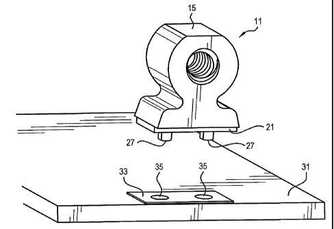
A pick-and-place type circuit board mounting bracket is surface-mounted, or
alternatively, soldered with reinforcing posts that occupy one or more
through~holes in the circuit board. The mounting face of the bracket is offset
with respect to its mounting base to allow the face of the bracket to be sub-
flush, flush, or extend beyond the edge of the circuit board. The front
surface of the bracket is preferably perpendicular to the bottom surface and a
longitudinal threaded bore extends through the main body to provide attachment
means for affixing structures to the bracket. The posts which extend
downwardly through the circuit board may have at least one planar side surface
or a single rectangular post may be employed. The length of the posts is
preferably less than the thickness of the circuit board for surface mount
applications or long enough to extend through the circuit board for wave
soldering.


French Abstract

L'invention concerne un support de montage de carte de circuits imprimés de type transfert, qui est monté sur une surface, ou en variante, soudé au moyen de montants de renforcement occupant au moins un trou traversant de la carte de circuits imprimés. La face de montage du support est décalée par rapport à la base de montage pour permettre à la face du support d'être en renfoncement, alignée avec la base, de s'étendre au-delà du bord de la carte de circuits imprimés. La surface avant du support est de préférence perpendiculaire à la surface de fond, et un alésage fileté longitudinal s'étend à travers le corps principal pour fournir un moyen de fixation permettant de fixer des structures au support. Les montants qui s'étendent vers le bas, en traversant la carte de circuits imprimés, peuvent présenter au moins une surface latérale plane, ou un montant rectangulaire unique peut être utilisé. La longueur des montants est de préférence inférieure à l'épaisseur de la carte de circuits imprimés pour des applications de montage de surface ou assez longue pour s'étendre à travers la carte de circuits imprimés pour une soudure à vague.

Claims

Note: Claims are shown in the official language in which they were submitted.


CLAIMS

What is claimed is:

1. ~A bracket for attachment to a circuit board, comprising:
a main body having a planar front surface including a bottom edge;
attachment means on said main body for affixation to said front
surface;~
a centered planar top surface of said main body adapted for pick-
and-place transportation of the bracket; and
a base beneath the bottom edge of said front surface, said base
having a front side parallel to said front surface and offset rearwardly
therefrom,
said base further including a planar bottom surface adapted for mounting to a
circuit board.

2. ~The bracket of claim 1 wherein said base further includes at least
one post extending downwardly from said bottom surface.

3. ~The bracket of claim 2 further including a longitudinal threaded
bore extending through said front surface.

4. ~The bracket of claim 2 which includes only two posts.

5. ~An assembly of parts including the bracket of claim 2 and a circuit
board having an aperture receiving each post of said bracket.

6. ~The circuit board and bracket assembly of claim 5 wherein the front
surface is co-planar with a side edge of said circuit board.

7. ~The circuit board and bracket assembly of claim 5 further including
a solder joint between said base and circuit board which rigidly affixes said
bracket
to said circuit board.
7


8. ~The circuit board and bracket assembly of claim 7 wherein the
length of said posts is less than the thickness of the circuit board.

9. ~The bracket of claim 2 wherein said posts are unitary with the main
body.

10. ~The bracket of claim 1 wherein the front surface is perpendicular to
the bottom surface.

11. ~The bracket of claim 1 further including a single post with at least
one planar side surface, said post extending downwardly from said bottom
surface.

12. ~An assembly of parts including the bracket of claim 1 and a circuit
board including a solder joint between said bottom surface of the base and the
circuit board.

13. ~The circuit board and bracket assembly of claim 5 wherein the front
surface extends beyond a side edge of the circuit board and wherein the bottom
surface does not cover a portion of a top surface of the circuit board in
front of the
base.

8

Description

Note: Descriptions are shown in the official language in which they were submitted.


CA 02552089 2006-06-28
WO 2005/079249 PCT/US2005/004016
1 CIRCUIT BOARD MOUNTING BRACKET
2
3 RELATED APPLICATIONS
4 The present application is related to provisional patent application serial
number 60/544,309 entitled "Circuit Board Mounting Bracket" filed on February
6 17, 2004, priority from which is hereby claimed.
7 FIELD OF THE INVENTION
8 The present invention relates to fasteners and types of hardware for circuit
9 boards. More specifically, it relates to a right-angle mounting bracket for
a circuit
board which can be surface-mounted by soldering.
11 BACKGROUND OF THE INVENTION AND PRIOR ART
12 There are many mounting brackets that provide mounting attachment at a
13 right angle from a surface. A particular bracket is disclosed, for example,
in U. S.
14 Patent 5,810,501 entitled "Perpendicular Edge Fastener." The device in this
patent
includes a rectangular base which provides clinch-type attachment of the
bracket to
16 a metal sheet. There is, however, a great demand for mounting brackets for
circuit
17 boards, but this device is not suitable for circuit board applications.
Heretofore
18 none has been devised which may be most ei~ciently used as a versatile
right-angle
19 circuit board surface mount bracket. One requirement for a circuit board
bracket is
its ability to provide a vertical attachment face which is flush with or
extends
21 beyond the edge of the circuit board, however this desired mounting
position poses
22 several problems. First, to be eiI'iciently used in high volume circuit
board
23 production, the mounting bracket is often required to be transported to the
circuit
24 board by automated pick-and-place equipment. Such equipment requires a
1


CA 02552089 2006-06-28
WO 2005/079249 PCT/US2005/004016
1 centered, flat top surface so that the device can be handled by the vacuum
2 placement arm. Secondly, the mounting bracket needs to have a planar
attachment
3 face to establish an orientation plane perpendicular to the surface of the
circuit
4 board. Finally, the circuit board bottom surface of the bracket cannot be co-

y extensive with the attachment face because when flush edge mounting is
required,
6 or a mounting arrangement in which the attachment face is required to extend
7 beyond the edge of the circuit board, there is not a circuit board perimeter
along
8 the front edge of the bracket to permit the proper inspection of the surface
mount
9 solder joint. Unfortunately, no device presently exists which provides a
circuit
board mounting bracket with features which solve these problems.
11 Pertinent patent prior art of which the applicant is aware includes U.S.
12 Patents 6,643,143 issued to Stewart et al.; 4,878,856 issued to Maxwell;
5,044,984
13 issued to Mosser et al.; 5,122,064 issued to Zarreii; 5,090,912 issued to
Zell;
14 4,921,431 issued to Garay et al.; 5,735,696 issued to Niitsu et al.;
6,077,093 issued
to Seong et al.; 6,322,392 issued to Wang; and 6,338,653 issued to Jones et
al.
16 These patents all describe circuit board mounting hardware but none
fulfills the
17 need in the art described above.
18 SUMMARY OF THE INVENTION
19 The present device provides a pick-and-place type of circuit board
mounting bracket which can be surface-mounted, or alternatively, soldered with
21 reinforcing posts that occupy one or more through-holes in the circuit
board. The
22 mounting face of the bracket is offset with regard to a mounting pad to
allow the
23 face of the bracket to be sub-flush, flush, or extend beyond the edge of
the circuit
24 board.
2


CA 02552089 2006-06-28
WO 2005/079249 PCT/US2005/004016
1 More specifically, the applicant has devised a bracket for attachment to a
2 circuit board which comprises a main body having a planar front surface, the
front
3 surface further including a bottom edge and a centered planar top surface of
the
4 main body adapted for pick-and-place transportation. A base lies beneath the
bottom edge of the front surface and has a front side parallel to the front
surface
6 and offset rearwardly therefrom, the base further including a planar bottom
surface.
7 The front surface is preferably perpendicular to the bottom surface and a
8 longitudinal threaded bore extends through the main body to provide
attachment
9 means to the bracket. One or more posts may optionally extend downwardly
from
the bottom surface and the post or posts are received in apertures which are
drilled
11 or milled into the circuit board. The post or posts may have at least one
planar
12 side surface or a single rectangular post may be employed. The length of
the posts
13 is preferably less than the thickness of the circuit board for surface
mount
14 applications or long enough to extend through the circuit board for wave
soldering
applications. The front side of the base may be offset rearwardly from the
plane of
16 the front surface so that when objects are attached to the bracket in flush
alignment
17 with the side edge of the circuit board, the bottom surface of the base
will lie .
18 entirely within a top surface of the circuit board. In one embodiment the
front
19 surface is coplanar with a side edge of the circuit board and a solder
joint rigidly
affixes the bottom surface of the base to the circuit board.
21 While the present invention will be described with the reference to a
22 specific embodiment, the following descriptive is illustrative of the
invention and is
23 not to be construed as limiting the invention. Various modifications to the
present
24 invention can be made to the preferred embodiment by those skilled in the
art
3


CA 02552089 2006-06-28
WO 2005/079249 PCT/US2005/004016
1 without departing from the true spirit and scope of the invention. It will
be noted
2 here that for better understanding like components are designated by the
reference
3 numerals throughout the various figures of drawing which follow.
4 BRIEF DESCRIPTION OF THE DRAWINGS
Figure 1 is a front left bottom isometric view of the invention.
6 Figures 2A and 2B are sequential assembly drawings showing the mounting
7 of the bracket invention to a circuit board.
8 DESCRIPTION OF THE PREFERRED EMBODnVIENT
9 Referring now to Figure 1, the present invention comprises a circuit board
mounting bracket for the attachment of other hardware such as panels, circuit
11 boards, or other types of hardware and circuit board components. The
bracket 11
12 is a unitary element which' includes a partially cylindrical main body 13
having a flat
13 top surface 15. The body portion 13 is connected to a laterally-extended
base 17
14 by a neck portion 19 of reduced dimension. This configuration is shown to
be not
only structurally strong but also permits the volume of the bracket material
to be
16 reduced so that it is extremely efficient for casting. This bracket can be
made out
17 of any powdered metal and then plated for solderability. It could also be
molded
18 from zinc, aluminum, or other material and plated for solderability.
19 Extending downwardly from the base 17 is a mounting pad 21 and a step
23 which offsets the mounting pad 21 from a mounting face 25 of the bracket
11.
21 The mounting pad 21 preferably includes two or more mounting posts 27 which
22 extend downwardly from the bottom surface of the pad 21. The mounting pad
21
23 could include one rectangular post and a correspondingly shaped hole in the
circuit
24 board for positive alignment with the circuit board. The posts could be
removed
4


CA 02552089 2006-06-28
WO 2005/079249 PCT/US2005/004016
1 and the surface tension between the molten solder, the mounting pad 21, and
the
2 rectangular solder pad on the circuit board will provide alignment during
the
3 soldering operation. The body portion 13 includes a threaded bore 29 which
4 serves as a releasable attachment means for articles mounted to the bracket
which
will abut and be supported by the planar mounting face 25.
6 Refernng now to Figures ZA and 2B, an assembly sequence is depicted.
7 The fastener shown in Figure 2A is shown in alignment with its mounting
position
8 but removed from circuit board 31 onto which it is installed. To aid in the
9 attachment of the bracket to the circuit board, the circuit board includes a
solder
coat 33 with substantially the same dimensions as the attachment pad footprint
and
11 also a corresponding number of mounting holes 35 for receiving the bracket
posts
12 27 which extend downwardly from the bracket mounting pad 21. One or more
13 posts may be used and the posts may have at least one planar side surface
to
14 achieve circuit board orientation. A single rectangular post may be used to
be
received in a compatible hole in the circuit board. The solder on the circuit
board
16 may also extend into the mounting holes for added strength of attachment.
As
17 shown more clearly in Figures 2A and 2B, the top of the bracket 11 includes
a
18 centered flat planar surface 15 suitable for use in conjunction with pick-
and-place
19 type assembly robotics.
Referring now to Figure 2B, the bracket is shown positioned on the circuit
21 board in its final mounted position with the posts extending through the
circuit
22 board holes. In this depiction, the mounting pad 21 is in approximate
alignment
23 with the edge of the circuit board 31. This position, in combination with
the offset
24 distance provided by step 23 between the mounting face of the bracket and
the
5


CA 02552089 2006-06-28
WO 2005/079249 PCT/US2005/004016
1 edge of the mounting pad, permits the bracket mounting face 25 to extend
beyond
2 the edge of the circuit board 43. This may be desirable in many applications
where
3 the panel or other member is to be held a spaced distance from the edge of
the
4 circuit board. The bracket face may be mounted anywhere between subflush,
flush,
or extended beyond the edge of the circuit board. The step 23 around the
6 mounting pad 21 of the bracket also permits solder joint inspection with the
7 bracket edge-mounted as shown in Figures 2A and 2B.
8 It should be understood that there may be other modifications and changes
9 to the present invention that will be obvious to those of skill in the art
from the
foregoing description, however, the present invention should be limited only
by the
11 following claims and their legal equivalents.
6

Representative Drawing
A single figure which represents the drawing illustrating the invention.
Administrative Status

For a clearer understanding of the status of the application/patent presented on this page, the site Disclaimer , as well as the definitions for Patent , Administrative Status , Maintenance Fee  and Payment History  should be consulted.

Administrative Status

Title Date
Forecasted Issue Date 2010-07-27
(86) PCT Filing Date 2005-02-11
(87) PCT Publication Date 2005-09-01
(85) National Entry 2006-06-28
Examination Requested 2007-08-23
(45) Issued 2010-07-27

Abandonment History

There is no abandonment history.

Payment History

Fee Type Anniversary Year Due Date Amount Paid Paid Date
Registration of a document - section 124 $100.00 2006-06-28
Application Fee $400.00 2006-06-28
Maintenance Fee - Application - New Act 2 2007-02-12 $100.00 2007-01-05
Request for Examination $800.00 2007-08-23
Maintenance Fee - Application - New Act 3 2008-02-11 $100.00 2008-01-08
Maintenance Fee - Application - New Act 4 2009-02-11 $100.00 2009-01-07
Maintenance Fee - Application - New Act 5 2010-02-11 $200.00 2010-01-08
Final Fee $300.00 2010-05-11
Maintenance Fee - Patent - New Act 6 2011-02-11 $200.00 2011-01-17
Maintenance Fee - Patent - New Act 7 2012-02-13 $200.00 2012-01-05
Maintenance Fee - Patent - New Act 8 2013-02-11 $200.00 2013-01-11
Maintenance Fee - Patent - New Act 9 2014-02-11 $200.00 2014-01-09
Maintenance Fee - Patent - New Act 10 2015-02-11 $250.00 2015-01-21
Maintenance Fee - Patent - New Act 11 2016-02-11 $250.00 2016-01-20
Maintenance Fee - Patent - New Act 12 2017-02-13 $250.00 2017-02-09
Maintenance Fee - Patent - New Act 13 2018-02-12 $250.00 2018-01-12
Maintenance Fee - Patent - New Act 14 2019-02-11 $250.00 2019-01-15
Maintenance Fee - Patent - New Act 15 2020-02-11 $450.00 2020-01-22
Maintenance Fee - Patent - New Act 16 2021-02-11 $450.00 2020-12-22
Maintenance Fee - Patent - New Act 17 2022-02-11 $459.00 2021-12-22
Maintenance Fee - Patent - New Act 18 2023-02-13 $458.08 2022-12-14
Maintenance Fee - Patent - New Act 19 2024-02-12 $473.65 2023-12-07
Owners on Record

Note: Records showing the ownership history in alphabetical order.

Current Owners on Record
PEM MANAGEMENT, INC.
Past Owners on Record
BRUNO, DAVID J.
Past Owners that do not appear in the "Owners on Record" listing will appear in other documentation within the application.
Documents

To view selected files, please enter reCAPTCHA code :


To view images, click a link in the Document Description column. To download the documents, select one or more checkboxes in the first column and then click the "Download Selected in PDF format (Zip Archive)" or the "Download Selected as Single PDF" button.

List of published and non-published patent-specific documents on the CPD .

If you have any difficulty accessing content, you can call the Client Service Centre at 1-866-997-1936 or send them an e-mail at CIPO Client Service Centre.


Document
Description 
Date
(yyyy-mm-dd) 
Number of pages   Size of Image (KB) 
Abstract 2006-06-28 1 65
Claims 2006-06-28 2 57
Drawings 2006-06-28 2 34
Description 2006-06-28 6 248
Representative Drawing 2006-06-28 1 8
Cover Page 2006-09-08 1 43
Claims 2006-06-29 3 87
Representative Drawing 2010-06-30 1 9
Cover Page 2010-06-30 2 47
PCT 2006-06-28 2 79
Assignment 2006-06-28 6 197
Prosecution-Amendment 2007-08-23 1 38
PCT 2006-06-29 6 234
Correspondence 2010-05-11 1 37
Maintenance Fee Payment 2017-02-09 2 83