Language selection

Search

Patent 2552250 Summary

Third-party information liability

Some of the information on this Web page has been provided by external sources. The Government of Canada is not responsible for the accuracy, reliability or currency of the information supplied by external sources. Users wishing to rely upon this information should consult directly with the source of the information. Content provided by external sources is not subject to official languages, privacy and accessibility requirements.

Claims and Abstract availability

Any discrepancies in the text and image of the Claims and Abstract are due to differing posting times. Text of the Claims and Abstract are posted:

  • At the time the application is open to public inspection;
  • At the time of issue of the patent (grant).
(12) Patent: (11) CA 2552250
(54) English Title: AN INTEGRAL TOPSIDE VACUUM PACKAGE
(54) French Title: BOITIER SUPERIEUR SOUS VIDE INTEGRE
Status: Granted
Bibliographic Data
(51) International Patent Classification (IPC):
  • H01L 21/50 (2006.01)
  • H01L 23/00 (2006.01)
(72) Inventors :
  • HIGASHI, ROBERT E. (United States of America)
  • RIDLEY, JEFFREY A. (United States of America)
  • NEWSTROM-PEITSO, KAREN M. (United States of America)
(73) Owners :
  • HONEYWELL INTERNATIONAL INC. (United States of America)
(71) Applicants :
  • HONEYWELL INTERNATIONAL INC. (United States of America)
(74) Agent: GOWLING WLG (CANADA) LLP
(74) Associate agent:
(45) Issued: 2017-04-04
(86) PCT Filing Date: 2004-12-08
(87) Open to Public Inspection: 2005-07-21
Examination requested: 2006-11-01
Availability of licence: N/A
(25) Language of filing: English

Patent Cooperation Treaty (PCT): Yes
(86) PCT Filing Number: PCT/US2004/042583
(87) International Publication Number: WO2005/067047
(85) National Entry: 2006-06-29

(30) Application Priority Data:
Application No. Country/Territory Date
10/750,580 United States of America 2003-12-29

Abstracts

English Abstract


An integrated vacuum package having an added volume on a perimeter within the
perimeter of a bonding seal between two wafers. The added volume of space may
be an etching of material from the inside surface of the top wafer. This wafer
may have vent holes that may be sealed to maintain a vacuum within the volume
between the two wafers after the pump out of gas and air. The inside surface
of the top wafer may have an anti-reflective pattern. Also, an anti-reflective
pattern may be on the outside surface of the top wafer. The seal between the
two wafers may be ring-like and have a spacer material. Also, it may have a
malleable material such as solder to compensate for any flatness variation
between the two facing surfaces of the wafers.


French Abstract

Boîtier sous vide intégré présentant un volume additionnel sur un périmètre se trouvant à l'intérieur du périmètre d'un joint de liaison entre deux tranches. Le volume additionnel peut être obtenu par gravure d'un matériau à partir de la surface interne de la tranche supérieure. Cette tranche peut présenter des orifices de ventilation qui peuvent être hermétiquement fermés pour maintenir un vide à l'intérieur du volume entre deux tranches après que le gaz et l'air ont été enlevés par pompage. La surface interne de la tranche supérieure peut présenter un motif anti-reflet. En outre, un motif anti-reflet peut également être prévu sur la surface externe de la tranche supérieure. Le joint d'étanchéité entre les deux tranches peut être annulaire et présenter un matériau d'écartement. De plus, il peut comporter un matériau malléable tel qu'un matériau de soudure pour compenser toute variation de planéité entre les deux surfaces opposées des tranches.

Claims

Note: Claims are shown in the official language in which they were submitted.


CLAIMS:
1. An integrated package comprising:
a first wafer with a surface having a first perimeter and a second perimeter
located
within the first perimeter;
a second wafer having a surface bonded at the first perimeter to the surface
of the
first wafer;
a trench formed in the surface of the first wafer between the first perimeter
and
the second perimeter to define a window situated within the second perimeter;
and
a seal between the first and second wafers at the first perimeter, wherein the
seal
includes a spacer material and a layer of malleable material.
2. The package of claim 1, further comprising a first bump pattern in the
first
surface of the first wafer within the second perimeter.
3. The package of claim 2, further comprising a second bump pattern on a
second
surface of the first wafer.
4. The package of claim 3, wherein the seal further comprises a layer of
bondable
material.
5. The package of claim 4, further comprising structural supports in the
trench of
the first wafer.
6. The package of claim 5, further comprising at least one pumpout opening in
the first wafer.
7. The package of claim 6, wherein the first and second wafers comprise
silicon.
8. A method for making an integrated package, comprising:
12

providing a first wafer;
forming a first bump pattern on a first surface of the first wafer;
making a trench at a first perimeter around said first bump pattern in the
first
surface of the first wafer;
bonding a second wafer to the first wafer with a seal formed at a second
perimeter
outside the first perimeter; and
forming at least one opening through the first wafer within said trench prior
to the
bonding step.
9. The method of claim 8, further comprising baking out the first and second
wafers after the bonding of the first and second wafers.
10. The method of claim 9, wherein the baking out the first and second wafers
is
done within a substantial vacuum.
11. The method of claim 10, further comprising sealing the at least one
opening
through the first wafer within the substantial vacuum.
12. The method of claim 11, further comprising forming a second bump pattern
on a second surface of the first wafer.
13. The method of claim 12, wherein the first and second bump patterns have an

anti-reflective characteristic.
14. The method of claim 13, wherein the seal comprises:
a spacer material; and
a malleable layer.
15. An integral package comprising:
13

a first wafer comprising:
a seal along a first perimeter on a first surface of the first wafer; and
a trench in the first surface of the first wafer along a second perimeter
within the
first perimeter;
an anti-reflective pattern on the first surface;
at least one vent hole and vent hole seal disposed within the trench; and
a second wafer having a first surface bonded to the first wafer along the
seal.
16. The package of claim 15, wherein the seal comprises a spacer material.
17. The package of claim 16, wherein the first wafer further comprises an anti-

reflective pattern on a second surface.
18. The package of claim 1, wherein the trench is formed of a plurality of
volumes interrupted with structural support portions of the first wafer.
19. The package of claim 18, wherein the support structure portions are at the

corners of the first wafer.
20. The package of any one of claims 1 to 7, 18 and 19 comprising at least one

vent hole and vent hole seal disposed within the trench.
21. An integrated package comprising:
a first wafer having a first surface and a first thickness;
a second wafer having a surface bonded at a first perimeter to the first
surface of the first wafer;
a recess formed in the first surface of the first wafer in a second perimeter
situated within the first perimeter, where the recess has a second
thickness that is less than the first thickness; and
a first bump pattern on a second surface of the first wafer; and
14

wherein the recess has an inner circumference defined by a portion of the
wafer having the first thickness and an outer circumference defined
by a portion of the wafer having the first thickness.
22. The package of claim 21, further comprising a seal between the first and
second wafers at the first perimeter.
23. The package of claim 22, further comprising structural supports in the
recess
of the first wafer.
24. The package of claim 23, further comprising at least one pumpout opening
in
the first wafer.
25. The package of claim 24, further comprising a second bump pattern on a
first
surface of the first wafer.
26. The package of claim 25, wherein the first and second wafers comprise
silicon.
27. The package of claim 21, further comprising at least one pumpout opening
in
the first wafer.
28. The package of claim 21, wherein the first and second wafers comprise
silicon.
29. An integrated package comprising:
a first wafer having a first surface;
a second wafer having a first surface bonded at a first perimeter to the first

surface of the first wafer;

a recess formed in the first surface of the first wafer in a second perimeter
situated within the first perimeter;
a first bump pattern on a second surface of the first wafer; and
a plurality of structural supports in the recess of the first wafer, wherein
two or more of the structural supports are circumferentially spaced
from one another.
30. The package of claim 29, further comprising a seal between the first and
second wafers at the first perimeter.
31. The package of claim 30, further comprising at least one pumpout opening
in
the first wafer.
32. The package of claim 29, further comprising a second bump pattern on a
first
surface of the first wafer.
33. The package of claim 29, wherein the first and second wafers comprise
silicon.
34. The package of claim 29, further comprising at least one pumpout opening
in
the first wafer.
35. The package of claim 29, wherein:
the first wafer has a first thickness;
the recess has a second thickness that is less than the first thickness; and
the recess has an inner circumference defined by a portion of the first
wafer having the first thickness and an outer circumference defined
by a portion of the first wafer having the first thickness.
16

Description

Note: Descriptions are shown in the official language in which they were submitted.


CA 02552250 2011-08-08
AN INTEGRAL TOPSIDE VACUUM PACKAGE
Background
The invention relates to sealed vacuum packages and
particularly to wafer pairs sealed having sealed
chambers. More particularly, the invention relates to
such packages having wafer topcaps.
Several patent documents may be related to sealed
wafer pair chambers integrated vacuum packages. One
patent document is U.S. Patent No. 5,895,233, issued
April 20, 1999, to R. Higashi et al., and entitled
"Integrated Silicon Micropackage for Infrared Devices,".
The assignee of this patent is the same
assignee of the present invention. Another patent
document is U.S. Patent No. 6,036,872, issued March 14,
2000, to R.A. Wood et al., and entitled "Method for
Making a Wafer-Pair Having Sealed Chambers,". The assignee
of this patent document is the same assignee of the present
invention. Still

CA 02552250 2010-02-24
another patent document is U.S. Patent No. 6,627,892 B2,
issued September 30, 2003, to B. Cole, and entitled
"Infrared Detector Packaged with Improved Antireflection
Element,". The assignee of this patent
document is the same assignee of the present invention.
Summary
The present invention may have a substrate wafer
with pixels and electronics, and a topcap wafer situated
on and sealed to the substrate to form an integrated
sealed package. The topcap may have an antireflective
pattern formed on its interior surface proximate to the
pixels. The topcap may have an inside volume around the
perimeter of the pixels. Also, the topcap may have a
sealable pumpout hole, vent or opening.
Brief Description of the Drawings
Figures la and lb show a cross-sectional view and
bottom view of a topcap with an interior bump filter;
Figures 2a and 2b show a cross-sectional view and
top view of the topcap with an exterior bump filter;
Figures 3a and 3b a show a cross-sectional view and
bottom view top view of the topcap with a perimeter seal;
2

CA 02552250 2006-06-29
WO 2005/067047 PCT/US2004/042583
Figures 4a and 4b show cross-sectional view and
bottom view of the topcap with interior recesses;
Figures 5a and 5b show a cross-sectional view and
bottom view of the topcap with vent holes;
Figure 6 shows a cross-sectional view of the topcap
wafer and the bottom wafer of the package prior to
sealing of the wafers; and
Figures 7a and 7b show cross-sectional and top views
of the assembled and sealed integrated vacuum package.
Description
The present invention may be a wafer having CMOS
electronics and a topcap sealed to the wafer resulting in
an integral vacuum package. A group of pixels may be
situated on the wafer. Related art integral vacuum
packages may have pumpout holes in the CMOS wafers for
providing vacuum to the packages. Such location of the
pumpout holes may result in severe yield losses relative
to the expensive CMOS wafers. Further, the shapes of the
topcaps of those other packages do not permit making
anti-reflective surfaces on the interior of the topcaps
to enhance pixel response. This is because the topcap
has a shape with an interior surface what is a
significant distance away from the pixels for a recess to
3

CA 02552250 2006-06-29
WO 2005/067047 PCT/US2004/042583
permit for the dilution of components outgassed from the
wafer package over time. The plane of the interior
surface is also a significant distance from plane of the
topcap seal. This configuration results in a shape of
the interior surface that makes it impracticable if not
impossible to provide the anti-reflective surface to the
interior side of the topcap above the pixels. To avoid
such impracticality, the present invention may change the
recess from above the pixels to a perimeter volume around
the group of pixels. Then the interior surface of the
topcap may be near the pixels. This redesigned recess of
the top may be used in conjunction with the pumpout holes
or vents in the topcap wafer rather than the bottom pixel
wafer. These changes may improve pixel performance and
pixel or CMOS wafer yield.
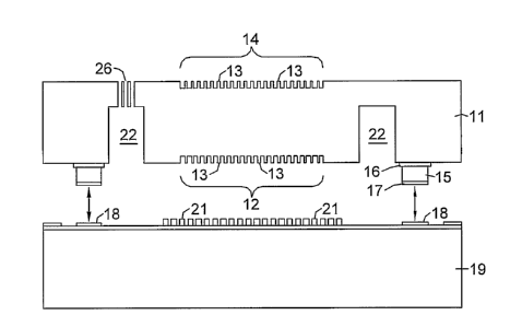
Figure la shows a cross-section view of a topcap
wafer 11. Wafer 11 is a float-zone wafer, i.e., having
low oxygen content and being low-doped. The bottom or
interior surface 29 of wafer 11 may have an
antireflective surface 12. Surface 12 may be bumps 13
etched with a plasma etcher. A stepper may be needed for
printing the bump patterns. Bumps 13 may be smaller than
the wavelength of light that is to pass through wafer 11.
The height or depth 32 of the bumps, posts or pedestals
4

CA 02552250 2006-06-29
WO 2005/067047 PCT/US2004/042583
13 may be approximately X/4. The cross-dimensions or
width 33 of the bumps, posts or pedestals 13 may be from
2/10 to k/5. The indexes of refraction of bumps 13 and
the places of space between the bumps (e.g., air or
vacuum) may be averaged. This average index may be
appropriate for attaining maximum anti-reflective (AR)
properties of surface 12. A plan view of AR surface 12
is shown in Fig. lb.
Interior cavity surface 29 of package cover or wafer
11 also may have an antireflection element, indicated
generally at area 12, extending at least over an area
above the detector pixel 21 array, and preferably over a
greater area of cavity surface 29. Element 12 may be a
field of upstanding posts 13 extending from a ground 34
in the level of surface 29. As an illustrative example,
posts 13 may be shown as right circular cylinders, and
are arranged in a rectangular matrix of rows and columns
in the field of element 12. The dimensions and spacing
(periodicity) of posts 13 may depends upon the refraction
index of the window material and the wavelength band of
the incident radiation desired to be detected. To
approximate a quarter-wavelength antireflective layer 12,
the height or depth 32 of posts 13 may be about
h=k/(4n), where k is the approximate center of the
5

CA 02552250 2006-06-29
WO 2005/067047
PCT/US2004/042583
wavelength band of interest, and n is the effective index
of refraction of the field of element 12. Post height 32
may be typically in the range of 0.2 micron to 4 microns,
corresponding to band centers from 3 to 60 microns. To
avoid reflection at surface 29, it may be desirable to
make n=(n,)1/2, where n, is the index of the solid window
or wafer 11 material. Because posts 13 may be arranged
in a pattern having symmetry in two orthogonal
directions, n could be regarded as isotropic. The
antireflective properties of the field of element 12 may
be then the same for all polarizations of the incident
radiation. The pattern could also have other shapes; for
example, hexagonal posts 13 may permit higher packing
density within the field of element 12.
In this illustrative example, the tops of posts 13
may be flush with interior surface 29 of the cavity, and
their bottoms, the ground level 34, may lie beyond that
surface into wafer 11. Alternatively, posts may be
fabricated as holes extending below interior surface 29,
having substantially the same cross-sectional area as
posts 13. The term "posts" may be used here to denote
both upstanding posts and depressed holes. The shapes of
the posts (or holes) may be round, square, rectangular,
or have any other convenient cross section. It may be
6

CA 02552250 2006-06-29
WO 2005/067047 PCT/US2004/042583
also possible to fabricate posts (or holes) having a non-
vertical sidewalls; that is, the posts can be shaped to
provide a varying cross section along their height, such
as substantially pyramidal or conical, including frustum
and other variations of these shapes where the cross
section decreases along the height of the posts (or,
equivalently, depth of holes). Such posts offer enhanced
antireflection performance over a wider range of
wavelengths.
A desired effective index n of the field of element
12 may depend upon nw and upon the fill factor or relative
area A = Ap/Af of the posts Ap to the total field Af. An
approximate relationship for the effective index may be:
n = [ (1-A+Anw2) (A+ (1-A) nw2) +11,2] / [2 (A+ (1-A) n2)] } 1/2
For round pillars of diameter d and center-to-center
spacing s, A = (n/4)(d/s)2. The relative areas of other
shapes may be calculated. For silicon, the fill factor
may range from about 20 percent to about 60 percent,
being about 40 percent in this example. Post spacing or
periodicity should be less than any wavelength in the
desired band to avoid diffraction and scatter; for a
rectangular array, this may be also the spacing between
adjacent rows and columns. The lowest spacing may be
determined by process limitations rather than by optical
7

CA 02552250 2006-06-29
WO 2005/067047 PCT/US2004/042583
considerations. For a silicon cover 11 and a detector
pixels 21 operating in the wave band of about 6-12
microns, square posts of side 1.5 microns may be spaced
2.3 microns apart.
An exterior anti-reflective bump pattern 14 may be
etched on an opposite side 31 of wafer 11, as shown in
Figures 2a and 2b. Bumps, posts or pedestals 13 of
element 14 may have the same dimensions as those of
element 12. Without elements 12 and 14, the
transmitivity of wafer 11 may be only about 50 percent.
With one of elements 12 and 14, the transmitivity of
wafer 11 may be about 70 percent. With both elements 12
and 14, then the transmitivity of wafer 11 may be 90
percent or greater.
In Figures 3a and 3b, there may be a spacer layer 15
and a malleable layer 17 that are patterned to match a
seal ring 18 of a thin layer of gold on a detector wafer
19, as in Figure 6. Ring 18 may be another material with
the malleability and bonding qualities similar to gold.
Layer 17 is for compensating for flatness differences
between the two wafers being sealed to each other. About
five microns of nickel may be used as spacer layer 15 to
keep anti-reflective surface 12 and the remaining portion
of lower surface 29 of wafer 11 within the perimeter of
8

CA 02552250 2013-05-08
*
seal ring 18 from touching pixels 21 of detector wafer
19. Other material may be used for the spacer layer 15.
There may be a bonding material 16 between metal 15 and
wafer 11. Solder may be used for layer 17. It may be
several microns thick so as to allow the seals of the
wafers 11 and 19 to match up since both wafers might not
have the same flatness relative to each other. Other
materials in lieu of solder may be used for layer 17 of
the seal.
To provide volume within and between wafers 11 and
19, portions 22 may be etched away from wafer 11, as
shown in Figures 4a and 4b. Wafer 11 may be about 500
microns thick at dimension 23. Portions 22 may be about
400 microns deep at dimension 24 leaving about 100
microns of wafer 11 at the top of portion or volume 22.
Establishing volume 22 may involve one or more hour etch
using a Bosch approach.
Volume 22 does not have to encircle the entire wafer
11. Figure 4b shows a plan view of the bottom surface 29
of wafer 11 where volumes 22 are revealed. Portions or
volumes 22 may be interrupted at the corners of wafer 11
with structural support portions 25. At those portions
25, portion or volume 22 is not etched and the thickness
of wafer 11 may remain at about 500 microns. Thus, wafer
9

CA 02552250 2006-06-29
WO 2005/067047 PCT/US2004/042583
11 may provide volume 22 and yet maintain structural
rigidity with portions 25. The deep recess, volume,
trenches, or portions 22 may be etched by DRIE into the
bottom side 29 of topcap wafer 11 to increase vacuum
volume thereby making the device more tolerant of
outgassing within the resulting sealed structure 27
occurring during its lifetime. Mechanical supports 25
may be present so that the middle region in the area of
surface 12 does not appreciably deflect.
Small vent holes 26, which may regarded as pumpout
ports, as shown in Figures 5a and 5b, may be etched from
the top or exterior surface 31 of wafer 11. These ports,
apertures, or holes 26 may provide for the final
outgassing and sealing of structure 27 after wafers 11
and 19 are bonded to each other.
Topcap wafer 11 may be bonded to detector wafer 19
with heat at about 300 degrees C for a period of time
necessary to achieve a satisfactory bond, generally less
than an hour. Then, bonded wafer pair 27 may be baked
out to remove outgas from pair or structure 27. The
temperature during bake-out may be around 250 degrees C
for about eight hours at a pressure of 10-6 Torr in a
sealed vacuum environmental chamber. Holes 26 may be
open during the bake-out. Then structure 27 may be left

CA 02552250 2006-06-29
WO 2005/067047 PCT/US2004/042583
to cool down to room temperature for about 12 hours. In
the meanwhile, the vacuum or pressure of the environment
of structure 27 in the chamber may remain at about 10-6
Torr or less, such as 10-7 Torr. Then, while under this
pressure after cool-down, small vacuum apertures, ports,
holes 26 may be sealed or plugged with a deposited layer
28. The material of layer 28 may be indium or 50 percent
ratio mix of indium and lead. The bonded and sealed
integral topside vacuum package 27 is shown in cross-
sectional and top views in Figures 7a and 7b,
respectively.
Although the invention has been described with
respect to at least one illustrative embodiment, many
variations and modifications will become apparent to
those skilled in the art upon reading the present
specification. It is therefore the intention that the
appended claims be interpreted as broadly as possible in
view of the prior art to include all such variations and
modifications.
11

Representative Drawing
A single figure which represents the drawing illustrating the invention.
Administrative Status

For a clearer understanding of the status of the application/patent presented on this page, the site Disclaimer , as well as the definitions for Patent , Administrative Status , Maintenance Fee  and Payment History  should be consulted.

Administrative Status

Title Date
Forecasted Issue Date 2017-04-04
(86) PCT Filing Date 2004-12-08
(87) PCT Publication Date 2005-07-21
(85) National Entry 2006-06-29
Examination Requested 2006-11-01
(45) Issued 2017-04-04

Abandonment History

Abandonment Date Reason Reinstatement Date
2015-09-30 FAILURE TO PAY FINAL FEE 2015-12-04

Payment History

Fee Type Anniversary Year Due Date Amount Paid Paid Date
Registration of a document - section 124 $100.00 2006-06-29
Application Fee $400.00 2006-06-29
Request for Examination $800.00 2006-11-01
Maintenance Fee - Application - New Act 2 2006-12-08 $100.00 2006-11-09
Maintenance Fee - Application - New Act 3 2007-12-10 $100.00 2007-11-20
Maintenance Fee - Application - New Act 4 2008-12-08 $100.00 2008-10-30
Maintenance Fee - Application - New Act 5 2009-12-08 $200.00 2009-11-10
Maintenance Fee - Application - New Act 6 2010-12-08 $200.00 2010-11-19
Maintenance Fee - Application - New Act 7 2011-12-08 $200.00 2011-11-28
Maintenance Fee - Application - New Act 8 2012-12-10 $200.00 2012-11-15
Maintenance Fee - Application - New Act 9 2013-12-09 $200.00 2013-11-12
Maintenance Fee - Application - New Act 10 2014-12-08 $250.00 2014-11-14
Maintenance Fee - Application - New Act 11 2015-12-08 $250.00 2015-11-20
Reinstatement - Failure to pay final fee $200.00 2015-12-04
Final Fee $300.00 2015-12-04
Maintenance Fee - Application - New Act 12 2016-12-08 $250.00 2016-11-18
Maintenance Fee - Patent - New Act 13 2017-12-08 $250.00 2017-12-04
Maintenance Fee - Patent - New Act 14 2018-12-10 $250.00 2018-11-30
Maintenance Fee - Patent - New Act 15 2019-12-09 $450.00 2019-11-29
Maintenance Fee - Patent - New Act 16 2020-12-08 $450.00 2020-11-24
Maintenance Fee - Patent - New Act 17 2021-12-08 $459.00 2021-11-24
Maintenance Fee - Patent - New Act 18 2022-12-08 $458.08 2022-11-24
Maintenance Fee - Patent - New Act 19 2023-12-08 $473.65 2023-11-24
Owners on Record

Note: Records showing the ownership history in alphabetical order.

Current Owners on Record
HONEYWELL INTERNATIONAL INC.
Past Owners on Record
HIGASHI, ROBERT E.
NEWSTROM-PEITSO, KAREN M.
RIDLEY, JEFFREY A.
Past Owners that do not appear in the "Owners on Record" listing will appear in other documentation within the application.
Documents

To view selected files, please enter reCAPTCHA code :


To view images, click a link in the Document Description column. To download the documents, select one or more checkboxes in the first column and then click the "Download Selected in PDF format (Zip Archive)" or the "Download Selected as Single PDF" button.

List of published and non-published patent-specific documents on the CPD .

If you have any difficulty accessing content, you can call the Client Service Centre at 1-866-997-1936 or send them an e-mail at CIPO Client Service Centre.


Document
Description 
Date
(yyyy-mm-dd) 
Number of pages   Size of Image (KB) 
Abstract 2006-06-29 2 70
Claims 2006-06-29 6 121
Drawings 2006-06-29 5 59
Description 2006-06-29 11 368
Representative Drawing 2006-06-29 1 9
Cover Page 2006-09-08 1 41
Claims 2010-02-24 3 76
Description 2010-02-24 11 359
Description 2011-08-08 11 358
Claims 2011-08-08 3 75
Description 2013-05-08 11 353
Claims 2013-05-08 3 77
Claims 2014-07-02 3 77
Representative Drawing 2015-02-04 1 5
Claims 2015-12-04 5 149
Claims 2016-07-04 5 141
Correspondence 2010-03-02 1 30
PCT 2006-06-29 3 85
Assignment 2006-06-29 3 88
Correspondence 2006-09-05 1 27
Prosecution-Amendment 2006-11-01 1 40
Assignment 2007-02-13 7 265
Prosecution-Amendment 2009-09-02 3 82
Prosecution-Amendment 2010-02-24 11 424
Prosecution-Amendment 2011-08-08 17 640
Prosecution-Amendment 2011-02-08 4 165
Prosecution-Amendment 2012-11-08 4 170
Prosecution-Amendment 2013-05-08 10 386
Prosecution-Amendment 2013-08-16 3 101
Prosecution-Amendment 2014-01-03 4 142
Prosecution-Amendment 2014-07-02 8 300
Amendment 2015-12-04 7 203
Correspondence 2015-12-04 2 55
Examiner Requisition 2016-01-06 4 254
Amendment 2016-07-04 11 380
Office Letter 2017-02-28 1 44
Cover Page 2017-03-01 1 40