Note: Descriptions are shown in the official language in which they were submitted.
CA 02552511 2006-07-04
WO 2005/067683 PCT/US2005/000075
INORGANIC NANOWIRES
This application claims benefit under 35 U.S.C. ~ 119(e) to provisional
application no.
60/534,102 filed January 5, 2004 by Belcher et al., which is hereby
incorporated by reference in
its entirety.
This work was supported by the National Science Foundation through NIRT, grant
no.
the Army Research Office, grant no. ; and the Air Force
Scientific Research Office, grant no. . The government may have
rights in the invention.
INTRODUCTION
The reliance of a wide variety of technologies on developing scalable and
economic
methods for the fabrication of one-dimensional materials, including nanowires
and nanotulies,
has spurred intense and rapid progress in the area of materials synthesis. For
example, one-
dimensional materials have been enthusiastically pursued for their
applications in the study of,
for example, electrical transport (1), optical phenomena (2), and as
functional units in
nanocircuitry (3). Pursuit of "bottom up" methods for the synthesis of
semiconducting, metallic
and magnetic nanowires has yielded a variety of synthetic strategies
including, but not limited to,
Vapor Liquid Solid (VLS) (4), chemical (5), solvothermal, vapor phase, and
template-directed
fabrication (6). Although each method developed for the production of
nanowires has had some
basic success in achieving high quality materials, methods to date have not
yielded
monodisperse, crystalline nanowires of radically different compositions. In
general, prior
methods for nanowire production can be erratic, synthetically cumbersome, and
are not
universal. See, for example, U.S. Patent No. 6,225,198 to Alivisatos et al.
for II-VI
semiconductor production in liquid media and references cited herein.
Reference 4 to Lieber et
al. describes the difficulty in fording a universal approach. It describes a
VLS process that
requires use of lasers and high temperatures and produces a nanowire having a
nanoparticle at
the end .which may not be desirable.
Recently, biological factors have been exploited as synthesis directors for
nanofibers (7,
8), virus-based particle cages (9), virus-particle assemblies (10, 11, 12),
and non-specific peptide
templates (13). This is due to the high degree of organization, ease of
chemical modification and
naturally occurring self assembly motifs in these systems.
CA 02552511 2006-07-04
WO 2005/067683 PCT/US2005/000075
Belcher et al. have prepared nanowires associated with and bound to
genetically
engineered viral scaffolds (see, for example, U.S. Patent Publication,
2003/0068900 to Belcher et
al.). The scaffolds serve as a template as nanoparticles or nanocrystals form
on the scaffold.
Although this technology is attractive and provides important advantages, a
need exists to
improve upon it. For example, it is desirable to generate improved properties
such as improved
fusion between the nanocrystals and reduction in defects. It is also desirable
to fuse the
nanocrystals into one long single crystal rod or into large crystalline
domains. Moreover, it is
desirable in many applications to not have and substantially eliminate the
viral scaffold bound to
or associated with the viral scaffold. Moreover, it is desirable to control
the size and size
statistical distributions for the nanowires including, for example, prepare
monodisperse materials
and materials having controlled length. If possible, the nanowires should be
usable directly,
without need for a size-based separation step before use: A need also exists
to be able to connect
the nanowires with other components such as electrodes which allow the
nanowires to be
commercially useful. These connections should, if possible, not be mere chance
connections but
be strategically directed and controllable.
References numerically cited in this specification are provided in a listing
at the end of
the specification and are incorporated by reference in the specification in
their entirety.
SUm~IMARY
The present invention in many of its embodiments is summarized in this non-
limiting
summary section.
In one embodiment, the present invention provides an inorganic nanowire having
an
organic scaffold substantially removed from the inorganic nanowire, the
inorganic nanowire
consisting essentially of fused inorganic nanoparticles substantially free of
the organic scaffold
("the inorganic nanowire of embodiment I ").
The present invention also provides compositions and devices comprising a
plurality of
these inorganic nanowires. In another embodiment, the present invention
provides a composition
comprising a plurality of inorganic nanowires, wherein the inorganic nanowires
comprise fused
inorganic nanoparticles substantially free of organic scaffold.
In another embodiment, the present invention provides a method of forming an
inorganic
nanowire comprising the steps of (1) providing one or more precursor materials
for the
2
CA 02552511 2006-07-04
WO 2005/067683 PCT/US2005/000075
inorganic nanowire; (2) providing an elongated organic scaffold; (3) reacting
the one or more
precursor materials in the presence of the scaffold to form nanoparticles,
wherein the
nanoparticles are disposed along the length of the elongated organic scaffold;
and (4) thermally
treating the scaffold and the nanoparticles to form the inorganic nanowire by
fusion of the
nanoparticles. In some embodiments, the organic scaffold can be removed, such
as during the
thermal treatment. The present invention also provides nanowires prepared by
this method.
Also provided is a method of forming an inorganic nanowire comprising the
steps of (1)
providing one or more precursor materials for the inorganic nanowire; (2)
providing an organic
scaffold; (3) reacting the one or more precursor materials in the presence of
the scaffold under
conditions to form the inorganic nanowire. In some embodiments, the organic
scaffold can be
removed, such as during the reacting. The present invention also provides
nanowires prepared
by this method.
The present invention also provides for use'of a filamentous organic scaffold
as a
sacrificial organic scaffold in the production of an inorganic nanowire
comprising providing a
filamentous organic scaffold and an inorganic nanowire precursor on the
scaffold, converting the
inorganic nanowire precursor to the inorganic nanowire while removing the
filamentous organic
scaffold to yield the inorganic nanowire.
An additional use provided herein is the use of an elongated organic scaffold
to control
the length of an inorganic nanowire disposed thereon, comprising the step of
genetically
engineering the scaffold to control the length of the scaffold.
An important embodiment is also a device comprising an electrode in electrical
contact
with the inorganic nanowire of embodiment 1 or any other nanowire described
herein. In
another embodiment, the device can further comprise at least two electrodes
each in electrical
contact with the inorganic nanowire of embodiment 1 or any other nanowire
described herein.
Examples of devices include a field effect transistor or a sensor. In other
embodiments; the
device comprises at least two nanowires according to embodiment 1, or any
other nanowires
described herein, wherein the nanowires are in a parallel arrangement, or in a
crossed
arrangement.
The invention also provides a segmented nanowire comprising a plurality of
connected
segments of inorganic nanowires of embodiment 1 or any other nanowires
described herein. In
CA 02552511 2006-07-04
WO 2005/067683 PCT/US2005/000075
some embodiments, the scaffold was used to form the nanowire and/or direct the
placement of
the nanowire before being removed.
The invention also provides a composition comprising a plurality of inorganic
nanowires,
wherein the inorganic nanowires comprise fused inorganic nanoparticles that
were disposed on
an organic scaffold. In some embodiments, the scaffolds) were used to form the
nanowires
and/or direct the placement of the nanowires, such as placement in a circuit
substrate, before
being removed.
The invention also provides a process for producing nanowires with use of an
elongated
organic scaffold comprising the steps of: (1) providing an elongated organic
scaffold which
comprises a plurality of binding sites including binding sites along the
length of the scaffold and
binding sites on at least one end of the scaffold; (2) disposing a nanowire
precursor composition
along the length of the scaffold to form a scaffolded precursor composition;
and (3) treating the
scaffolded precursor composition to form the nanowire. In some embodiments,
the scaffold is
substantially removed, such as during the treating step. In one embodiment,
the elongated
organic scaffold has binding sites at both ends of the scaffold. In another
embodiment, the
process further comprises the step of using the binding site at the end of the
scaffold to bind to
another structure. For example, the another structure can be another elongated
organic scaffold.
The invention also provides compositions. For example, in one embodiment, a
nanowire
composition is provided comprising a nanowire with a thermodynamically high
energy phase, or
a collection of nanowires according to this embodiment, wherein the nanowires
are substantially
monodisperse in length, width, or length and width. In this embodiment, the
nanowire can be an
inorganic nanowire such as, for example, a nanowire of semiconductive
material, metallic
material, metal oxide material, magnetic material, or mixtures thereof.
The invention also provides an inorganic nanowire comprising fused inorganic
nanoparticles, or a composition comprising a collection of inorganic nanowires
according to this
embodiment. In this embodiment, the invention also provides an inorganic
nanowire comprising
fused inorganic nanoparticles comprising semiconductor material, metallic
material, metal oxide
material, or magnetic material, as well as collections of these nanowires.
The invention also provides an inorganic nanowire consisting essentially of
fused
inorganic nanoparticles that were disposed on an organic scaffold.
4
CA 02552511 2006-07-04
WO 2005/067683 PCT/US2005/000075
A basic and novel feature for many embodiments of the present invention is the
substantial elimination of the organic scaffold when it is used to prepare the
nanowire. In many
embodiments, its preferred that the organic scaffold be totally eliminated.
Moreover, a basic and
novel advantage in many embodiments is that the nanowires can be fabricated
directly with good
monodispersity without use of a size-based separation of some nanowires from
other nanowires.
Additional enumerated embodiments are provided. A first aspect (1) is, for
example, an
inorganic nanowire having an organic scaffold substantially removed from the
inorganic
nanowire, the inorganic nanowire consisting essentially of fused inorganic
nanoparticles
substantially free of the organic scaffold.
2. The inorganic nanowire according to 1, wherein the inorganic nanowire is
crystalline.
3. The inorganic nanowire according to 2, wherein the crystallographic axis of
the
nanoparticles is oriented with respect to the surface of the scaffold.
4. The inorganic nanowire according to 1, wherein the inorganic nanowire is a
single
crystalline domain.
5. The inorganic nanowire according to 1, wherein the inorganic nanowire has
one or
more crystalline domains.
6. The inorganic nanowire according to 1, wherein the fused nanoparticles are
single
crystalline.
7. The inorganic nanowire according to 1, wherein the inorganic nanowire
consists
essentially of semiconductor material, metallic material, metal oxide
material, magnetic material,
or mixtures thereof.
8. The inorganic nanowire according to 1, wherein the nanowire consists
essentially of
semiconductor material.
9. The inorganic nanowire according to 1, wherein the nanowire consists
essentially of
metallic material.
10. The inorganic nanowire according to 1, wherein the nanowire consists
essentially of
metal oxide material.
11. The inorganic nanowire according to 1, wherein the nanowire consists
essentially of
magnetic material.
12. The inorganic nanowire according to 1, wherein the nanowire has a length
of about
250 nm to about 5 microns and a width of about 5 nm to about 50 nm.
S
CA 02552511 2006-07-04
WO 2005/067683 PCT/US2005/000075
13. The inorganic nanowire according to l, wherein the nanowire has a length
of about
400 nm to about one micron and a width of about 10 nm to about 30 nm.
14. The inorganic nanowire according to 1, wherein the nanowire consists
essentially of
semiconductor material, and the nanowire has a length of about 250 nm to about
five microns
and a width of about 5 nm to about 50 nm.
15. The inorganic nanowire according to 1, wherein the nanowire consists
essentially of
II-VI semiconducting material and has a length of about 250 nm to about five
microns and a
width of about 5 nm to about 50 nm.
16. The inorganic nanowire according to 1, wherein the nanowire is
substantially
straight.
17. The inorganic nanowire according to 1, wherein the nanowire consists
essentially of
semiconductor material and is substantially straight.
18. The inorganic nanowire according to 1, wherein the nanowire consists
essentially of
a thermodynamically high energy phase.
19. The inorganic nanowire according to 1, wherein the inorganic nanowire is
crystalline
and the inorganic nanowire consists essentially of semiconductor material,
metallic material,
metal oxide material, magnetic material, or mixtures thereof.
20. The inorganic nanowire according to 19, wherein the inorganic nanowire is
single
crystalline.
21. The inorganic nanowire according to 19, where the fused nanoparticles are
single
crystalline.
22. The inorganic nanowire according to 19, wherein the nanowire is
substantially
straight.
23. The inorganic nanowire according to 19, wherein the nanowire has a length
of about
250 nm to about 5 microns and a width of about 5 nm to about 50 nm.
24. The inorganic nanowire according to 19, wherein the nanowire has a length
of about
400 nm to about one micron and a width of about 10 nm to about 30 nm.
25. The inorganic nanowire according to 23, wherein the nanowire is
substantially
straight.
26. The inorganic nanowire according to 24, wherein the nanowire is
substantially
straight.
6
CA 02552511 2006-07-04
WO 2005/067683 PCT/US2005/000075
27. A composition comprising a plurality of inorganic nanowires according to
1, wherein
the nanowires are substantially monodisperse in average length.
28. A composition comprising a plurality of inorganic nanowires according to
1, wherein
the nanowires are substantially monodisperse in average width.
29. A composition comprising a plurality of inorganic nanowires according to
1, wherein
the nanowires are substantially monodisperse in average length, and are also
substantially
monodisperse in average width.
30. The composition according to 29, wherein nanowires have a coefficient of
variation
for length of less than 10% and a coefficient of variation for width of less
than 10%.
31. The composition according to 29, wherein nanowires have a coefficient of
variation
for length of less than 5% and a coefficient of variation for width of less
than 5%.
32. A composition comprising a plurality of inorganic nanowires according to
19,
wherein the nanowires are substantially monodisperse in average length.
33. A composition comprising a plurality of inorganic nanowires according to
19,
wherein the nanowires are substantially monodisperse in average width.
34. A composition comprising a plurality of inorganic nanowires according to
19,
wherein the nanowires are substantially monodisperse in average length, and
are also
substantially monodisperse in average width.
A thirtyfifth (35) aspect is a composition comprising a plurality of inorganic
nanowires,
wherein the inorganic nanowires comprise fused inorganic nanoparticles
substantially free of
organic scaffold.
36. The composition according to 35, wherein the inorganic nanowires are
crystalline.
37. The composition according to 36, wherein the crystallographic axis of the
nanoparticles is oriented with respect to the surface of the scaffold.
38. The composition according to 35, wherein individual inorganic nanowires
comprise a
single crystalline domain.
39. The composition according to 35, wherein individual inorganic nanowires
have one
or more crystalline domains.
40. The composition according to 35, wherein the fused nanoparticles are
single
crystalline.
7
CA 02552511 2006-07-04
WO 2005/067683 PCT/US2005/000075
41. The composition according to 35, wherein the inorganic nanowires comprise
semiconductor material, metallic material, metal oxide material, magnetic
material, or mixtures
thereof.
42. The composition according to 35, wherein the nanowires comprise
semiconductor
material.
43. The composition according to 35, wherein the nanowires comprise metallic
material.
44. The composition according to 35, wherein the nanowires comprise metal
oxide
material.
45. The composition according to 35, wherein the nanowires comprise magnetic
material.
46. The composition according to 35, wherein the nanowires have an average
length of
about 250 nm to about 5 microns and an average width of about 5 nm to about 50
nm.
47. The composition according to 35, wherein the nanowires have an average
length of
about 400 nm to about one micron and an average width of about 10 nm to about
30 nm.
48. The composition according to 35, wherein the nanowires comprise
semiconductor
material, and the nanowires have an average length of about 250 nm to about
five microns and an
average width of about 5 nm to about 50 nm.
49. The composition according to 35, wherein the nanowires comprise II-VI
semiconducting material and have an average length of about 250 nm to about
five microns and
an average width of about 5 nm to about 50 nm.
50. The composition according to 35, wherein the nanowires are substantially
straight.
51. The composition according to 35, wherein the nanowires are substantially
monodisperse in width.
52. The composition according to 35, wherein the nanowires are substantially
monodisperse in length.
53. The composition according to 35, wherein the nanovvires are substantially
monodisperse in width and length.
54. The composition according to 53, wherein nanowires have a coefficient of
variation
for length of less than 10% and a coefficient of variation for width of less
than 10%.
55. The composition according to 53, wherein nanowires have a coefficient of
variation
for length of less than 5% and a coefficient of variation for width of less
than 5%.
8
CA 02552511 2006-07-04
WO 2005/067683 PCT/US2005/000075
A fifty-sixth aspect (56) is a method of forming an inorganic nanowire
comprising the
steps of (1) providing one or more precursor materials for the inorganic
nanowire; (2) providing
an elongated organic scaffold; (3) reacting the one or more precursor
materials in the presence of
the scaffold to form nanoparticles, wherein the nanoparticles are disposed
along the length of the
elongated organic scaffold; and (4) thermally treating the scaffold and the
nanoparticles to form
the inorganic nanowire by fusion of the nanoparticles.
57. The method according to 56, wherein the organic scaffold is substantially
removed
from the nanowire.
58. The method according to 57, wherein the scaffold is removed during the
thermal
treatment step.
59. The method according to 56, wherein the nanoparticles are crystalline.
60. The method according to 56, wherein the precursor materials are a
precursor to
semiconductor material, metallic material, metal oxide material, magnetic
material.
61. The method according to 56, wherein the precursor materials are a
precursor to
semiconductor material.
62. The method according to 56, wherein the precursor materials are a
precursor to
metallic material.
63 The method according to 56, wherein the precursor materials are a precursor
to metal
oxide material.
64. The method according to 56, wherein the precursor materials are a
precursor to
magnetic material.
65. The method according to 56, wherein the elongated organic scaffold is a
viral
scaffold.
66. The method according to 56, wherein the elongated organic scaffold is a
filamentous
viral scaffold.
67. The method according to 56, wherein the elongated organic scaffold
comprises
surface peptides along the length of the scaffold which bind to the
nanoparticles.
68. The method according to 56, wherein the thermally treating step is carried
out at
about 100°C to about 1,000°C.
69. The method according to 56, wherein the thermally treating step is earned
out at
about 300°C to about 500°C.
9
CA 02552511 2006-07-04
WO 2005/067683 PCT/US2005/000075
70. The method according to 56, wherein the nanoparticles have an average
diameter of
about 2 nm to about 10 nm.
71. The method according to 56, wherein the nanoparticles have an average
diameter of
about 3 nm to about 5 nm.
72. The method according to 56, wherein the nanowire is crystalline.
73. The method according to 56, wherein the nanowire is a single crystalline
domain.
74. The method according to 56, wherein the nanowire has one or more
crystalline
domains.
75. The method according to 56, wherein the nanowire comprises a
thermodynamically
high energy phase.
76. The method according to 56, wherein the thermal treating step coverts the
nanowire
from a polycrystalline state to a single crystalline state.
77. The method according to 56, wherein the crystallographic axis of the
nanoparticles is
oriented with respect to the surface of the scaffold.
78. The method according to 56, wherein the nanoparticles are not fused before
the
thermally treating step.
79. The method according to 56, wherein the nanowire is substantially
straight.
80. The method according to 56, wherein the method is used to prepare a
plurality of
nanowires and the nanowires are substantially monodisperse in length.
81. The method according to 56, wherein the method is used to prepare a
plurality of
nanowires and the nanowires are substantially monodisperse in width.
82. The method according to 56, wherein the method is used to prepare a
plurality of
nanowires and the nanowires are substantially monodisperse in width and
length.
83. The method according to 56, wherein the precursor materials are a
precursor to
semiconductor material, metallic material, metal oxide material, magnetic
material, and the
nanowire is crystalline and substantially straight.
84. The method according to 83, wherein the method is used to prepare a
plurality of
nanowires and the nanowires are substantially monodisperse in length.
85. The method according to 83, wherein the method is used to prepare a
plurality of
nanowires and the nanowires are substantially monodisperse in width.
CA 02552511 2006-07-04
WO 2005/067683 PCT/US2005/000075
86. The method according to 83, wherein the method is used to prepare a
plurality of
nanowires and the nanowires are substantially monodisperse in width and
length.
87. The method according to 86, wherein nanowires have a coefficient of
variation for
length of less than 10% and a coefficient of variation for width of less than
10%.
88. The composition according to 86, wherein nanowires have a coefficient of
variation
for length of less than 5% and a coefficient of variation for width of less
than 5%.
89. A method of forming an inorganic nanowire comprising the steps of: (1)
providing
one or more precursor materials for the inorganic nanowire; (2) providing an
organic scaffold;
(3) reacting the one or more precursor materials in the presence of the
scaffold under conditions
to form the inorganic nanowire.
90. The method according to 89, wherein the organic scaffold is substantially
removed
from the nanowire.
91. The method according to 89, wherein the organic scaffold is removed during
the
reacting step.
92. The method according to 89, wherein the precursor materials are
nanoparticles or
form nanoparticles.
93. The method according to 92, wherein the nanoparticles are crystalline.
94. The method according to 92, wherein the crystallographic axis of the
nanoparticles is
oriented with respect to the surface of the scaffold.
95. The method according to 89, wherein the precursor materials are a
precursor to
semiconductor material, metallic material, metal oxide material, magnetic
material.
96. The method according to 89, wherein the precursor materials are a-
precursor to
semiconductor material.
97. The method according to 89, wherein the precursor materials are a
precursor to
metallic material.
98. The method according to 89, wherein the precursor materials are a
precursor to metal
oxide material.
99. The method according to 89, wherein the precursor materials are a
precursor to
magnetic material.
100. The method according to 89, wherein the organic scaffold is a viral
scaffold.
11
CA 02552511 2006-07-04
WO 2005/067683 PCT/US2005/000075
101. The method according to 89, wherein the organic scaffold is a filamentous
viral
scaffold.
102. The method according to 89, wherein the elongated organic scaffold
comprises
surface peptides along the length of the scaffold which bind to the nanowire.
103. The method according to 89, wherein the reacting step is carried out with
use of
temperature between about 100°C to about 1,000°C to form the
nanowire.
104. The method according to 89, wherein the nanowire is crystalline.
105. The method according to 89, wherein the nanowire is a single crystalline
domain.
106. The method according to 89, wherein the nanowire has one or more
crystalline
domains.
107. The method according to 89, wherein the nanowire is substantially
straight.
108. The method according to 89, wherein the method is used to prepare a
plurality of
nanowires and the nanowires are substantially monodisperse in length.
109. The method according to 89, wherein the method is used to prepare a
plurality of
nanowires and the nanowires are substantially monodisperse in width.
110. The method according to 89, wherein the method is used to prepare a
plurality of
nanowires and the nanowires are substantially monodisperse in width and
length.
111. The method according to 110, wherein nanowires have a coefficient of
variation for
length of less than 10% and a coefficient of variation for width of less than
10%.
112. The composition according to 110, wherein nanowires have a coefficient of
variation for length of less than 5% and a coefficient of variation for width
of less than 5%.
113. The method according to 89, wherein the precursor materials are a
precursor to
semiconductor material, metallic material, metal oxide material, magnetic
material, and the
nanowire is crystalline and substantially straight.
114. The method according to 113, wherein the method is used to prepare a
plurality of
nanowires and the nanowires are substantially monodisperse in length.
115. The method according to 113, wherein the method is used to prepare a
plurality of
nanowires and the nanowires are substantially monodisperse in width.
116. The method according to 1 I3, wherein the method is used to prepare a
plurality of
nanowires and the nanowires are substantially monodisperse in width and
length.
12
CA 02552511 2006-07-04
WO 2005/067683 PCT/US2005/000075
117. Use of a filamentous virus as a sacrificial organic scaffold in the
production of an
inorganic nanowire comprising providing a filamentous virus scaffold and an
inorganic nanowire
precursor on the scaffold, and removing the filamentous virus scaffold to
yield the inorganic
nanowire.
118. Nanowire prepared by the method of 56.
119. Nanowire prepared by the method of 89.
Another aspect (120) is use of a filamentous organic scaffold as a sacrificial
organic
scaffold in the production of an inorganic nanowire comprising providing a
filamentous organic
scaffold and an inorganic nanowire precursor on the scaffold, converting the
inorganic nanowire
precursor to the inorganic nanowire while removing the filamentous organic
scaffold to yield the
inorganic nanowire.
Another aspect (121) is use of an elongated organic scaffold to control the
length of an
inorganic nanowire disposed thereon, comprising the step of genetically
engineering the scaffold
to control the length of the scaffold.
122. A device comprising an electrode in electrical contact with a nanowire
according to
1.
123. The device according to 122, wherein the device comprises at least two
electrodes
each in electrical contact with the nanowire according to 1.
124. The device according to 122, wherein the device is field effect
transistor.
125. The device according to 122, wherein the device is a sensor.
126. A device comprising at least two nanowires according to 1, wherein the
nanowires
are in a parallel arrangement.
127. A device comprising at least two nanowires according to 1, wherein the
nanowires
are in a crossed arrangement.
128. A segmented nanowire comprising a plurality of connected segments of
nanowires
according to 1.
Another aspect (129) is a process for producing nanowire with use of an
elongated
organic scaffold comprising the steps of:
providing an elongated organic scaffold which comprises a plurality of binding
sites
including binding sites along the length of the scaffold and binding sites on
at least one end of
the scaffold;
13
CA 02552511 2006-07-04
WO 2005/067683 PCT/US2005/000075
disposing a nanowire precursor composition along the length of the scaffold to
form a
scaffolded precursor composition;
treating the scaffolded precursor composition to form the nanowire.
130. The process according to 129, wherein the organic scaffold is
substantially removed
from the nanowires.
131. The process according to 129, wherein the organic scaffold is removed
during the
treating step.
132. The process according to 129, wherein the elongated organic scaffold has
binding
sites at both ends of the scaffold.
133. The process according to 129, further comprising the step of using the
binding site
at the end of the scaffold to bind to another structure.
134. The process according to 133, wherein the another structure is another
elongated
organic scaffold.
135. The process according to 129, wherein the another structure is a circuit
element or
an electrode.
136. The process according to 129, further comprising the step of binding the
scaffold to
a patterned structure before its removal.
137. A nanowire composition comprising a nanowire with a thermodynamically
high
energy phase.
138. A collection of nanowires according to 137, wherein the nanowires are
substantially
monodisperse in length.
139. A collection of nanowires according to 137, wherein the nanowires are
substantially
monodisperse in width.
140. A collection of nanowires according to 137, wherein the nanowires are
substantially
monodisperse in length and width.
141. The collection according to 140, wherein nanowires have a coefficient of
variation
for length of less than 10% and a coefficient of variation for width of less
than 10%.
142. The composition according to 140, wherein nanowires have a coefficient of
variation for length of less than 5% and a coefficient of variation for width
of less than 5%.
143. A nanowire composition according to 137, wherein the nanowire is an
inorganic
nanowire.
14
CA 02552511 2006-07-04
WO 2005/067683 PCT/US2005/000075
144. A nanowire composition according to 137, wherein the nanowire is a
nanowire of
semiconductive material, metallic material, metal oxide material, magnetic
material, or mixtures
thereof.
145. A nanowire composition according to 137, wherein the nanowire is a
nanowire of
semiconductive material.
146. A nanowire composition according to 137, wherein the nanowire is a
nanowire of
metallic material.
147. A nanowire composition according to 137, wherein the nanowire is a
nanowire of
metal oxide material.
148. A nanowire composition according to 137, wherein the nanowire is a
nanowire of
magnetic material.
149. An inorganic nanowire comprising fused inorganic nanoparticles.
150. A composition comprising a collection of inorganic nanowires according to
149.
151. An inorganic nanowire comprising fused inorganic nanoparticles comprising
semiconductor material.
152. A composition comprising a collection of inorganic nanowires according to
151.
153. An inorganic nanowire comprising fused inorganic nanoparticles comprising
metallic material.
154. A composition comprising a collection of inorganic nanowires according to
153.
155. An inorganic nanowire comprising fused inorganic nanoparticles comprising
metal
oxide material.
156. A composition comprising a collection of inorganic nanowires according to
155.
157. An inorganic nanowire comprising fused inorganic nanoparticles comprising
magnetic material.
158. A composition comprising a collection of inorganic nanowires according to
157.
159. An inorganic nanowire comprising fused inorganic nanoparticles disposed
on an
organic scaffold.
160. The inorganic nanowire according to 159, wherein the inorganic nanowire
is
crystalline.
161. The inorganic nanowire according to 160, wherein the crystallographic
axis of the
nanoparticles is oriented with respect to the surface of the scaffold.
CA 02552511 2006-07-04
WO 2005/067683 PCT/US2005/000075
162. The inorganic nanowire according to 159, wherein the inorganic nanowire
is a
single crystalline domain.
163. The inorganic nanowire according to 159, wherein the inorganic nanowire
has one
or more crystalline domains.
164. The inorganic nanowire according to 159, wherein the fused nanoparticles
are
single crystalline.
165. The inorganic nanowire according to 159, wherein the inorganic nanowire
consists
essentially of semiconductor material, metallic material, metal oxide
material, magnetic material,
or mixtures thereof.
166. The inorganic nanowire according to 159, wherein the nanowire has a
length of
about 250 nm to about 5 microns and a width of about 5 nm to about 50 nm.
167. The inorganic nanowire according to 159, wherein the nanowire has a
length of
about 400 nm to about one micron and a width of about 10 nm to about 30 nm.
168. The inorganic nanowire according to 159, wherein the nanowire consists
essentially
of semiconductor material, and the nanowire has a length of about 250 nm to
about five microns
and a width of about 5 nm to about 50 run.
169. The inorganic nanowire according to 159, wherein the nanowire comprises
II-VI
semiconducting material and has a length of about 250 nm to about five microns
and a width of
about 5 nm to about 50 nm.
170. The inorganic nanowire according to 159, wherein the nanowire is
substantially
straight.
171. The inorganic nanowire according to 159, wherein the nanowire comprises
semiconductor material and is substantially straight.
172. The inorganic nanowire according to 159, wherein the nanowire comprises a
thermodynamically high energy phase.
173. The inorganic nanowire according to 159, wherein the inorganic nanowire
is
crystalline and the inorganic nanowire comprises semiconductor material,
metallic material,
metal oxide material, magnetic material, or mixtures thereof.
174. The inorganic nanowire according to 173, wherein the .inorganic nanowire
is single
crystalline.
16
CA 02552511 2006-07-04
WO 2005/067683 PCT/US2005/000075
175. The inorganic nanowire according to 173, where the fused nanoparticles
are single
crystalline.
176. The inorganic nanowire according to 173, wherein the nanowire is
substantially
straight.
177. The inorganic nanowire according to 173, wherein the nanowire has a
length of
about 250 nm to about 5 microns and a width of about 5 nm to about 50 nm.
178. The inorganic nanowire according to 173, wherein the nanowire has a
length of
about 400 nm to about one micron and a width of about 10 nm to about 30 nm.
179. The inorganic nanowire according to 177, wherein the nanowire is
substantially
straight.
180. The inorganic nanowire according to claim 178, wherein the nanowire is
substantially straight.
181. A composition comprising a plurality of inorganic nanowires according to
claim
159 herein the nanowires are substantially monodisperse in average length.
182. A composition comprising a plurality of inorganic nanowires according to
claim
159, wherein the nanowires are substantially monodisperse in average width.
183. A composition comprising a plurality of inorganic nanowires according to
claim
159, wherein the nanowires are substantially monodisperse in average length,
and are also
substantially monodisperse iri average width.
184. The composition according to claim 183, wherein nanowires have a
coefficient of
variation for length of less than 10% and a coefficient of variation for width
of less than 10%.
185. The composition according to claim 183, wherein nanowires have a coeff
cient of
variation for length of less than 5% and a coefficient of variation for width
of less than 5%.
186. A composition comprising a plurality of inorganic nanowires according to
claim
173, wherein the nanowires are substantially monodisperse in average length.
187. A composition comprising a plurality of inorganic nanowires according to
claim
173, wherein the nanowires are substantially monodisperse in average width.
188. A composition comprising a plurality of inorganic nanowires according to
claim
173, wherein the nanowires are substantially monodisperse in average length,
and are also
substantially monodisperse in average width.
17
CA 02552511 2006-07-04
WO 2005/067683 PCT/US2005/000075
189. A composition comprising a plurality of inorganic nanowires, wherein the
inorganic
nanowires comprise fused inorganic nanoparticles disposed on an organic
scaffold.
190. The composition according to 189, wherein the inorganic nanowires are
crystalline.
191. The composition according to 190, wherein the crystallographic axis of
the
nanoparticles is oriented with respect to the surface of the scaffold.
192. The composition according to I89, wherein individual inorganic nanowires
comprise a single crystalline domain.
193. The composition according to 189, wherein individual inorganic nanowires
have
one or more crystalline domains.
194. The composition according to 189, wherein the fused nanoparticles are
single
crystalline.
195. The composition according to 189, wherein the inorganic nanowires
comprise
semiconductor material, metallic material, metal oxide material, magnetic
material, or mixtures
thereof.
196. The composition according to 189, wherein the nanowires have an average
length
of about 250 nm to about 5 microns and an average width of about 5 nm to about
50 nm.
197. The composition according to 189, wherein the nanowires have an average
length
of about 400 nm to about one micron and an average width of about 10 nm to
about 30 nm.
198. The composition according to 189, wherein the nanowires comprise
semiconductor
material, and the nanowires have an average length of about 250 nm to about
five microns and an
average width of about S nm to about 50 nm.
199. The composition according to 189, wherein the nanowires comprise II-VI
semiconducting material and have an average length of about 250 run to about
five microns and
an average width of about 5 nm to about 50 nm.
200. The composition according to 189, wherein the nanowires are substantially
straight.
201. The composition according to 189, wherein the nanowires are substantially
monodisperse in width.
202. The composition according to 189, wherein the nanowires are substantially
monodisperse in length.
203. The composition according to 189, wherein the nanowires are substantially
monodisperse in width and length.
18
CA 02552511 2006-07-04
WO 2005/067683 PCT/US2005/000075
204. The composition according to 203, wherein nanowires have a coefficient of
variation for length of less than 10% and a coefficient of variation for width
of less than 10%.
205. The composition according to 203, wherein nanowires have a coefficient of
variation for length of less than 5% and a coefficient of variation for width
of less than 5%.
BRIEF DESCRIPTION OF DRAWINGS
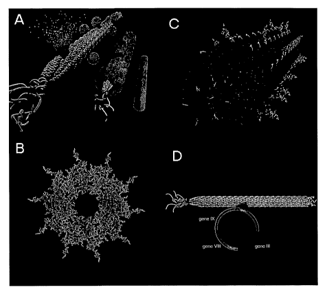
Figures lA-D illustrate viruses which can be used as scaffolds.
Figures 2A-F provide characterization of nanowires made of semiconductor
material.
Figures 3A-F provide characterization of nanowires made of magnetic material.
DETAILED DESCRIPTION
I. Introduction
The present invention provides, in one embodiment, an inorganic nanowire
having an
organic scaffold substantially removed from the inorganic nanowire, the
inorganic nanowire
consisting essentially of fused inorganic nanoparticles substantially free of
the organic scaffold.
The present invention also provides compositions comprising a plurality of
these inorganic
nanowires. This invention also provides compositions comprising a plurality of
inorganic
nanowires, wherein the inorganic nanowires comprise fused inorganic
nanoparticles substantially
free of organic scaffold.
The organic scaffold is generally removed so that, preferably, it cannot be
detected on the
nanowire. This substantial removal can be described in terms of weight
percentage remaining.
For example, the amount of remaining organic scaffold with respect to the
total amount of
nanowire and scaffold can be less than 1 wt.%, more preferably, less than 0.5
wt.%, and more
preferably, less than 0.1 wt.%. A basic and novel feature of the invention is
the substantial
removal of the scaffold in the production of high quality nanowires.
In another patent application, which is hereby incorporated by reference in
its entirety,
[U.5. serial no. 10/665,721 filed September 22, 2003 to Belcher et al.
("Peptide Mediated
Synthesis of Metallic and Magnetic Materials")], additional description is
provided for burning
off and elimination of a viral scaffold from materials to which the scaffold
can selectively bind.
In this application, annealing temperatures of 500-1,000°C are
described for burning off the
scaffold. In addition, Mao et al., Virus-based toolkit for the directed
synthesis of magnetic and
19
CA 02552511 2006-07-04
WO 2005/067683 PCT/US2005/000075
semiconducting nanowires, Science 303:213-217 (2004), which is hereby
incorporated by
reference including all figures and the experimental section, includes some
teachings that may be
useful in practicing the present invention. Fairley, Peter, (2003) Germs That
Build Circuits,
IEEE Spectrum 37-41, which is hereby incorporated by reference in its entirety
including all
figures and use of electrodes connected by. nanowires, also includes teachings
that may be useful
in practicing the present invention, such as applications of nanowires.
Priority provisional
application no. 60/534,102 filed January 5, 2004 by Belcher et al., is hereby
incorporated by
reference in its entirety.
The detailed description of the invention is organized according to the
following sections:
(1) introduction, (2) scaffold which is substantially removed, (3) nanowires,
(4) methods of
making nanowires, (5) applications for the nanowires, and (6) working
examples.
II. Scaffold
Although the scaffold ultimately may be substantially removed from the
nanowire, the
scaffold is an important part of the invention. In the practice of the present
invention, one skilled
in the art can refer to technical literature for guidance on how to design and
synthesize the
scaffold including the literature cited herein and listed at the conclusion of
the specification. For
example, although the present invention relates to organic scaffolds and is
not limited only to
viral scaffolds in its broadest scope, viral scaffolds are a preferred
embodiment. In particular, an
elongated organic scaffold can be used which is a virus, and the term virus
can include both a
full virus and a virus subunit such as a capsid. The literature describes the
preparation of viral
scaffolds through genetic engineering with recognition properties for
exploitation in materials
synthesis. This includes use of viruses in the production of inorganic
materials which have
technologically useful properties and nanoscopic dimensions. In the present
invention, one
skilled in the art can use the literature in the practice of the present
invention to prepare inorganic
nanowires on scaffolds, wherein the scaffolds are later substantially
eliminated so that the
inorganic nanowire is substantially free of the scaffold. When the scaffold is
intended to be
removed, the scaffold may be referred to as a "sacrificial scaffold."
One skilled in the art, for example, can refer to the following patent
literature for
selection of the virus, genetic engineering methods, and for materials to be
used with genetically
engineered viruses. Phage display libraries and experimental methods for using
them in
CA 02552511 2006-07-04
WO 2005/067683 PCT/US2005/000075
biopanning are further described, for example, in the following U.S. patent
publications to
Belcher et al.: ( 1 ) "Biological Control of Nanoparticle Nucleation, Shape,
and Crystal Phase";
2003/0068900 published April 10, 2003; (2) "Nanoscale Ordering of Hybrid
Materials Using
Genetically Engineered Mesoscale Virus"; 2003/0073104 published April 17,
2003; (3)
"Biological Control of Nanoparticles"; 2003/0113714 published June 19, 2003;
and (4)
"Molecular Recognition of Materials"; 2003/0148380 published August 7, 2003,
which are each
hereby incorporated by reference in their entirety. Additional patent
applications useful for one
skilled in the art describe viral and peptide recognition studies with use of
genetically engineered
viruses for materials synthesis and applications including, for example, (1)
U.S. serial no.
10/654,623 filed September 4, 2003 to Belcher et al. ("Compositions, Methods,
and Use of Bi-
Functional BioMaterials"), (2) U.S, serial no. 10/665,721 filed September 22,
2003 to Belcher et
al. ("Peptide Mediated Synthesis of Metallic and Magnetic Materials"), and (3)
U.S. serial no.
10/668,600 filed September 24, 2003 to Belcher et al. ("Fabricated BioFilm
Storage Device"),
(4) U.S. provisional ser. No. 60/510,862 filed October 15, 2003 and the U.S.
utility application
ser. No. 10/965,665 filed October 15, 2004 to Belcher et al. ("Viral Fibers"),
and (5) U.S.
provisional ser. No. 60/511,102 filed October 15, 2003 and the U.S. utility
application ser. No.
filed October 15, 2004 to Belcher et al. ("Multifunctional Biomaterials...");
each of
which are hereby incorporated by reference. These references describe a
variety of specific
binding modifications which can be carried out for binding to conjugate
structures, as well as
forming the conjugate structures in the presence of the material modified for
specific binding. In
particular, polypeptide and amino acid oligomeric sequences can be expressed
on the surfaces of
viral particles, including both at the ends and along the length of the
elongated virus particle such
as M13 bacteriophage, including pIII and pVIII expressions, as well as pIX,
pVII, and pVI
expressions, and combinations thereof. Using these expression sites, the
viruses may be
engineered to express surface peptides along the length of the virus, at the
ends of the virus, or
any number of other sites and combinations of sites. A single site for
modification can be
modified with more than one unit for specific binding. For example, a pVIII
site can be
modified to have two distinctly different binding units. In addition,
different sites for
modification can be modified with the same or different units for binding. For
example, the ends
of the virus particles can be modified to bind to specifically bind a first
material, while the body
of the virus particles can be modified to bind a second material. Multiple
binding sites can be
21
CA 02552511 2006-07-04
WO 2005/067683 PCT/US2005/000075
used to create multifunctional scaffolds that can be used to form nanowires
with specifically
engineered and varying compositions among other applications. The binding
sites can be
designed so that nanoparticles nucleate at the binding sites or the binding
sites can be designed to
bind preformed nanoparticles. The scaffold can be functionalized with
sufficient binding units to
achieve the desired concentration needed to form the nanowire.
In addition, the paper "Selection of Peptides with Semiconductor Binding
Specificity for
Directed Nanocrystal Assembly"; Whaley et al., Nature, Vol. 405, June 8, 2000,
pages 665-668,
herein incorporated by reference, describes a method of selecting peptides
with binding
specificity using a combinatorial library. Specifically, the article shows a
method of selecting
peptides with binding specificity to semiconductor materials using a
combinatorial library with
about 109 different peptides. The combinatorial library of random peptides,
each containing 12
amino acids, were fused to the pIII coat protein of M13 coliphage and exposed
to crystalline
semiconductor structures. Peptides that bound to the semiconductor materials
were eluted,
amplified, and re-exposed to the semiconductor materials under more stringent
conditions. After
the fifth round of selection, the semiconductor specific phages were isolated
and sequenced to
determine the binding peptide. In this manner, peptides were selected with
high binding
specificity depending on the crystallographic structure and composition of the
semiconductor
material. The technique can be modified to obtain peptides with a binding
specificity for not just
semiconductor materials, but a range of both organic and inorganic materials.
One skilled in the art can also refer to, for example, C.E. Flynn et al. Acta
Materialia, vol
13, 2413-2421 (2003) entitled "Viruses as vehicles for growth, organization,
and assembly of
materials." This reference, as well as all references cited therein, are
incorporated herein by
reference in their entirety. In addition, reference 12 below (Mao et al.,
PNAS) is hereby
incorporated by reference for all of its teachings including the nucleation
and structures shown in
Figure 1. Also, in particular, reference 17 (Flynn et al., J. Mater. Chem) is
also incorporated by
reference in its entirety including descriptions of using aqueous salt
compositions to nucleate
nanocrystals which are directed in their crystal structure and orientation by
the recognition sites.
In the present invention, these nucleated nanocrystals can be converted to
single crystalline and
polycrystalline nanowires, wherein the scaffold is substantially removed.
The scaffold is further described including the role of genetic programming
for the
preferred embodiments. Although the viral scaffolds represent a preferred
embodiment, the
22
CA 02552511 2006-07-04
WO 2005/067683 PCT/US2005/000075
present invention comprises other types of non-viral scaffolds as well. Also,
although M13 virus
is a preferred embodiment for a scaffold, the present invention is not limited
to this virus.
The scaffold can comprise an entire virus, a virion, or viral subunits
including capsids.
Viral subunits including proteins, peptides, nucleic acids, DNA, RNA, and the
like, in various
combinations. The scaffold does not require that both peptide and nucleic acid
be present. For
example, virus mimics can be used or engineered, wherein the size, shape, or
structure mimics
that of a virus, but the does not contain nucleic acid and/or may not have the
ability to infect a
host for replication. One skilled in the art can prepare viral scaffolds based
on purely synthetic
methods from the bottom up as well as using more traditional methods wherein
materials are
supplied by nature without or without modification by man.
In a preferred embodiment, wherein the scaffold is a virus or a virus subunit,
the scaffold
is tailored and designed in structure and function by genetic programming
and/or genetic
engineering for production of the one dimensional materials such as nanowires.
The genetic
programming can be used to tailor the scaffold for the particular application,
and applications are
described further below. The references in Section I describe genetic
programming which is
further described in this section for use in practice of the present
invention. See, e.g.,
Genetically Engineered Viruses, Christopher Ring and E.D. Blair (Eds.), Bios
Scientific, 2001,
for descriptions of developments and applications in use of viruses as
vehicles and expressors of
genetic material including, for example, prokaryotic viruses, insect viruses,
plant viruses, animal
DNA viruses, and animal RNA viruses. In the present invention, genetic
programming can be
carried out to engineer a scaffold using the different displayed peptide
features of a virus such as,
for example, a filamentous bacteriophage such as, for example, the M13 virus
which has a rod
shape. Genetic programming can be used to control the scaffold for materials
synthesis, the viral
scaffold comprising one or more viral particle subunits which may or may not
include the
nucleic acid subunit of the virus. Also, the scaffold may or may not retain
infectability.
An overall commercial advantage to this genetic programming approach to
materials
engineering, in addition to materials-specific addressability, is the
potential to specify viral
length and geometry. For example, an elongated organic scaffold may be
genetically engineered
to control the length of the scaffold. This engineering of length can allow
the design of
nanowires of specific, controlled lengths, for example. Hence, a variety of
methods can be used
to control the scaffold length and geometry.
23
CA 02552511 2006-07-04
WO 2005/067683 PCT/US2005/000075
For example, the length of a filamentous virus is generally related to the
size of its
packaged genetic information and the electrostatic balance between the pVIII-
derived core of the
virion and the DNA. See, e.g., B. K. Kay, J. Winter, J. McCafferty, Phage
Display of Peptides
and Proteins: A Laboratory Manual, Academic Press, San Diego, 1996; Greenwood
et al.,
Journal of Molecular Biology 217:223-227 (1992). Phage observed by AFM
generally are seen
to be roughly 860 nm and as short as 560 nm depending on whether the complete
M13 genome
or smaller phagemid are used in sample preparation. See, e.g., reference 12,
C. Mao, C. E.
Flynn, A. Hayhurst, R. Sweeney, J. Qi, J. Williams, G. Georgiou, B. Iverson,
A. M. Belcher,
Proc. Natl. Acad. Sci. 2003, 100, 6946. Also, changing a single lysine to
glutamine on the inner-
end of pVIII can result in particles approximately 35% longer than wild type
phage. See, e.g., J.
Greenwood, G . J. Hunter, R. N. Perham, J. Mol. Biol. 1991, 217, 223.
In addition, specific linkage, binding, and concatenation of virus particles
can help
produce longer viral scaffolds, and thus longer nanowires. The multiplicity of
additions can be
controlled by engineering binding motifs into one virus, which then can
accurately recognize
binding sites on another virus. For example, the pIII protein resides at one
end of the M13 virus
and can be exploited to display peptide and protein fusions. At the other end
of the virus, the
pIX and pVII proteins also can be subject to modification. For example, Gao
and coworkers
utilized pIX and pVII fusions to display antibody heavy- and light-chain
variable regions.[ See,
e.g., C. Gao, S. Mao, G. Kaufmann, P. Wirsching, R. A. Lerner, K. D. Janda,
Proc. Natl. Acad.
Sci. 2002, 99, 12612] See, also, for example, U.S. Patent No. 6,472,147 for
genetic
modification of viruses. These end modifications may be used to link the virus
particles directly
or the end modifications may specifically bind to a linker. The linker may be
any suitable
material. For example, the linker can be a nanoparticle, amino acid oligomer,
nucleic acid
oligomer, or a polymer. This present invention encompasses dual-end viral
display, either for
generating bimodal heterostructures, or in combination with pVIII, producing
end-functionalized
nanowires.
In addition, dual-end directional linkages enable creation of other
interesting and
commercially useful geometries, such as rings, squares and other arrays. The
binding of one end
of a virus directly to the other end of the virus without the use. of a linker
can be used to form
rings, wires, or other viral based structures as well. By engineering
recognition sites and the
24
CA 02552511 2006-07-04
WO 2005/067683 PCT/US2005/000075
corresponding conjugate moieties into a single virus, or multiple viruses, the
entire system can be
genetically programmed.
An important advantage of the invention is that.the organic scaffold can be an
active
scaffold, wherein the scaffold not only serves as a template for synthesis of
the inorganic
nanowire, but also actively assists in coupling the inorganic nanowire to
other structures. For
example, an organic scaffold which is designed at one end to bind to another
structure can be
used to couple the inorganic nanowire to the structure. The scaffolds and the
nanowires can be
coupled to each other, for example, to form segments of similar or dissimilar
materials. In this
embodiment, the composition of the nanowire would vary as a function of
length.
Additional description is provided for the types of viral structures which can
be designed
by genetic programming for particular applications based on length control,
geometry control,
binding control, and the like. The virus scaffold is not particularly limited,
and combinations of
viruses can be used of different types. In general, viruses can be used which
can be
multifunctionalized. In general, virus particles which are long, filamentous
structures can be
used. See, e.g., Genetically Engineered Viruses, Christopher Ring (Ed.), Bios
Scientif c, 2001,
pages 11-21. Additionally, other viral geometries such as dodecahedral and
icosahedral can be
multifunctionalized and used to create composite materials. Virus particles
which can function
as flexible rods, forming liquid crystalline and otherwise aligned structures,
can be used.
In particular, phage display libraries, directed evolution, and biopanning are
an important
part of genetic programming of viruses, and viruses can be used which have
been subjected to
biopanning in the viral design so that the virus particles specifically can
recognize and bind to
materials which were the object of the biopanning. The materials can also be
nucleated and
synthesized in particulate form, including nanoparticulate form, in the
presence of the specific
recognition and binding sites. Use of filamentous virus in so called directed
evolution or
biopanning is further described in the patent literature including, for
example, U.S. Patent Nos.
5,223,409 and 5,571,698 to Ladner et al. ("Directed Evolution of Novel Binding
Proteins").
Additional references on the recognition properties of viruses include U.S.
Patent No. 5,403,484
(phage display libraries, now commercially available) and WO 03/078451.
Mixtures of two or more different kinds of viruses can be used. Mixtures of
virus
particles with non-virus materials can be used in forming materials which use
the present
invention.
CA 02552511 2006-07-04
WO 2005/067683 PCT/US2005/000075
Virus and virus particle can include both an entire virus and portions of a
virus including
at least the virus capsid. The term virus can refer to both viruses and
phages. Entire viruses can
include a nucleic acid genome, a capsid, and may optionally include an
envelope. Viruses as
described in the present invention may further include both native and
heterologous amino acid
oligomers, such as cell adhesion factors. The nucleic acid genome may be
either a native
genome or an engineered genome. A virus particle further includes portions of
viruses
comprising at least the capsid.
In general, a virus particle has a native structure, wherein the peptide and
nucleic acid
portions of the virus are arranged in particular geometries, which are sought
to be preserved
when it is incorporated in solid state, self supporting forms such as films
and fibers.
Viruses are preferred which have expressed peptides, including peptide
oligomers and
amino acid oligomer as specific binding sites. Amino acid oligomers can
include any sequence
of amino acids whether native to a virus or heterologous. Amino acid oligomers
may be any
length and may include non-amino acid components. Oligomers having about 5 to
about 100,
and more particularly, about 5 to about 30 amino acid units as specific
binding site can be used.
Non-amino acid components include, but are not limited to sugars, lipids, or
inorganic
molecules.
The size and dimensions of the virus particle can be such that the particle is
anisotropic
and elongated. Generally, the viruses may be characterized by an aspect ratio
of at least 25, at
least 50, at least 75, at least 100, or even at least 250 or 500 (length to
width, e.g, 25:1 ).
A wide variety of viruses may be used to practice the present invention. The
compositions and materials of the invention may comprise a plurality of
viruses of a single type
or a plurality of different types of viruses. Preferably, the virus particles
comprising the present
invention are helical viruses. Examples of helical viruses include, but are
not limited to, tobacco -.
mosaic virus (TMV), phage pfl, phage fdl, CTX phage, and phage M13. These
viruses are
generally rod-shaped and may be rigid or flexible. One of skill in the art may
select viruses
depending on the intended use and properties of the virus.
Preferably, the viruses of the present invention have been engineered to
express one or
more peptide sequences including amino acid oligomers on the surface of the
viruses. The
amino acid oligomers may be native to the virus or heterologous sequences
derived from other
organisms or engineered to meet specific needs.
26
CA 02552511 2006-07-04
WO 2005/067683 PCT/US2005/000075
A number of references teach the engineering of viruses to express amino acid
oligomers
and may be used to assist in practicing the present invention. For example,
U.S. Patent No.
5,403,484 by Ladner et al discloses the selection and expression of
heterologous binding
domains on the surface of viruses. U.5. Patent No. 5,766,905 by Studier et al
discloses a display
vector comprising DNA encoding at least a portion of capsid protein followed
by a cloning site
for insertion of a foreign DNA sequence. The compositions described are useful
in producing a
virus displaying a protein or peptide of interest. U.5. Patent No. 5,885,808
by Spooner et al
discloses an adenovirus and method of modifying an adenovirus with a modified
cell-binding
moiety. U.S. Patent No. 6,261,554 by Valerio et al shows an engineered gene
delivery vehicle
comprising a gene of interest and a viral capsid or envelope carrying a member
of a specific
binding pair. U.5. Published Patent Application 2001/0019820 by Li shows
viruses engineered
to express ligands on their surfaces for the detection of molecules, such as
polypeptides, cells,
receptors, and channel proteins.
The genetically engineeredwiruses can be prepared by methods and vectors as
described
in Kay, B. K.; Winter, J.; McCafferty, J. Phage Display of Peptides and
Proteins: A Laboratory
Manual; Academic Press: San Diego, 1996, and in particular, chapter 3,
"Vectors for Phage
Display" and references cited therein. In addition, the genetically engineered
viruses can be
prepared by methods as described in, Phage Display, A Laboratory Manual, by
Barbas et al.
(2001) including Chapter 2, "Phage Display Vectors" and references cited
therein. The type of
vector is not particularly limited. Table 2.1 of Barbas provides exemplary
vectors which can be
used in various combinations to provide the multifunctional viruses. For
example, type 3, type
8+8, and phagemid type p7/p9 can be combined. Or type 8 and type 3 can be
combined along
with phagemid p7/p9 as desired. One skilled in the art can develop other
combinations based on
particular applications. Methods can be developed to either display the
peptide on some or
substantially all copies of the coat protein.
M13 systems are a preferred example of a filamentous virus scaffold, but other
types of
filamentous virus scaffolds can be used as well. The wild type filamentous
M1.3 virus is
approximately 6.5 nm in diameter and 880 nm in length. The length of the
cylinder reflects the
length of the packaged single stranded DNA genome size. At one end of M13
virus, there are
approximately five molecules each of protein VII (pVII) and protein IX (pIX).
The other end
has about five molecules each of protein III (pIII) and protein VI (pVI),
totaling 10-16 nm in
27
CA 02552511 2006-07-04
WO 2005/067683 PCT/US2005/000075
length. The wild type M13 virus coat is composed of roughly 2800 copies of the
major coat
protein VIII (pVIII) stacked in units of 5 in a helical array.
In sum, evolution of substrate specific peptides through phage display
technologies for
the directed nucleation of materials on the nanometer scale has been
previously reported by
papers and patents from Angela Belcher and coworkers (see above description)
and serves as the
basis for the material specificity in the virus scaffold or template (16) of
the present invention.
Screening phage libraries for the ability to nucleate and assemble inorganic
systems including,
for example, the ZnS, CdS (12, 17), Feet and Copt systems (18) using
commercially available
bacteriophage libraries expressing either a disulphide constrained
heptapeptide or a linear
dodecapeptide, has yielded the consensus sequences CNNPMHQNC (termed A7; ZnS),
SLTPLTTSHLRS (termed J140; CdS), HNKHLPSTQPLA (termed FP12; FePt), and
ACNAGDHANC (termed CP7; CoPt). Incorporation of these peptides into the highly
ordered,
.self assembled capsid of the M13 bacteriophage virus provides a linear
template which can
simultaneously control particle phase and composition, while maintaining an
ease of material
adaptability through genetic tuning of the basic protein building blocks.
Because the protein
sequences responsible for the materials growth are gene linked and contained
within the capsid
of the virus, exact genetic copies of this scaffold are relatively easily
reproduced by infection
into a large suspension of bacterial hosts.
To prepare nanowires, an anisotropic scaffold can be used which has the
ability to collect
nanoparticles being formed around it and locate them on the scaffold for
fusion into a nanowire.
In this invention, an inorganic nanowire composition can be formed having a
scaffold
substantially removed from the inorganic nanowire. Non-viral scaffolds can
also be used
including, for example, a variety of other organic scaffolds including, for
example, scaffolds
which have peptide or protein recognition units as side groups on an organic
backbone. For
example, the organic backbone can be a synthetic polymer backbone, which are
well known in
the art. For example, polymer scaffolds can be used including for example
modified
polystyrenes of uniform molecular weight distribution which are functionalized
with peptide
units. Another example is branched polypeptides or nucleic acids which are
modified to have
recognition sites. Another example is a nanolithographically printed peptide
structures such as a
line with nanoscale width. In general, DNA, proteins, and polypeptides can be
modified with
recognition units, including peptide recognition units, to function as the
organic scaffold.
28
CA 02552511 2006-07-04
WO 2005/067683 PCT/US2005/000075
Suitable recognition units include, but are not limited to, amino acid
oligomers, nucleic acid
oligomers, polymers, organic molecules (e.g., antibodies, antigens, cell
adhesion factors, and
trophic factors), and inorganic materials.
In one embodiment, scaffolds and virus particles can be used which are not
directly
genetically engineered. However, in general, desirable properties can be
achieved when the
virus is genetically engineered or genetic engineering is used in designing
the scaffold.
III. Nanowires
Using methods described in the previous sections, viruses can be genetically
engineered
so that they function as a scaffold and bind to conjugate moieties in an
overall process which
ultimately yields a production of inorganic nanowires according to the present
invention. For
example, a rod-shaped virus can direct the synthesis of nanoparticulates
materials along the
length of the rod, and these nanoparticulates materials can be fused into
nanowires.
In the present invention, the conjugate materials can be inorganic materials
which form
nanoparticles including inorganic nanocrystals. From these inorganic
nanoparticles, inorganic
nanowires can be formed consisting essentially of the fused inorganic
nanoparticles upon
substantial removal of the scaffold. T'he conjugate materials and the
inorganic nanowires can
consist essentially of technologically useful materials such as, for example,
semiconducting
materials, whether doped or undoped; metallic materials; metal oxide
materials, and magnetic
materials. Various oxide materials including silica and alumina fall within
the scope of the
invention. Additional materials of interest for nanotechnology commercial
applications are
further described in, for example: (a) Understanding Nanotechnology, Warner
Books, 2002,
including materials for circuits such as nanowires and nanotubes described in
the chapter "The
Incredible Shrinking Circuit", pgs. 92-103 by C. Lieber. (b) Made to Measure,
New Materials
for the 21st Century, Philip Ball, Princeton University, (c) Introduction to
Nanotechnology, C.P.
Poole Jr., F. J. Owens, Wiley, 2003. Preferably, for nanowires, the materials
prepared on the
scaffold conduct electricity as an electrical conductor, are semiconductive
(whether inherently or
via doping), transmit light, are magnetic, or possess some other
technologically useful property.
Other properties include ferroelectric, piezoelectric, converse-piezoelectric,
and thermoelectric).
Semiconductors are a particularly important type of inorganic nanowire
material. The
semiconductor material can be, for example, any of the standard types
including alloys thereof
29
CA 02552511 2006-07-04
WO 2005/067683 PCT/US2005/000075
including IV-IV Group (e.g., Si, Ge, Si~~_X~GeX), III-V Group binary (e.g.,
GaN, GaP), III-V
Group ternary (e.g., Ga(Asl_XPX)), II-VI Group binary (e.g., ZnS, ZnSe, CdS,
CdSe, CdTe), IV-
VI Group binary (e.g., PbSe), transition metal oxides (e.g., BiTi03), and
combinations thereof.
Magnetic materials can be those known in the art including nanostructured
magnetic
materials. See, for example, Introduction to Nanotechnology, C.P. Poole Jr.,
F. J. Owens, Wiley,
2003, Chapter 7, pages 165-193 ("Nanostructured Ferromagnetism) and references
cited therein
(see, e.g., page 193).
In general, although the present invention is not limited by theory, the
nanowires can be
structures wherein the nanoparticles form into nanowires and collapse into a
fused structure at
the end of the process. The porosity of the nanowire is not particularly
limited, but in general,
non-porous nanowire materials are preferred, particularly for conductive
applications wherein
porosity could interfere with desired conductivity. Alternatively, the
nanowire can be porous.
The nanowire can be crystalline. The nanowire can be a single crystalline
domain or can
have one or more crystalline domains. In one embodiment, the fused
nanoparticles are single
crystalline. The crystalline phase can be either the thermodynamically
favorable crystalline state
or a crystalline state which is not thermodynamically favorable but is locked
in by the relative
orientation of the crystalline nanoparticles before fusion. The nanoparticles
can be oriented in
any manner. For example, the crystallographic axis of the nanoparticles can be
oriented with
respect to the surface of the scaffold.. One can vary the thermal treatment in
the method of
making (see below) to achieve a desired crystalline structure, or to covert
polycrystalline
structures to single crystalline structures. One can also vary the thermal
treatment to remove the
organic scaffold. In some cases fusion and organic scaffold removal are
achieved at the same
temperature, in other cases, fusion can occur before removal.
The length of the nanowire can be, for example, about 250 nm to about 5
microns, or
more particularly, about 400 nm to about 1 micron.
The width of the nanowire can be, for example, about S nm to about 50 nm, or
more
particularly, about 10 nm to about 30 nm.
In some embodiments, the length of the nanowire can be, for example, about 250
nm to
about 5 microns, and have a width, for example, of about 5 nm to about SO nm.
In other
embodiments, the length of the nanowire can be, for example, about 5 nm to
about 50 nm, and
have a width, for example, of about 10 nm to about 30 nm.
CA 02552511 2006-07-04
WO 2005/067683 PCT/US2005/000075
When a plurality of nanowires is present, the lengths and widths can be
expressed as
average lengths and widths using known statistical methods in materials
science. For example,
the average length of the nanowire can be, for example, about 250 nm to about
5 microns, or
more particularly, about 400 nm to about 1 micron. The average width of the
nanowire can be,
for example, about 5 nm to about 50 nm, or more particularly, about 10 nm to
about 30 nm.
Also, when a plurality of nanowires is present, the nanowires can be
substantially
monodisperse in length and/or width. The monodispersity can be accomplished,
because the
nanowires are assembled from scaffolds with uniform length and width. Again,
known statistical
methods in material science can be used to calculate the polydispersity for
length and width. For
example, images of the nanowires can be obtained and, for example, 20-50
nanowires can be
selected for statistical analysis. The coefficient of variation (CV) can be
calculated wherein the
standard deviation is divided by the mean. The CV can be, for example, less
than about 20%,
more preferably, less than about 10%, more preferably, less than about 5%, and
more preferably,
less than about 3%.
The nanowires can be substantially straight. For example, straightness can be
estimated
by (1) measuring the true length of the nanowire, (2) measuring the actual end
to end length, (3)
calculate the -ratio of true length to actual end to end length. For a
perfectly straight nanowire,
this ratio will be one. In the invention, ratios close to one can be achieved
including, for
example, less than 1.5, less than 1.2, and less than 1.1.
The inorganic nanowires of the present invention can also be formed in
combination with
other types of conjugate materials to form larger structures using, for
example, multifunctional
scaffolds. Hence, the conjugate material is not particularly limited to
inorganic materials for
these larger structures and combinations of materials can be used. In general,
it will be selected
for a particular application. It can be selected so that the virus particles
can be subjected to
biopanning against the conjugate material, and then the conjugate material is
selectively or
specifically bound to the virus particle. In some applications, selective
binding can be
sufficient, whereas in other applications, a more powerful specific binding
can be preferred.
Examples of general types of conjugate materials which can be used in larger
structures include
inorganic, organic, particulate, nanoparticulate, single crystalline,
polycrystalline, amorphous,
metallic, magnetic, semiconductor, polymeric, electronically conducting,
optically active,
conducting polymeric, light-emitting, and fluorescent materials. Conjugate
materials are
31
CA 02552511 2006-07-04
WO 2005/067683 PCT/US2005/000075
described further, for example, in the patent publications and technical
literature to Angela
Belcher and co-workers cited throughout this specification.
In sum, the present invention relates to the general, universal synthesis of 1-
D
nanostructures, including nanowires, based on, in preferred embodiments, a
genetically modified
virus scaffold for the directed growth and assembly of crystalline
nanoparticles into 1-D arrays,
followed by annealing of the virus-particle assemblies into high aspect ratio,
crystalline
nanowires through oriented, aggregation-based crystal growth (14, 15) (FIG.
2A). The synthesis
of analogous nanowire structures from fundamentally different materials, e.g.,
the II-VI
semiconductors ZnS and CdS and the Llo ferromagnetic alloys Copt and Feet,
demonstrates
both the generality of the virus scaffold and the ability to precisely control
material
characteristics through genetic modification. In contrast to other synthetic
methods (6), this
approach allows for the genetic control of crystalline semiconducting,
metallic, oxide, and
magnetic materials with a universal scaffold template.
IV. Method of Making Inorganic Nanowires
The present invention also provides methods of making the inorganic nanowires,
which
are further exemplified in the below working examples. For example, the
invention provides a
method of forming an inorganic nanowire comprising the steps.of (1) providing
one or more
precursor materials for the inorganic nanowire; (2) providing an elongated
organic scaffold; (3)
reacting the one or more precursor materials in the presence of the scaffold
to form
nanoparticles, wherein the nanoparticles are disposed along the length of the
elongated organic
scaffold; and (4) thermally treating the scaffold and the nanoparticles to
form the inorganic
nanowire by fusion of the nanoparticles. In some embodiments, the thermal
treatment is not
performed, and the method comprises the steps listed as (1)-(3) above. This
method of forming a
nanowire can also be used to form a plurality of nanowires.
In these methods, the inorganic nanowires are described in the previous
section including
the crystallinity, types of materials, size including length and width,
monodispersity, and
straightness. Also, in these methods, the elongated organic scaffold is
described above including
the viral system with its potential for selective recognition. These methods
include situations
involving the substantial removal of the organic scaffold.
32
CA 02552511 2006-07-04
WO 2005/067683 PCT/US2005/000075
The invention is not particularly limited by the type of reaction and the
precursor
materials used to form the nanowire. In general, the reaction and the
precursor materials should
be compatible with the scaffold. Reactions at temperatures of below
100°C can be used to form
the nanoparticles. In a preferred embodiment, the treating step comprises a
chemical reduction
of metal precursor salts. Precursor material can be preformed nanoparticles or
materials that
form nanoparticles, for example.
In a preferred embodiment, the nanoparticles can have an average diameter of
about 2 nm
to about 10 nm, and more particularly, about 3 nm to about 5 nm. The
nanoparticles can be
crystalline before and/or after the thermal treating. The nanoparticles can be
fused before and/or
after thermal treatment. For example, the thermal treatment may act to fuse
the nanoparticles,
which were not fused prior to the thermal treatment. The nanoparticles can be
oriented or not
oriented.
The temperature and time of the thermal treatment step are not particularly
limited but
can vary depending on the precursor materials used and the material of the
final nanowire. For
example, the melting temperatures and annealing behavior of the materials can
be considered in
selecting temperature. In general, temperatures of about 100°C to about
1,000°C can be used.
Thermal treatment can be used to fuse the nanoparticles into a single
structure and also to
remove the scaffold, tailored for a particular application with particular
materials. In principle,
the porosity of the nanowire and the degree of fusion of the nanoparticles can
be affected by the
temperature. In a preferred embodiment, the thermal treatment step can be
carried out at about
300°C or higher, up to about 500°C. In general, and depending on
the materials, lower
temperatures can be used such as, for example, about 200°C to about
300°C if more porous
nanowires are desired with less fusion. The thermal treatment step can be
carried out at a
temperature below the melting temperature of the precursor material. The
temperature can be
selected to achieve a desired crystalline phase which may be a low energy
phase or a high energy
phase. If desired, a temperature programming step can be used to tailor the
fusion of the
nanoparticles, the targeted crystal phase, and the removal of the scaffold, if
desired. Higher
temperatures of, for example, about 500°C to about 1,000°C can
be used to ensure the scaffold is
completely removed and burned off. Lower temperatures, for example, about
50°C to 300°C,
can be used to avoid removing the scaffold. However, temperature and time can
be selected so
as to not result in excessive oxidation of the nanowires. The time of the
thermal treatment is not
33
CA 02552511 2006-07-04
WO 2005/067683 PCT/US2005/000075
particularly limited but can be, for example, 30 minutes to 12 hours.
Preferably, the temperature
and time for thermal treatment can be adjusted to achieve the optimum balance
for nanoparticle
fusion while reducing oxide.formation and improving the stability of the
crystal structure.
In one embodiment, the invention provides a process for producing nanowires
with use of
an elongated organic scaffold comprising the steps of: (1) providing an
elongated organic
scaffold which comprises a plurality of binding sites including binding sites
along the length of
the scaffold and binding sites on at least one end of the scaffold; (2)
disposing a nanowire
precursor composition along the length of the scaffold to form a scaffolded
precursor
composition; and (3) treating the scaffolded precursor composition to form the
nanowire. In one
embodiment, the elongated organic scaffold has binding sites at both ends of
the scaffold. In
another embodiment, the process further comprises the step of using the
binding site at the end of
the scaffold to bind to another structure. The other structure can be, for
example, another
elongated organic scaffold. an electrode, a circuit element, a semiconductor
material, an
electrically conductive material, a magnetic material, or a biological
molecule. The scaffold can
be bound to a patterned structure, such as a circuit substrate. The treating
step may be a thermal
treatment step as described in detail herein. The scaffold can be removed or
left intact.
V. Applications
The nanowires of the present invention can be used in many different
commercial
applications, some of which are noted above, including the cited patent
applications, and in the
cited references at the end of the specification. The nanowires can be used,
for example, in
applications requiring electrical conductivity or semiconductivity at the
nanoscale. The large
surface area to volume ratio of nanowires is advantageous for applications,
such as, fuel cells,
thin film batteries, and supercapacitors. In some applications, a single
nanowire can be used. In
other applications, a plurality of nanowires can be used, whether in a
parallel or crossed manner.
In general, organized arrangements of nanowires are advantageous. In some
applications, the
nanowire can be surface modified, doped, or otherwise modified in its material
structure for the
application. Modifications include both chemical and biological modifications.
Microcircuitry,
nanocircuitry, macroelectronics, photovoltaics, solar cells, chemical and
biological sensors,
optical components, field emitting tips and devices, nanocomputing,
nanoswitches, molecular
wire crossbars, batteries, fuel cells, catalysts, very large flat panel
displays, tiny radio frequency
identification devices, smart cards, phased array RF antennas, disposable
computing and storage
34
CA 02552511 2006-07-04
WO 2005/067683 PCT/US2005/000075
electronics, nanoscale bar codes, cross bar nanostructures, biosensor arrays,
high density data
storage, field effect transistors, and the like are representative examples of
applications for the
nanowires. Particularly important semiconductive elements include, for
example, p-n diodes, p-
in diodes, LEDs, and bipolar transistors. Nanowires can be incorporated into a
number of
devices, such as electronic, optoelectronic, electrochemical, and
electromechanical devices. A
single nanowire can connect elements in a device or a series of connected
segments of nanowires
can connect elements. For example, a field effect transistor device may
comprise nanowires in
both a parallel and crossed arrangement.
Applications of nanowires are described in, for example, U.S. patent
application
publication no. 2003/0089899 (published May 15, 2003) to Lieber et al. and
include, for
example, field effect transistors, sensors, and logic gates, and this
publication is hereby
incorporated by reference in its entirety including its description of devices
made from
nanowires. Additional applications of nanowires are described in, for example,
U.S. patent
application publication no. 2003/0200521 (published October 23, 2003) to
Lieber et al. and
include nanoscale crosspoints, which is incorporated by reference in its
entirety. Additional
applications of nanowires are described in, for example, U.S. patent
application publication no.
2002/0130353 (published September 19, 2002) to Lieber et al. and include
devices with chemical
patterning and bistable devices. Additional applications of nanowires are
described in, for
example, U.S. patent application publication no. 2002/0117659 (published
August 29, 2002) to
Lieber et al. and include nanosensors for chemical and biological detection.
In addition,
applications for related nanorods are described in, for example, U.S. Patent
Nos. 6,190,634;
6,159,742; 6,036,774; 5,997,832; and 5,897,945 to Lieber et al. A number of
literature
references teach applications of nanowires and related technology, such as
Choi et al., J. Power
Sources 124:420 (2003); Cui et al., Science 293:1289-1292 (2001); De Heeret
al., Science
270:1179-1180 (1995); and Dominko et al., Advanced Materials 14(21):1531-1534
(2002),
which all of which are herein incorporated by reference in their entirety.
Of particular importance for this invention, the scaffold can be used to
direct the
nanowire to other structures so the scaffold is an active scaffold rather than
a passive scaffold.
For example, viruses can be conjugated with one-dimensional
nanowires/nanotubes, two
dimensional nano electrodes, and microscale bulk devices. One-dimensional
materials, such as
nanotubes or nanowires, when conjugated with the pIII end of M13 viruses, may
form phase
CA 02552511 2006-07-04
WO 2005/067683 PCT/US2005/000075
separated lamellar structures that have inorganic nanotube or nanowire layers
and phage building
block layers. Two-dimensional nano-thick plate shaped electrodes can be
organized. Viral-
semiconductor composite nanowires can be attached across metal electrodes,
including noble
metal electrodes such as gold electrodes, through binding sites at either end
of the virus. The
nanowire can bridge a source and a drain. The nanowire precursor can be
disposed on or
adjacent to the electrodes and then the scaffold can be removed so that the
nanowire can be
intimately in electrical contact with the electrode in a final state. The
thermal annealing can be
carried out prior to bridging the electrodes with the nanowire or after
bridging the nanowire to
the electrodes, as long as the nanowire ultimately functions as a bridge.
These structures can
function as nano-FET devices with enhanced performance due to the c.a. S nm
diameter of the
gate region. Unlike other proposed nano-scale devices, where wire placement
must be done
stochastically, this approach directs single wires to the correct electrode
locations. Alternative
cathode and anode structures might be useful for nanosize biofuel cells. When
the specific
binding M13 virus combined with micro-size objects, periodic organization of
these micro-
dimensional objects is also possible. The role of the M13 virus will be the
specific adhesive unit
to self assemble multiple different objects in periodic patterns. The
engineering ability of the
M13's various proteins can be a key factor in the development of these viral-
inorganic hybrid-
based arrays. In addition, fibers or fabric like networks of viruses can be
constructed with
specifically designed mechanical properties based on the secondary and
tertiary structures
induced by viral-viral binding. In addition these materials can have special
properties
impregnated into them by further functionalizing the viruses to bind regents
or signaling
elements.
Additionally, multifunctional viral based arrays can have uses in tissue
repair where one
part of the array selectively binds to a tissue type where another part can
nucleate bone or other
structural bio-materials. Additionally, catalytic nano-structures can be
developed by controlling
elemental identity and geometrical arrangement of molecular catalytic
moieties.
The exploitation of the self assembly motifs employed by the M13 bacteriophage
to
produce a biological scaffold provides methods of generating a complex, highly
ordered, and
economical template for the general synthesis of single crystal nanowires. By
introducing
programmable genetic control over the composition, phase and assembly of
nanoparticles, a
generic template for the universal synthesis of a variety of materials can be
realized. Further
36
CA 02552511 2006-07-04
WO 2005/067683 PCT/US2005/000075
advances in the fabrication of nanoscale materials and devices can be achieved
through
modification of the remaining four proteins in the virus to incorporate device-
assembly directors.
The ability of viruses to form liquid crystal and otherwise aligned and
ordered systems, based on
their shape anisotropy, is another promising route for the assembly of virus-
based nanowires into
well ordered arrays on multiple length scales (11). Overall, modification of
biological systems
by the introduction of substrate specific peptides presents a method of
achieving well ordered
nanomaterials in a cost-effective and scalable manner.
In particular, when amino acid oligomers are expressed on a surface, the
expression of
the amino acid oligomers may serve a number of commercially useful functions,
including but
not limited to, cell adhesion factors, trophic factors, or binding sites for
organic or inorganic
molecules. Expression of amino acid oligomers allows the viruses to be
engineered to specific
applications. For example, the films or fibers comprising engineered fibers
may contain amino
acid oligomers that initiate or enhance cell growth for use in tissue
engineering applications. In
another example, amino acid oligomers with specificity for a specific
inorganic molecule may be
expressed to bind the inorganic molecule to increase the efficiency of a
chemical reaction. In
still another example, the expressed amino acid oligomer may bind an organic
molecule, such as
a biodefense agent. Such films or fibers could be incorporated into the
clothing of military
personnel or first responders as part of a sensor system.
These are only a few examples of the utility of films and fibers made from
engineered
viruses, and other applications are readily apparent to one of skill in the
art.
WORKING EXAMPLES
The present invention is further characterized by the following non-limiting
working
examples including Figures 2 and 3 and description and discussion thereof. One
skilled in the art
can use as guidance Figures 1-3 in the practice of the present invention which
provide an
introduction to the working examples.
F
FIG. 1A illustrates the nanowire synthesis scheme or the nucleation, ordering
and
annealing of virus-particle assemblies. FIG 1 B shows the symmetry of the
virus. The symmetry
allows for ordering of the nucleated particles along the x,y, and z directions
fulfilling
requirements for aggregation based annealing. FIG. 1 C shows the highly
ordered nature of the
37
CA 02552511 2006-07-04
WO 2005/067683 PCT/US2005/000075
M13 bacteriophage. The highly ordered nature of the self assembled M13
bacteriophage
promotes the preferred orientation seen in nucleated particles through the
rigidity and packing of
the expressed peptides, which is visualized at 20% incorporation. FIG. 1D
shows the construct of
the M 13 bacteriophage virus. The construct has genetically modifiable capsid
and ends,
specifically the gPVIII, gPIII, and gPIX, which are coded for in the phagemid
DNA enclosed
within the virus capsid.
F~2
FIGS. 2A-F shows electron microscopy of both the pre- and post-annealed ZnS
and CdS
viral nanowires. FIG. 2A shows Dark-field Diffraction-contrast imaging of the
pre-annealed
ZnS system using the (100) reflection reveals the crystallographic ordering of
the nucleated
nanocrystals, where contrast stems from satisfying the (100) Bragg diffraction
condition. The
inset of FIG. 2A shows the ED pattern of the polycrystalline pre-annealed wire
showing the
wurtzite crystal structure and the single crystal type [001] zone axis
pattern, suggesting a strong
[001] zone axis preferred orientation of the nanocrystals on the viral
template. The electron
diffraction (ED) pattern (inset of FIG. 2A) shows single crystal-type
behavior, even though the
sample area is composed of many nanocrystals. This behavior suggests that the
nanocrystals on
the virus were preferentially oriented with their c-axes perpendicular to the
viral surface. FIG.
2B is a Bright-field TEM image of an individual ZnS single crystal nanowire
formed after
annealing. The upper left inset of FIG. 2B shows the ED pattern along the [001
] zone axis shows
a single crystal wurtzite structure of the annealed ZnS nanowire. The lower
right inset of FIG. 2B
is a low magnification TEM image showing the monodisperse, isolated single
crystal nanowires.
FIG. 2C shows a typical HRTEM of a ZnS single crystal nanowire showing a
lattice image that
continually extends the length of the wire, confirming the single crystal
nature of the annealed
nanowire. The measured lattice spacing of 0.33 nm corresponds to the (010)
planes in wurtzite
ZnS crystals. A 30° orientation of (010) lattice planes with respect to
the nanowire axis is
consistent with the (100) growth direction determined by ED. FIG. 2D HAADF-
STEM image of
single crystal ZnS nanowires, which were annealed on a silicon wafer. FIG. 2E
shows HAADF
STEM images of CdS single crystal nanowires. FIG. 2F is an HRTEM lattice image
of an
individual CdS nanowire. The experimental lattice fringe spacing, 0.24 nm, is
consistent with
the unique 0.24519 nm separation between two (102) planes in bulk wurtzite CdS
crystals.
Fire 3
38
CA 02552511 2006-07-04
WO 2005/067683 PCT/US2005/000075
FIG. 3A shows Copt wires as synthesized by the modified virus template where
soluble
in water. Reduction of Co and Pt salts without the presence of the virus
yielded large
precipitates which immediately fell out of solution. FIG. 3B shows a TEM image
of the
unannealed Copt system. The inset of FIG. 3B shows a STEM image of unannealed
Copt wires.
The scale bar shown is 100nm. FIG. 3C shows a low resolution TEM image of
crystalline Llo
Copt wires (about 650nm x about 20nm). The tendency of the Copt and Feet wires
to not be
straight may stem from magnetic interactions between wires and/or
nanoparticles not present in
the II-VI systems. The inset of FIG. 3C is an ED showing the characteristic
(110) and (001), L10
lines, and the crystallinity of the system. FIG. 3D is an HRTEM of the Copt
wires with the (111)
plane perpendicular to the c-axis of the wire. The inset ED reveals the
superlattice structure
unique to the L10 phase. FIG. 3E is a TEM imaging of the unannealed Feet
wires. FIG. 3F
shows a TEM of the annealed Feet wires. The inset ED pattern confirms the L10
nature of the
Feet wires and shows the crystalline nature of the material.
Eon ineerin~ M13 Bacteriophage
The M13 bacteriophage used in the working examples is a high production rate
virus
(200mg/I,) comprised of five genetically modifiable proteins (19, 20, 21);
gene products (gP)-3,
6, 7, 8 and 9, of which 2700 copies of the gP8 protein forms the capsid of the
wild type virus.
The gP8 protein was genetically modified and expressed using a phagemid
system, resulting in
fusion of the substrate specific peptides to the N-terminus of the gP8 protein
(12). During
assembly, stacking of the gP8 unit cell results in a five-fold symmetry down
the length (c-axis)
of the virus and is the origin of the ordering of fusion peptides in a three-
dimensional structure
(fig. 1 B). Computational analysis of peptide expression. on the capsid of the
virus revealed that
the nearest neighbor peptide separation stabilized around 3 nm at and above
20% incorporation
(fig 1 C). Consequently, high incorporation of the substrate specific fusion
peptides is not
required for complete mineralization of the virus to occur. Tri-functional
templates can be
realized through further genetic modification of the proximal and remote tips
of the virus
(specifically the gP3 and gP9 proteins, 22) which can be used to push the
current system to
higher aspect ratios and introduce materials including materials such as, for
example, noble
metals, semiconductors, and oxides to assemble functional heterostructured
materials (FIG. 1D).
Mineralization of Scaffolds
39
CA 02552511 2006-07-04
WO 2005/067683 PCT/US2005/000075
Mineralization of the ZnS and CdS systems have been described previously (11,
12, 17)
and involves incubation of the viral template with metal salt precursors at
reduced temperatures
to promote uniform orientation of the nanocrystals during nucleation (23),
leading to the
preferred crystallographic orientation of nucleated nanocrystals with respect
to the long axis of
the virus. Prior to annealing, wurtzite ZnS and CdS nanocrystals (3-5 nm)
grown on the virus
surface were in close contact and preferentially oriented with the [001]
direction and the (100)
plane perpendicular to the wire length direction, which is supported by
Electron Diffraction
(ED), High Resolution Transmission Electron Microscopy (HRTEM), High Angle
Annular Dark
Field Scanning Transmission Electron Microscopy (HAADF-STEM), and Dark-field
Diffraction-contrast Imaging (FIG. 2) (24). Particles attached to the virus
were likely prohibited
from fusing under initial synthesis conditions likely due for example to the
blocking effects of
the neighboring peptides, and therefore removal of the template was desired in
order to form
single crystal nanowires. Thermal analysis of the virus-particle system showed
complete
removal of the organic materials by 350°C (25), which corresponded to
the minimum
temperature observed for the fusion of adjacent particles by TEM with
annealing performed in
situ using a thermal stage (26).
Formation of Nanowires
Annealing of the mineralized viruses at temperatures below the ZnS and CdS
particle
melting point (400-500°C) allowed the polycrystalline assemblies to
form single crystal
nanowires (for ZnS nanowires, length distribution was about 600-650 nm; for
CdS nanowires,
length distribution was about 475-500 nm; the diameters for ZnS and CdS
nanowires were about
20 nm) through removal of the organic template and minimization of the
interfacial energy (27)
(fig 2B, E). ED and HRTEM revealed the single crystal nature of individual
nanowires that
inherited the preferred orientation seen in the precursor polycrystalline
wires through removal of
the grain boundaries (28, 29) (FIGS. 2C and D). The [100] direction and (001)
plane
orientations of the observed ZnS nanowires where consistent with common
elongation directions
for II-VI nanowires, even though these are thermodynamically high energy
planes (FIGS. 2B and
C; 14, 30, 31). HRTEM of the single crystal CdS nanowires revealed a lattice
spacing of 2.4 ~
that was consistent with the unique 2.4519 ~ separation between two (102)
planes in bulk
wurtzite CdS crystals (JCPDS #41-1049). The 43.1° orientation of (102)
lattice planes with
CA 02552511 2006-07-04
WO 2005/067683 PCT/US2005/000075
respect to the nanowire axis indicated that the nanowire was elongated along
the [001 ] direction
and again confirmed the wurtzite structure (FIG. 2F).
Formation of Ferromagnetic Nanowires
Extending the virus-directed synthesis approach to the ferromagnetic Llo Copt
and Feet
systems was carried out for demonstrating both the diversity of applicable
materials and to
address current technological issues regarding the development of low-
dimensional magnetic
materials. Platinum alloyed magnetic materials of the chemically ordered Llo
phase have been
of recent interest due to their high coercivity, resistance to oxidation, and
inherent magnetic
anisotropy important for ultrahigh density recording media (32). Although
synthetic routes such
as VLS yield exquisite 1-D semiconducting structures and non-specific template
schemes are
applicable to a range of materials, both have faced difficulties in producing
high-quality,
crystalline metallic and magnetic nanowires in free standing form (33).
Genetically Engineered Scaffolds
The M13 bacteriophage was modified by fusing either the CP7 Copt specific or
FP12
Feet specific peptide into the virus capsid. Nucleation of the Copt and Feet
particles was
achieved via the chemical reduction of metal precursor salts in the presence
of gP8 modified
viruses (18, 34). Annealing of the assemblies at 350°C promoted the
growth of crystalline Copt
and Feet nanowires of the Llo phase that were uniform in diameter (lOnm +/-
5%). The
crystalline nature of the wires can be seen in the selected area ED pattern,
which also shows the
characteristic (001 ) and ( 110) L 1 o peaks, and by high resolution TEM
lattice imaging (fig 3C,
D). The (111 ) plane perpendicular to the long axis of the Copt wires with a
lattice spacing of
2.177 ~r was in agreement with the reported value of 2.176 fir, and again
confirmed the highly
crystalline nature of the material (fig. 3D, JCPDS #43-1358). The persistence
of the Llo phase,
which is kinetically accessible above 550°C (15), was attributed to the
propensity of particles to
maintain their orientation during aggregation-based annealing.
Nanowire Design Simulations
The invention including the working examples can be further understood with
use of
simulation methods. For example, Monte Carlo simulations of the A7 constrained
sequence
resulted in a 21 % decrease in the standard deviation of backbone dihedral
angles upon transfer of
the peptide from isolation into the capsid environment, demonstrating the
rigidity imposed on the
fusion peptide (35). Ordering of the nucleated particles with regards to
preferred
41
CA 02552511 2006-07-04
WO 2005/067683 PCT/US2005/000075
crystallographic orientation along the length of the virus was believed to be
a result of the
stability of the peptide fusion and the symmetry of the virus coat. This
nanocrystal ordering
promoted the single crystal nature of the annealed nanowires by satisfying the
orientation
requirements of the aggregation-based crystal growth mechanism (14). Although
particles
exhibiting orientations not coherent with that of the majority were to be
expected, these minority
nanocrystals should rotate to adopt the preferred crystallographic orientation
and merge with the
majority to minimize both the interfacial and grain boundary energies (31, 36,
37).
Additional experimental details can be found in several of the below
footnotes.
Although making and using various embodiments of the present invention are
discussed
in herein, it will be appreciated that the present invention provides many
applicable inventive
concepts that can be embodied in a wide variety of specific contexts. The
specific embodiments
discussed herein are merely illustrative of specific ways to make and use the
invention, and do
not delimit the scope of the invention.
42
CA 02552511 2006-07-04
WO 2005/067683 PCT/US2005/000075
The following references are not admitted prior art but can be used to guide
one skilled in
the art in the practice of the present invention, and also are incorporated
herein by reference in
their entirety.
1. R. de Picciotto, H.L. Stormer, L.N. Pfeiffer, K.W. Baldwin, K.W. West,
Nature 411,
51 (2001 ).
2. Y. Wang, L. Zhang, C. Liang, G. Wang, X. Peng, Chem. Phys. Lett. 357, 314
(2002).
3. Y. Huang et. al., Science 294, 1313 (2001 ).
4. A. M. Morales, C.M. Lieber, Science 279, 208 (1998).
5. L. Manna, E. C. Scher, A. P. Alivisatos, J. Am. Chem. Soc. 122, 12700
(2000).
6. Y. Xia et. al., Adv. Mat. 1 S, 353 (2003).
7. J. N. Cha, G. D. Stucky, D. E. Morse, T. J. Deming, Nature 403, 289 (2000).
8. J. D. Hartgerink, E. Beniash, S. I, Stupp, Science 294, 1684 (2001).
9. T. Douglas, M. Young, Nature 393, 152 (1998).
10. E. Dujardin et. al., Nano Lett. 3, 413 (2003).
11. S. Lee, C. Mao, C. E. Flynn, A. M. Belcher, Science 296, 892 (2002).
12. C. Mao et. al., Proc. Natl. Acad. Sci. USA 100, 6946 (2003) including
supporting text
information published separately on the PNAS web site, www.pnas.org.
13. M. Reches, E. Gazit, Science 300, 625 (2003).
14. J. F. Banfield et. al., Science 289, 751 (2000).
15. K. Barmak et. al., Appl. Phys. Lett. 80, 4268 (2002).
16. S. R. Whaley, D. S. English, E. L. Hu, P. F. Barbara, A. M. Belcher,
Nature 405, 665
(2000).
17. C. Flynn, et. al., J. Mat. Chem. 13, 2414 (2003).
18. Reiss, B.D., Mao, C., Solis, D.J., Ryan, K.S., Thomson, T. and Belcher,
A.M.
(2004) NanoLetters 4(6):1127-1132. Describes a new synthetic strategy which
utilizes selected
peptides as a biological template for the room temperature synthesis of the
L10 phase of Feet
and Copt and HCP SmCoS ferromagnetic nanoparticles. The approach uses an
aqueous, room
temperature approach.
19. C. F. Barbas III et. al., Phage Display, A Laboratory Manual, (CSHL Press,
New
York, 2001).
43
CA 02552511 2006-07-04
WO 2005/067683 PCT/US2005/000075
20. C. Gao et. al., Proc. Natl. Acad. Sci. USA 96, 6025 (1999).
21. P. Malik, R. N. Perham, Nucl. Acids Research 25, 915 (1997).
22. K. Nam, et. al., Nano Lett. (2003).
23. W. D. Luedtke, U. Landman, J. Phys. Chem. 100, 13323 (1996).
24. Annealing of the ZnS mineralized viruses on aminosilanized Si02 wafers at
400-
500°C, depending on particle size distribution, for 3 hours was
followed by sonication in 1:1
water and ethanol. The suspension of annealed wires was drop coated onto TEM
grids for
visualization. Increasing the wetability of the substrates was important for
the alignment of the
virus assemblies.
25. Thermal Gravimetric Analysis was performed on the Perkin Elmer 200
TGA/DTA,
with flow gasses consisting of air, argon, and forming gas (5% H2). Samples
where prepared by
centrifugation of the virus-particle suspension into lmg pellets and allowed
to dry.
26. TEM samples where analyzed using the JEOL 2010 and 2010-FEG microscopes.
HAADF analysis of the ZnS and CdS samples where performed on the JEOL 2010-
FEG. in situ
thermal analysis of the Copt system was performed on the JEOL 200CX microscope
using a
Gatan heat stage.
27. S. B. Qadri et. Al., Phys. Rev. B 60, 9191 (1999).
28. X. Duang, C. M. Lieber, Adv. Mat. 12, 298 (2000).
29. C. Ye, G. Meng, Y. Wang, Z. Jiang, L. Zhang, J. Phys. Chem. B (2000).
30. A.P. Alivisatos, Science 289, 736 (2000).
31. R. L. Penn, J. F. Banfleld, Geochimica et Cosmochimica Acta.,63, 1549
(1999).
32. S. Sun, C. B. Murray, D. Welter, L. Folks, A. Moser, Science 287, 1989
(2000).
33. Y. H. Huang, H. Okumura, G. C. Hadjipanayis, D. Welter, J. Appl. Phys. 91,
6869
(2002).
34. Copt wires where synthesized by the interaction of 1mL of Copt specific
viruses
(1012 phage/mL) with O.SmM CoCl2 and O.SmM H2PtCl6 in a 1:1 ratio. In the case
of Feet 1 ml
of phage (1012 phage/ml) was mixed with 0.01 mM FeCl2 and 0.01 mM H2PtCl6.
These mixtures
where vortexed for ten minutes to ensure mixing, and 0.1 M NaBH4 was added to
reduce the
metals forming the desired nanopartictes. The Copt and Feet systems where
applied directly to
Si0 TEM grids and annealed under forming gas (S% H2) to prevent the onset of
oxidation for 3
hours at 350°C.
44
CA 02552511 2006-07-04
WO 2005/067683 PCT/US2005/000075
35. The virus assembly was reconstructed from the gP8 protein structure
obtained from
the Protein Data Bank (# 1 ifj) by application of the appropriate translation
vectors. A random
number generator was utilized to realistically incorporate peptide inserts in
the gP8 assembly at a
given incorporation percentage. The peptide inserts were modeled in the capsid
environment
using Monte Carlo software MCPRO (Jorgensen, W.L., MCPRO, Version 1.68, Yale
University,
New Haven, CT, 2002.) with solvent effects accounted for by the Poisson-
Boltzmann toolkit
ZAP (OpenEye Scientific Software.)
36. H. Zhu, R. S. Averback, Philo. Mag. Lett. 73, 27 (1996).
37. M. Yeadon, M. Ghaly, J. C. Yang, R. S. Averback, J. M. Gibson, Appl. Phys.
Lett.73,
3208 (1998).
38. An, K.H., Kim, W. S., Park, Y. S., Choi, Y. C., Lee, S. M., Chung, D. C.,
Bae, D. J.,
Lim, S. C. and Lee, Y. H. (2001) Supercapacitors using single-walled carbon
nanotube
electrodes. Advanced Materials 13(7):497-500.
39. Bonard, J.-M., Klinke, C., Dean, K. A. and Coll, B.F. (2003) Degradation
and
failure of carbon nanotube field emitters. Physical Review B: Condensed Matter
and Materials
Physics 67(11): 115406-115406.
40. Chang, K.-W. and Wu, J.-J. (2004) Low-temperature catalytic growth of (3-
Ga203
nanowires using single organometallic precursor. J. Phys. Chem. B 108:1838-
1843.
41. Flynn, C.E., Lee, S.-W., Peelle, B.R. and Belcher, A.M. (2003) Viruses as
vehicles
for growth, organization and assembly of materials. Acta Materialia 51:5867-
5880.
42. Greenwood, J., Hunter, G.J. and Perhan, R.N. (1991) Regulation of
filamentous
bacteriophage length by modification of electrostatic interactions between
coat protein and DNA.
Journal of Molecular Biology 217:223-227.
43. Gudiksen, M.S., Lauhon, L.J., Wang, J., Smith, D.C. and Lieber, C.M.
(2002)
Growth of nanowire superlattice structures for nanoscale photonics and
electronics. Nature
415:617-620.
44. Hu, J., Li, L.-S., Weidong, Y., Manna, L., Wang, L.-W. and Alivasatos,
A.P. (2001)
Linearly polarized emission from colloidal semiconductor quantum rods. Science
292:2060-
2063.
45. Keren, K., Berman, R.S., Buchstab, E., Sivan, U. and Braun, E. (2003) DNA-
templated carbon nanotube field-effecct transistor. Science 302:1380-1382.
CA 02552511 2006-07-04
WO 2005/067683 PCT/US2005/000075
46. Kuykendall, T., Pauzauskie, P., Sangkwon, L., Zhang, Y., Goldberger, J.
and
Peidong, Y. (2003) Metalorganic chemical vapor deposition route to GaN
Nanowires with
triangular cross sections. NanoLetters 3(8):1063-1066.
47. Kuykendall, T., Pauzauskie, P.J., Zhang, Y., Goldberger, J., Sirbuly, D.,
Denlinger, J.
and Yang, P. (2004) Crystallographic alignment of high-density gallium nitride
nanowire
arrays. Nature Materials 3: 524-528.
48. Lewenstein, J.C., Burgin, T.P., Ribayrol, A., Nagahara, L.A. and Tsui,
R.K. (2002)
High-yield selective placement of carbon nanotubes on pre-patterned
electrodes. NanoLetters
2(5):443-446.
49. Mao, C., Solis, D.J., Reiss, B.D., Kottmann, S.T., Sweeney, R.Y.,
Hayhurst, A.,
Georgiou, G., Iverson, B. and Belcher, A.M. (2004) Virus-based toolkit for the
directed
synthesis of magnetic and semiconducting nanowires. Science 303:213-217.
S0. Morales, A.M. and Lieber, C.M. (1998) A laser ablation method for the
synthesis of
crystalline semiconductor nanowires. Science 279:208-211.
51. Murakami, H., Hirakawa, M., Tanaka, C. and Yamakawa, H. (2000) Field
emission
from well-aligned, patterned, carbon nanotube emitters. Applied Physics
Letters 76(13):1776-
1778.
52. Nam, K.T., Peelle, B.R., Lee, S.-W. and Belcher, A.M. (2004) Genetically
driven
assembly of nanorings based on the M13 virus. NanoLetters 4(1):23-27.
53. Ng, H.T., Han, J., Yamada, T., Nguyen, P., Chen, Y.P. and Meyyappan, M.
(2004)
Single crystal nanowire vertical surround-gate field-effect transistor.
NanoLetters 4(7):1247-
1252.
54. Oh, S.J., Cheng, Y., Zhang, J., Shimoda, H. and Zhou, O. (2003) Room-
temperature
fabrication of high-resolution carbon nanotube field-emission cathods by self
assembly. Applied
Physics Letters 82(15):2521-2523.
55. Rao, C. N. R., Kulkarni, G. U., Thomas, P. J., Agrawal, V. V., Gautam, U.
K. and
Ghosh, M. (2003) Nanocrystals of metals, semiconductors and oxides: Novel
synthesis and
applications. Current Science 85(7):1041-1045.
56. Savchuk, A. L, Stolyarchuk, I. D., Medynskiy, S. V., Fediv, V. L, Kandyba,
Y. O.,
Perrone, A., DeGiorgi, M. L. and Nikitin, P. I. (2001) Technological aspects
of fabrication of
46
CA 02552511 2006-07-04
WO 2005/067683 PCT/US2005/000075
semimagnetic semiconductor nanocrystals. Materials Science and Engineering -
Amsterdam
Then Lausanne - C 15(1-2):79-82.
57. Spindt, C. A., Brodie, L, Humphrey,.L. and Westerberg, E. R. (1976)
Physical
properties of thin-film field emission cathodes with molybdenum cones. Journal
ofApplied
Physics 47(12):5248-63.
58. Tang, X.-P., Kleinhammes, A., Shimoda, H., Fleming, L., Bennoune, K.Y.,
Sinha, S.,
Bower, C., Zhou, O. and Wu, Y. (2000) Electronic structures of single-walled
carbon nanotubes
determined by NMR. Science 288:492-494.
59. Williams, K.A., Veenhuizen, P.T.M., de la Torre, B.G., Eritja, R. and
Dekker, C.
(2002) Carbon nanotubes with DNA recognition. Nature 420:761.
60. Fairley, Peter, (2003) Germs That Build Circuits, IEEE Spectrum 37-41.
47