Note: Descriptions are shown in the official language in which they were submitted.
CA 02552752 2006-07-06
WO 2005/073696 PCT/US2005/000092
A HANDHELD DEVICE WITH A DISPOSABLE ELEMENT
FOR CHEMICAL ANALYSIS OF MULTIPLE ANALYTES
FIELD OF INVENTION
This invention relates generally to a method and apparatus for the analysis
and
measurement of chemical substances by spectrophotometry, and in particular
relates
to a portable handheld sensor system for the quantitative determination of
multiple
substances using a disposable optical test element and a spectroscopic
detector.
BACKGROUND OF THE INVENTION
It is known that a variety of chemical substances absorb light in proportion
to the
concentration of the substance present in the sample. Furthermore, the light
transmitted through such a substance has an absorption spectrum characterized
by the
light absorbing properties of the substance and the properties of any other
medium
through which the light travels. Such absorption spectrum can be prismatically
revealed for analysis. By discounting the portion of the absorption spectrum
attributable to intensity losses and other absorbers, the spectrum of the
chemical
substance can be isolated and its identity and concentration determined. .
,SThe
discounting, or "referencing," is done by determining the absorption spectrum
of the
light source and any spectrophotometric components in the absence of the
chemical
substance. Referencing is usually done close in time and space to the
measurement of
the absorbance of the chemical substance to minimize error.
It is well known that portable, , battery-powered devices for determining the
concentrations of chemical substances are commercially available. Examples
include
portable photometers provided by Hach Company and portable reflectometers by
Merck. A detailed review of photometric and reflectometric systems is given in
Comps°ehensive Analytical Chenaist~y, Chemical Test Methods of
Analysis, (Y.A.
Zolotov et al., Elsevier, New Yorlc (2002)), and in a review paper given in
Review of
ScieYatific Insti°uments, (Kostov, Y. and Rao, G., Vol. 71, 4361,
(2000)). The adoption
CA 02552752 2006-07-06
WO 2005/073696 PCT/US2005/000092
of these systems makes chemical analysis outside of a laboratory possible.
However,
improvements in the following areas are still needed:
1. Some tests with portable instruments use toxic or corrosive reagents.
Some use a large quantity of solid reagents for a single test. For example,
many Hach test methods use 200 mg or more solid reagent for a single
anal yte. '
2. An operator has to transfer reagents and sample into a measuring unit.
Sample manipulation and reagent handling are inconvenient parts of chemical
analysis and multiply operator-to-operator errors.
3. Liquid waste product resulting from the wet chemistry analysis has to
be safely disposed according to applicable laws.
4. Currently available test methods camlot easily determine more than
one unrelated analyte in a single test.
5. Although most portable devices have data interpretation and storage
capabilities, most test results still need to be transferred manually into a
database.
Other methods utilizing test strips have been widely attempted for semi-
quantitative
analysis for a large number of analytes. Here, quantitative results can be
obtained
with disposable optical sensor elements, read by a photometer. In most
instances,
only a single analyte is determined by an optical sensor element. Since
transmission
absorbance is measured, it is difficult to produce disposable optical sensor
elements
for calibration free tests.
Disposable chemical sensors are well known in the art. For example, U.S.
Patent
5,830,134 describes a sensor system for detecting physico-chemical parameters
designed to compensate for numerous perturbing factoxs, such as those
resulting from
the use of partially disposable monitoring units, thus eliminating. the need
for
calibration steps.
2
CA 02552752 2006-07-06
WO 2005/073696 PCT/US2005/000092
Another U.S. Patent 5,156,972 discloses a chemical sensor based on light
absorption,
light emission, light scattering, light polarization, and electrochemically
and
piezoelectrically measured parameters.
Scatter controlled emission for optical taggants and chemical sensors have
been
disclosed in U.S. Patent 6,528,318.
Sensor arrays that use reference and indicator sensors are known .and
described in
U.S. Patent 4,225,410. Here, a sensor can be individually calibrated, such
that each
analysis can be read directly.
U.S. Patent 5,738,992 discloses a method that utilizes a reference material to
correct
fluorescence waveguide sensor measurements. U.S. Patent 5,631,170 teaches a
referencing method for fluorescence waveguide sensors by labeling the
waveguide
with a reference reagent. It should be pointed out that the internal
absorbance
standard method used in this invention is fundamentally different from the
prior arts
in several aspects.
First, the multiangle scatter-induced absorbance detection scheme used in the
present
invention is different from traditional Attenuated Total Reflection (ATR)
sensors that
use a thin element with the film thickness approximately the same size as the
incident
beam wavelength. These thin elements can also include a fluorophore that acts
as
internal references. In contrast, the present system pertains to thicker film
elements
that do not require thickness near the incident beam wavelength, and that use
alternate
internal references based on absorbance.
Two-wavelength, or dual-beam, methods are known in spectrophotmetric analysis.
In
"Referencing Systems for Evanescent Wave Sensors," (Stewart, G. et al., Proc.
Of
SPIE, 1314, 262 (1990)), a two-wavelength method is proposed to compensate for
the
effect of contamination on the sensor surface. U.S. Patent 4,760,250 to
Loeppert
describes an optoelectronics system for measuring environmental properties in
which
feedback-controlled light sources are used to minimize problems associated
with the
light source stability and component aging. A similar feedback-controlled two-
wavelength method is described in U.S. Patent 3,799,672 to Vurek. A dual-beam
3
CA 02552752 2006-07-06
WO 2005/073696 PCT/US2005/000092
reflectance spectrophotometer is described in "Optical Fiber Sensor for
Detection of
Hydrogen Cyanide in Air," (Jawad, S. M. and Alder, J. F., Af2al. Chim. Acta
259, 246
(1991)). In Jawad and Alder's method, two LED's are alternately energized. The
ratio of outputs at the two wavelengths is used tb reduce errors caused by the
background absorption of the sensor element for hydrogen cyanide detection.
These
two-wavelength methods are effective to minimize errors caused by optical and
mechanical component aging and long-term stability 'problems of light sources.
However, errors associated with variations in the effective optical pass
length of
disposable test elements have not been solved. ,
A disposable sensor system comprising a discardable or disposable measuring.
device
and further comprising one or more sensors is disclosed in U.S. Patent
5,114,859.
Furthermore, analysis of multiple analytes is done with microfabricated
sensors as
described in U.S. Patent 6,007,775.
In "Application of a Plastic Evanescent-Wave Sensor to Immunological
Measurements of CKMB," (Slovacek, R.E.; Love, W.F.; Furlong, S.C.~, Sensofs
and
Actuatof°s B, 29, pp. 67-71, (1995)), it was demonstrated that a sensor
handled by non-
critical surfaces could be made with improved robustness. These sensing
elements
were fabricated as blunt-ended plastic cones onto which the sensing
chemistries were
deposited. The sensing elements were injection-molded from the plastic, making
them commercially attractive.
Overall, the known existing sensors have several prominent shortcomings that
limit
their applicability for field analysis applications. These shortcomings
include:
1. Need for critical alignment of testing strip in the sensor to perform
accurate reading.
2. Need to reduce errors caused by variations in testing strip quality
(imbedded reagent concentrations, effective optical path length, and
component aging).
4
CA 02552752 2006-07-06
WO 2005/073696 PCT/US2005/000092
3. Need to reduce errors caused by physical changes in testing elements
when they are exposed to a sample, such as swelling, shrinking, or/and
crazing.
4. Need for determination of steady-state response in chemical sensor
response for accurate analysis. ,
5. Inability to collect dynamic sensor information from nonreversible
chemistries.
6. Inability to collect real-time information from nonreversible
chemistries upon exposure to a sample.
7. Inability to analyze the dynamic sensor information from multiple
nonreversible chemistries to provide an improved quantification ability of the
sensor system.
Because of the above shortcomings in the prior art, a low cost, handheld, and
calibration-free sensor system has not been demonstrated. The sensor system
disclosed in the present invention is directed toward solution of the above
outlined
shortcomings. In particular, the sensor in the present invention can collect
dynamic
information by tracking the rate of change of the kinetic or dynamic response
of the
non-reversible sensor chemistries as the sample reacts with the sensor in
order to
quantify the concentration level.
In view of the foregoing, it is an object of the present invention to provide
a portable,
disposable handheld sensor system for the quantitative determination of
analyte
concentrations. It is also desirable to provide a system that does not require
calibration before each new set of analysis. In this regard, the present
system employs
dual light analysis on the same sensor element, where sample response is
compared
with an internal reference, eliminating the need for calibration before each
new set of
analysis. Moreover, the use of an internal reference significantly reduces the
optical
and mechanical coupling requirements for the device, thereby providing cost
CA 02552752 2006-07-06
WO 2005/073696 PCT/US2005/000092
advantage in the manufacturing and assembly .process with minimal impact on
the
accuracy of testing results
It is a further object of this invention to provide a sensor that is capable
of
communicating with an information processing unit, for example a pocket
personal
computer or wireless mobile phone or a satellite, so that analytical data can
be
manipulated, transmitted, or stored electronically.
It is important to note that the present invention provides a general
photometric and/or
spectroscopic test method where no liquid reagent is needed. This not only
simplifies
the test, but also reduces costly and labor-intensive requirements related to
the
handling and disposal of toxic reagent material.
SUMMARY OF THE INVENTION
The present invention provides a portable, disposable handheld sensor system
for
measuring analyte concentrations in chemical substances. The system provides a
general photometric and/or spectroscopic test method where no liquid reagent
is
needed and that does not require calibration before each new set of analysis.
Major
components of the system include thin film sensing reagents immobilized on a
disposable test element, an adapter for mounting the test element in a
reproducible
manner, and a light source, which is capable of exciting a photometric
response from
the test element. Accordingly, the system includes commercially available
optical
light source and photodetector elements, in combination with appropriate
coupling
devices, fixturing, power supplies, and electronic circuitry, allowing the
system to
interface and transmit data to a computer or other display, storage, or
processing unit.
The system also contemplates additional apparatus to support its major
functions,
such as a closure to isolate the test element from ambient light during the
sensing
measurement. It is also understood that the invention provides a highly
responsive
sensor system that can be expanded to measure a plurality of analytes with a
single
multisectional test element, and that can be easily carried to virtually any
location
where onsite analysis of chemical or biological samples is needed. Examples of
such
6
CA 02552752 2006-07-06
WO 2005/073696 PCT/US2005/000092
a location include a remote lake or stream, or a cooling tower on the roof of
a tall
building.
The present invention and its advantages over the prior art will become
apparent upon
reading the following detailed description and the appended claims with
reference to
the accompanying drawings.
BRIEF DESCRIPTION OF THE DRAWINGS
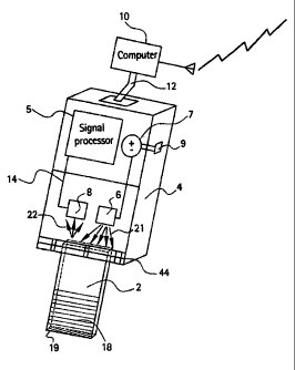
Fig. 1 is a perspective view of a handheld sensor system according to an
embodiment
of the present invention;
Fig. 2 is a frontal view of a multisectional disposable optical element
according to an
alternative embodiment of the present invention;
Fig. 3 is a perspective view of a disposable test element according to an
embodiment
of the present invention;
Fig. 4 is a perspective view of a handheld sensor system according to an
embodiment
of the present invention using a multisectional test element;
Fig. 5 is an example of a dual wavelength response from a single analyte;
Fig. 6 is an example of a series of absorption levels showing a change in
spectral
response from exposure of different concentrations of ink to light;
Fig. 7 is a perspective view of another measurement configuration according to
an
example presented by the present invention;
Fig. 8 is an example of a baseline spectrum and sample spectrum obtained with
a
polycarbonate reflection element;
Fig. 9 is an example of a sample spectra for 0.5 ppm NaOCI before reference
corrections and whereby the optical element position was tightly controlled;
Fig. 10 is an example of a sample spectra for 0.5 ppm NaOCI after reference
correction and whereby optical element position was tightly controlled;
7
CA 02552752 2006-07-06
WO 2005/073696 PCT/US2005/000092
Fig.. l l is an example of a calibration curve for, reference corrected
absorbance listed
in Table l;
Fig. 12 is an example of a sample spectra for 0.5 ppm NaOCl before reference
correction and whereby optical element position was not tightly controlled;
Fig. 13 is an example of a sample spectrum for 0.5 fpm NaOCI after reference
correction and whereby optical element position was not tightly controlled;
Fig. 14 is a schematic description of the measurement configuration used for
Example
1;
Fig. 15 is a schematic description of the handheld sensor system for Example
5;
Fig. 16 is a perspective view of the handheld sensor for Example 5; and
Fig. 17 is a calibration curve obtained with the handheld sensor described in
Example
5.
DETAILED DESCRIPTION OF THE INVENTION
The present invention pertains to a method and apparatus for measuring the
concentrations of chemical substances by utilizing the reactive properties of
certain
chemical substances; for example, the property of the substance to react with
another
chemical, e.g., a select analyte, causing a chemical change in the first
reagent, and
resulting in a change in the light absorbing properties of the original
chemical-
containing material. In operation, the present invention measures the test
element
response to specific analytes through a change in light absorbance,
luminescence,
light scattering, or other light-based response. The analytes described in
this invention
are chemical species, but this invention can also be envisioned to include
biological
systems where bioanalyte interactions stimulate similar test element response.
As an
example, such biological systems could be immobilized enzymes that stimulate
light
response proportional to an analytes concentration, for example, luciferase
response to
adenosine triphosphatase (ATP).
8
CA 02552752 2006-07-06
WO 2005/073696 PCT/US2005/000092
With reference now to the drawings, Fig. 1 shows a basic sensor system
comprising a
disposable test element 2, which is approximately the size of a glass
microscope slide,
detachably mounted onto adapter 4. The test element 2 is made of any
reasonably
transparent substance such as glass or organic polyrieric material that has a
refractive
index (n~) that is usually greater than unity. A portion of the test element
is coated on
one or both sides with a thin, transparent polymer film containing reagents
that are
needed to react with analytes i~ order to produce a color product. The reagent
film
can be immobilized onto the test element by dip coating or spin coating the
test
element, or by other means known in the art. In addition, to coating a portion
of the
test element, it is understood that the entire test element may be coated as
well. In
combination with the above mentioned reagent substance, the reactive film
coating
also includes a reference dye which serves to provide an internal light
absorbance
standard, or internal reference, whereby the refractive ~ index of the reagent-
dye film
mixture (n2) can be less or more than n~. The reference dye is mixed together
with the
film coating to provide a reagent film complex having a constant internal
light
absorbance standard. In other words, the reference dye component of the
reagent film
complex provides a first light absorbance response, and the reagent itself
'provides a
second light absorbance response, allowing the reagent elm complex to provide
a
dual light absorbance response (i.e. dual light response) to incident light
energy.
However, unlike the reagent itself, the reference dye does not react with the
analyte.
Accordingly, the dye's spectral profile would remain constant from one test
element
to another, and before and after the test element is exposed to the samples if
the
optical and mechanical properties of the test element have not changed.
Moreover,
since the reference dye and reagent have different light absorbance spectrum,
the
reference dye's spectral profile does not appreciably overlap with the target
detection
wavelength, or range of wavelengths, used to measure the test element response
to the
reaction between reagents and the analyte. By providing such a non-overlapping
benchmark response differential between the reference dye and the reagent, the
reagent film complex provides an internal light absorption standard or
internal
reference, thus providing an internal dual light response which eliminates the
need for
external calibration and device calibration before each new set of analyses.
As
discussed in more detail below, it is understood that the internal reference
also
9
CA 02552752 2006-07-06
WO 2005/073696 PCT/US2005/000092
minimizes response variation from device . to device, providing substantial
manufacturing and maintenance cost advantage with minimal impact on the
accuracy
of test. results. As a consequence, the characteristics and features of the
present
system are well suited for cost effective production, assembly, and
miniaturization.
The internal reference cited above is a colorimetric dye, but this is just one
of many
possible embodiments. Any standard that does not react with the
analyte'detection
chemistry and that has a spectral response outside the detection spectra can
act as an
internal standard. This material can be an inorganic complex, a pigment, dye,
or
micro- or nanoparticle that produces the desired spectral response and can be
used to
correct the errors due to film variations.
Referring again to Fig. l, the mounting adapter 4 comprises at least one light
source 6,
which can be any means that is capable of emitting light energy 21, such as
LED,
laser diode, or miniature light bulb. The adapter 4 further comprises at least
one
photodetector 8, which can be any means that is capable of detecting light
energy 22
and converting said energy to electrical output signals that are indicative of
the test
elements response to the target analyte or analytes. These electrical output
signals are
transmitted to signal converter 5 via circuit wire 14. It is understood that
many
commercially available photodetectors could be used to achieve the desired
performance, such as photodiode, micromachined photo multiplier tube, or
photocell,
and are well known in .the art.
The adapter 4 also includes fixturing means 44 serving to align the test
element 2 and
locate it in a reasonably reproducible position with respect to the light
source 6 and
photodetector 8. As discussed in more detail below, the present invention does
not
require fixturing means 44 to provide strict positioning and control of the
test element.
Rather, it has been discovered that a modest or reasonable control of the test
element
2 with respect to the light source and photodetector is effective to achieve
accurate
and reproducible absorbance results, thereby offering cost advantage in the
manufacturing, maintenance, and assembly requirements.
In operation, with power switch 9 activated, the light source 6 produces an
uncollimated and unfocused light beam. As best shown in Fig. 3, the
uncollimated
CA 02552752 2006-07-06
WO 2005/073696 PCT/US2005/000092
and unfocused light beam impinges the test element at different angles; that
is, at
angles less than and greater than the critical angle of the test element. As
discussed in
more detail below, a portion of this incident light energy reacts with the
reagent film
complex immobilized oii the test element. Once such incident light energy
passes
thrOllgh the reagent film complex, the photodetector is capable of detecting a
pair of
light response spectra; that is, the photodetector detects a first light
response from the
internal reference dye alone, ayd a second light response from the reagent
film itself,
thereby allowing the device to detect a dual light response from the incident
light-test
element interaction. In this way, any changes in the test element light
response
spectra can be detected and measured without the need for external calibration
before
each new set of analysis. Furthemnore, it will be shown that due to the
uncollimated
and unfocused nature of the incident light beam, strict control and
positioning of the
test element by fixturing means 44 is not required to provide relatively
accurate test
results. Rather, fixturing means 44 need only provide a modest or reasonable
positional control for the test element 2, thereby providing cost savings in
.the
manufacturing process.
The adapter 4 further comprises battery 7 to power the sensor system; although
skilled
artisans will appreciate that many alternative means to power the sensor
system may
be used as well. In addition, suitable electronic means are provided which
allow the
signal converter 5 to communicate with signal processing unit 10 so that the
electl'ical
output signals generated by the photodetector 8 can be processed and stored
electronically. It is understood that many well-known configurations can be
utilized
in a manner known in the art to achieve the same performance . as the above
embodiment, including an embodiment capable of communicating via interface 12
with an external processing unit 10, for example a handheld computer, PDA, or
other
wireless transmission device. Moreover, it is understood that an embodiment
comprising a built-in processing unit (not shown) could be used as well.
By way of example, and not by way of limitation, the light source 6 is
positioned
proximate an edge of the detachable test element 2 so that incident light
waves 21
emitted from the light source impinge an edge 23 of the test element, where
the
uncollimated and unfocused light beam from the light source impinges the test
CA 02552752 2006-07-06
WO 2005/073696 PCT/US2005/000092
element at a plurality of different angles as best shown in Fig. 1. It is well
known that
a critical angle of the test element may be calculated from the refractive
index of the
substrate (n2) and that of air (n~) through eguation O~ = siri' (n2 / n~),
where O~ is the
critical angle: Referring now to Fig. 3, a divergent light beam 21 is directed
toward
the edge of the test element at approximately 45°. Since the light beam
21 is
unfocused and uncollimated, some of the incident photons 21 impinge the test
element 2 at angles' greater than the critical angle, while other incident
photons
impinge the test element at angles less than the critical angle. In the event
that the
incident angle of the photons 21 is greater than the critical angel O~, tie
light beam
will be totally reflected at the film-air interface. This phenomenon is called
total
reflection. On the other hand, if the incident angle of the light beam 21 is
less than O~,
the incident light beam will be partially reflected at the film-air interface.
This
phenomenon is called partial reflection.
In the case of total reflection, although a portion of the light beam 21 will
be totally
reflected at. the film-air interface of the test element, a portion of the
reflected light
energy can penetrate into the film and reenter the substrate as if it has
traveled a short
distance parallel to the interface. This energy is called an evanescent field
or
evanescent wave 20E as shown in Fig. 3. Since a reactive film coating 18 has
been .
immobilized onto the surface of the test element, a portion of the evanescent
wave
20E will be absorbed (attenuated) by the film coating 18 at the substrate-film
interface. This phenomenon is called attenuated total reflection (ATR). In the
case of
partial reflection, the partially reflected photons of the incident light beam
21 are
similarly capable of forming an evanescent wave 20E and becoming absorbed by
the
film coating, while the remaining un-reflected photons may be lost into the
surrounding environment. This phenomenon is called Attenuated Partial
Reflection
(APR). To increase the effectiveness of APR, a reflective coating 19 can be
immobilized onto an end of the test element, whereby un-reflected incident
light. 20
that has penetrated into the body of the test element may reflect against the
reflective
coating 19 and scatter back through the test element. Consequently, a portion
of these
internally reflected photons 20 are provided with another opportunity, or
"second
chance", to form an evanescent wave and react with the film coating 18 at the
surface
12
CA 02552752 2006-07-06
WO 2005/073696 PCT/US2005/000092
of .the test element. Accordingly, since the present invention includes
components
from both ATR and APR, it is possible to improve the efficiency of the
incident light
beam 21 without the need for costly optical devices or coupling requirements,
thereby
providing advantage over well-known ATR systems.
Referring again to Fig. 3, as the evanescent light wave 20E propagates along
the
surface of the test element, a portion of these evanescent photons are able to
interact
with molecules contained in the reactive Elm 18. This interaction causes a
portion of
the evanescent photons to become absorbed by the molecular structure of the
reactive
Elm. Accordingly, the photons 22 that were lucky enough to avoid becoming
absorbed by the reactive film 18, and were not otherwise lost to the
environment, will
be transmitted from the test element where they may be ultimately detected by
the
photo detector 8. Since the number of photons 22 that are ultimately
transmitted from
the test element depends upon the absorbance level of the incident light beam
21, it is
possible to utilize electrical signals generated by the photo detector to
indicate the
absorption percentage of the reactive film. Once the relative intensity of the
ultimate
light response is compared with known reference data, it is possible to detect
and
determine the analyte concentration of the sample substance.
As described above, when power switch 9 is activated and light beam 20 is
projected
onto the test element, the photo detector receives a dual light response 22
from the test
element. Such response curve is illustratively shown in Fig. 5. Here, line 100
represents the light response of the film coating before the test element is
exposed to
the sample analyte, and line 200 represents the dual light response of the
film coating
after the test element is exposed to the sample analyte. Ao represents the
absorption
level of the film coating alone at wavelength ~,2. The first peak at A~
represents .the
absorption level of the internal reference dye at wavelength ~,~ before
exposure, and
AZ represents the absorption level of the internal reference after exposure.
Values of
A~ and AZ would be the same, if the optical and mechanical properties of the
test
element have not changed during the exposure. The peak at A3 represents the
absorption level of the Elm coating at wavelength ~,2 after the test element
is exposed
to the sample analyte. If it is known that the sample substance absorbs light
in
13
CA 02552752 2006-07-06
WO 2005/073696 PCT/US2005/000092
proportion to the concentration of the substance present in the sample, it can
be shown
that the difference between the absorption levels A3 and Ao is proportional to
the
analyte concentration of the sample substance. By taking into account the
absorbance
levels (A~ and AZ) of the internal reference centered at ~,t, it is possible
to calibrate the
absorbance levels of the reagent film coating according to the general
formula:
( 1 ~ Acorrected - A3 - AO ~' (A 1 - A2),
where Aeo~.~.eeted represents the normalized absorbance level of the reagent
film coating.
It is understood that many alternative procedures, such as comparing peak-to-
peak
ratios or areas under the curve could also be used to normalize the response
curve.
In order to calculate absorbance, blank signal outputs at ~,~ and ~,2 of the
test element
before a reagent film is coated have to be known. The signal sensor response
can be
obtained by measuring the photodiode signal when a test element without the
polymer
film is loaded. The blank response can be stored in the processor. It will
become
clear in the following section that the anal result Aeorreetea is independent
of the blank
response. Knowing the blank response allows the absorption level of the test
element
before exposure to be expressed as absorbance unit rather than volts or
amperes
measured by the photodiode.
In a preferred mode of operation, the polymer coated test element 2 is
detachably
mounted to the adapter 4 by ~xturing means 44. As described above, fixturing
means
44 aligns and locates the test element in a reasonably reproducible position
with
respect to the light source and photodetector. Strict control of the incident
light angle
and test element with respect to the light source and photodetector is not
required. In
order to compensate for variable lighting conditions, once at the sample test
site the
operator activates the light source to record the corresponding reflection
intensities
from the coated test element. The light response spectra measured during this
step are
referred to as baseline intensities.
14
CA 02552752 2006-07-06
WO 2005/073696 PCT/US2005/000092
After the baseline intensity response is established, the operator proceeds to
expose
the coated test element to the chemical or biological sample substance for a
given
period . of time, for example 1-3 minutes, depending on the diffusivity of the
film
coating. Next, the operator removes the test element from the sample, and
excess
liquid sample is allowed to run down or off the test element. This step may
take 0-5
minutes. After this period, the operator again activates the light sources to
record the
corresponding reflection intensities from the sample exposed test element. The
light
responses measured during this step are referred to as sample intensities.
Continuing the above analysis, the accumulated data representing the blank,
baseline,
sample and internal reference response intensities are processed and combined
with
known chemical reference data corresponding to the expected spectral response
of a
particular analyte under inspection. As shown and discussed in more detail in
Examples 1-5 below, by comparing the intensity of the light response after the
test
element is exposed to the analyte with the intensity of the light response
before the
test element is exposed to the analyte, it is possible to measure the analyte
concentration of the sample substance. ,
The system described above shows photometric measurement carried out with
conventional optical devices. As a result of the multiangle scatter-induced
absorbance
measurement technique utilized by the present invention, it is possible to
achieve
accurate, reproducible absorbance measurements for elms with higher
sensitivity than
is possible with traditional transmission measurement techniques for these
films. This
is because traditional transmission absorbance measurement techniques can be
characterized as "one pass"; that is, incident photons in traditional
transmission
techniques get "one pass" through the substance under inspection, allowing the
photons a single opportunity to react with the test element as they propagate
through
the substrate with minimal refraction and scattering. In contrast, as best
shown in Fig.
3, the present invention utilizes a multiangle scattering approach whereby
incident
photons 21 scatter inside the test element and reflect against the reflective
coating 19,
thereby allowing a portion of the incident photons to have "multiple passes"
through
the test element. This multiangle scattering approach increases the
lilcelihood that
evanescent photons 20E will ultimately react with the film coating on the
surface of
CA 02552752 2006-07-06
WO 2005/073696 PCT/US2005/000092
the substrate. As such, if an incident photon fails to evanesce the surface of
the
substrate on its initial pass, there is a high probability that the same
photon will scatter
inside the test element and ultimately reflect back towards the surface of the
substrate,
thus providing such photon with another opportunity to evanesce the surface of
the
substrate and ultimately become absorbed by the film coating. Accordingly, it
is
possible for a given amount of light energy to achieve a larger proportion of
absorption events compared, to traditional transmittance techniques, thereby
increasing the relative absorbance percentage of the incident light, and
improving the
ultimate sensitivity of the sensing device. , ,
It is important to note that many configurations of the same major components
can
achieve the same performance as the above embodiment. For example, another
embodiment of the present invention is illustratively shown in Fig. 2. Here,
there is
shown a multisectional optical test element 2A comprising separation regions 3
and
sensing regions 5. The separation regions act, as barriers between the sensing
regions
by absorbing scattered light that may become reflected at the several sensing
regions,
thereby reducing interactive noise between the sensing regions. Each sensing
region
utilizes an independent reactive film coating comprising its ~ own internal
chemistry.
Each of these reactive film coatings and their accompanying chemistries are
effective
to provide an independent dual light (spectral) response from a particular
analyte of
interest in the sample solution. Accordingly, a plurality of analytes cad be
simultaneously tested on a single test element. Moreover, it has been
discovered that
the separation regions 3 can be perforated for improved separation, thereby
increasing
the effectiveness of the test element.
To facilitate operation of the multisectional test element, it is contemplated
that, an
independent light source and photodetector pair can be provided for each of
the
independent sensing regions, whereby .each source and detector pair is capable
of
generating an appropriate dual light response from each of the several sensing
regions. Alternatively; a single light source and photodetector may be
configured to
generate and detect a suitable dual light (spectral) response from each of the
independent sensing regions. In this case, the independent electrical signal
generated
by each of the several sensing regions can be combined and multiplexed in a
manner
l6
CA 02552752 2006-07-06
WO 2005/073696 PCT/US2005/000092
known in the art by processing unit 10 to detect and quantify a plurality of
analytes
with a single disposable test element.
Fig. 4 describes an apparatus to facilitate the multisectional test element.
This
apparatus has the same basic components as for the. system shown in Fig. 1.
The
exemplary embodiment of Fig. 4 comprises several pairs of light sources 6 and
photodetectors 8 which can be mounted on the two 'sides of adapter 4A. The
multisectional test element 2A is mounted onto the fixturing means 44. Here,
the
fixturing means 44 is attached to a mobile carriage of miniature motion slide
66. The
motion slide allows the test element to be retrieved inside the adapter and
serves to
align the test element with the light source/photodetector pairs for
absorbance
measurements. Suitable electronic means 77 are provided for controlling the
device
so that electrical output signals generated by the photodetectors can be
processed and
stored electronically.
The present invention also contemplates the utilization of additional sensors
that
could be used to provide information about the ambient atmospheric conditions
such
as temperature (for example, using a thermister), relative humidity (for
example,
using a capacitance humidity sensor), and atmospheric pressure (for example,
using a
MEMS pressure sensor) and are well known in the art.
In another embodiment, the chemical sensor system contemplates a dynamic
pattern
recognition system for improving the functionality and quantitative ability of
the
sensor array. The functionality of the sensor array is improved by having
means of
indicating the end of the required environmental exposure of the sensor. For
example,
the sensor is immersed into a water sample until an alarm (for example, a
sound beep)
indicates that the sensor is ready to be withdrawn and is ready to provide
quantitative
information. The operative principle of such system is based on the use of the
dynamic signal analysis of the sensor response. In particular, the sensor in
the present
invention can collect dynamic data during a specified time period by tracking
the rate
of change of the response of the non-reversible sensor chemistries as the
sample
reacts with the sensor in order to quantify the concentration level. Thus, our
sensor is
more information-rich compared to the sensors that are simply exposed to a
sample
17
CA 02552752 2006-07-06
WO 2005/073696 PCT/US2005/000092
and further withdrawn when the signal measured after the withdrawal. This
collected
dynamic data can be analyzed for known parameters such as initial,
intermediate, and
final slope of signal during exposure. These dynamic parameters can be used to
indicate when a steady-state response is reached. If the steady state cannot
be reached
in a reasonable period, the dynamic parameters can be used to quantify the
analyte
concentration. Additionally, the slope of the chemical sensor response can be
more
sensitive than the equilibrium ,end point, and result in increased sensitivity
for the
sensor system described here.
In yet another embodiment, the sensor has another alarm that indicates the
time of
analysis completion after the sensor is withdrawn from the sample. This data
is
provided by different signal recovery rates from different sensor regions,
which are
dependent on the sensor chemistry, reversibility, and ambient atmospheric
conditions.
As skilled artisans will appreciate, many suitable electronic, integrated
circuit and/or
microprocessor means may be configured to provide 'the above-mentioned sensor
and
timer alarm features to obtain the collection of dynamic sensor response data
of the
contemplated embodiments described above. In one embodiment shown in Fig. 15,
a
Visual BasicOO computer program was developed to provide the timer and alarm
features and to control arid read the sensor system.
It is well lcnown that reversible chemical sensors often suffer from poor
response
selectivity, and this is primarily due to interference or noise from non-
specific signal
changes. Accordingly, the selectivity of chemical recognition can be improved
with
non-reversible, disposable sensors. Non-reversible sensor chemistry often
provides
stronger and more selective interactions between the reactant and the chemical
species
of interest, and this is generally viewed as one of the advantages created by
non-
reversible sensor chemistry. However, if it is advantageous to improve the
sensor's
dynamic range or reduce chemical interferences, it may be desirable to analyze
a
single analyte using several sensor regions containing different reagents, or
complimentary sensor elements that in combination enhance the overall system
response. Despite the known disadvantage associated with reversible reagents,
one
can include a reversible reagent in a mufti-reagent detection scheme to
improve the
overall sensor response. This combination of a reversible and non-reversible
platform
CA 02552752 2006-07-06
WO 2005/073696 PCT/US2005/000092
can create a system with enhanced capabilities. Standard pH indicators are one
example of chemicals commonly used in reversible sensors while the chlorine
reagent
described in the following examples is an example of nonreversible chemistry.
As a
non-limiting example, combining a reversible pH sensor with a non-reversible
chlorine sensor makes it possible to further define other chlorine-containing
species
present in the sample. ,
With reference now to the following examples, it has been discovered that a
modest
or reasonable control in the coupling and positioning requirements of the test
element
and optic components, as opposed to a strict or critical control of such
coupling and
positioning requirements, is effective to achieve accurate and reproducible
absorbance
results if an internal reference absorbance standard is used according to the
following
equation:
Acorrected - Asample ' Abaseline + ~Abaseline-at preference - Abaseline at
~sample~~
However, it is recognized that utilizing a single internal absorbance standard
does not
remove all the errors caused by variation in film or substrate quality and the
alignment
of the test element with respect to the incident beam. This is because each
error
source has a different effect on the absorption bands at different
wavelengths. 'For
example, a change in absorbance caused by a change in the angle of incidence
is a
function of wavelength, not chemistry, since the optical path length is
dependent on
wavelength. Thus, it is recognized in the present invention that using a
referencing
system with more than one internal standard can increase accuracy or by using
the
spectral profile of a single standard absorption band if whole spectra are
measured.
But it is important to note that a reasonably high level of reproducible
measurement
has been achieved by utilizing a single internal absorption standard in
combination
with a modest or reasonable mechanical control coupling between the disposable
test
strip and adaptor, as demonstrated by the following examples.
19
CA 02552752 2006-07-06
WO 2005/073696 PCT/US2005/000092
Example 1
Four edges of a Fisher brand, clear glass slide (dimensions 3" x 1" x 0.41 ",
Fisher
catalog number 12-549) were painted with a white ,paint pen (Uni~Paint PX-20)
as
shown in Fig. 14. An area near one end was also painted with the white paint
pen.
The arrangement of LED and photocell is shown in Fig. 14. The light source was
a 5
mm, 3000 mcd red LED, with peak emission wavelength at 660 nm and a viewing
angle 12° available from ~RadioShackOO. Absorbance levels of different
concentrations of blue lines made with a permanent, fine point Sharpie~ marker
are
shown in Fig. 6. Here, during the initial time interval 0-22 seconds, light
was
projected onto a blank (no blue marking) glass slide. As expected, the
corresponding
absorbance level shown at line 50 is approximately zero. After approximately
22
seconds, a single blue line was made on the glass , slide, and the
corresponding
absorbance level increased to line 51 as shown. After approximately 34
seconds, a
second blue line was made on top of the first blue lint to increase the
concentration of
blue marking on the glass slide.. As expected, the corresponding absorbance
level
increased to line 52. Similarly, after approximately 45 seconds, a third blue
line was
added to further increase the concentration of blue marking on the glass
slide. Again
as expected, the corresponding absorbance level increased to line 53. It is
well known
that the absorbance for this measurement is defined as:
~S
(3) A = log[(photocell output for a clear glass slide - output at
dark)/(output for blue lines - output at dark)];
where output at dark is the steady state response of the detector when the
light source
is turned off.
This example demonstrates that photometric measurements may be conducted in a
very simple manner. However, many designs can be built from this simple setup.
For
example, interference filter films can be coated in the areas facing the
photodetector
CA 02552752 2006-07-06
WO 2005/073696 PCT/US2005/000092
or mixed into the reflective paint. so that absorbance for a given absorption
band can
be measured. Fig. 2 illustrates one of these designs.
Example 2
In this second example, a 3.7" x 0.49" x 0.21" polycarbonate reflection
element was
made. An end 'of the polycarbonate element was beveled to an angle equal to
approximately 51 °. fihe test element configuration for absorbance
measurement used
in this example is shown in Fig. 7. Here, an Ocean Optics P400-2 six optical
fiber
bundle was used to provide the incident light from an Ocean Optics tungsten-
halogen
lamp. An 8400-7 Ocean Optics reflection probe was used to collect the
reflected
light to an Ocean Optics USB2000 spectrometer. Before a poly (2-hydroxylethyl
methacrylate) (PHEMA) film containing tetramethylbenzidine (TMB) was dip
coated
on one side of the polycarbonate element, a blank spectrum with zero
absorbance for
all wavelengths was established. After the TMB film was coated, the
polycarbonate
element was put back to the configuration as shown in Fig. 7. Here, a baseline
spectrum was first recorded. Next, a 0.06 ml 0.1 ppm sodium hyperchlorite
solution
was carefully spread to cover a 3 mm x 12 mm area over the TMB film. ~ After
staying
on the TMB film for 1 minute, NaOCI solution was carefully removed with aid of
a
paper towel. The sample spectrum was measured 4 minutes after the NaOCI
solution
was spotted on the TMB .film. Both the sample spectra 110 and baseline spectra
120
are shown in Fig. 8.
Example 3
The same Ocean Optics spectrometer system from Example 2 was used in this
example. A microscope slide holder tightly controlled the positioning of the
glass
slide. The incident optical fiber probe was directed to one side of the glass
slide at
roughly 45° angle with respect to the glass slide plane. About half of
the incident
light illuminated the white paper underneath the glass slide and the other
half
illuminated an edge of the glass slide. The detection probe was also angled at
about
45° and the distance from the probe to the slide was adjusted so that
the amount of
light does not saturate the spectrometer.
21
CA 02552752 2006-07-06
WO 2005/073696 PCT/US2005/000092
A PHEMA film containing a small amount of red dye was recovered from a
permanent red SharpieQ marker. A solution of red dye was spin coated on glass
slides as in Example 1 with a spirmer modified from a magnetic stirrer, which
does
not have speed control or readout. The spinner acceleration, the final spin
speed, and
spinning duration were not controlled. The red dye is used as the internal
absorbance
standard. It has an absorption band centered at a,",aX = 535 mn, which does
not overlap
the absorption band of the TM$ reaction response to chlorine (blue reaction
product,
~,,",aX = 670 nm).
Before the slides were immersed into NaOCl solution, a baseline spectrum for
the
TMB was measured. After a 90-second immersion in the NaOCI solution, the glass
slide was removed and held at a vertical position for 2 minutes so that
solution on the
glass slide surfaces could run down. Here, the sample spectrum was recorded
150
seconds after the glass slide was removed from the NaOCI solution.
A total of 11 slides were used according to the above procedure to measure the
absorbance values at three different concentration levels of NaOCI solution.
Slides 1-
4 were independently immersed into an 0.10-ppm solution, slides ~ 5-7 were
independently immersed into an 0.25-ppm solution, and slides 8-11 were
independently immersed into an 0.50-ppm solution. The absorbance values at ~,
= 650
nm before and after reference correction are listed in Table 1 below. It is
important to
~S
note that the standard deviation for each concentration level is significantly
reduced
after reference correction was performed according to equation 1.
Table 1. Absorbance values before and after reference correction.
Before After
Correction Correction
NaOCI/ppm Slide#AbsorbancAverage +/- AbsorbancAverage +/-
a standard a standard
deviation deviation
22
CA 02552752 2006-07-06
WO 2005/073696 PCT/US2005/000092
0.1 ppm 1 0.047 0.041 ~ 0.0150.057 0.053 ~ 0.004
2 0.057 0.049
3 0.021 0.051
4 . 0.038 0.056
0.25 ppm 5 0.168 0.151 ~ 0.0150.095 0.100 ~ 0.008
6 0.146 0.096 ,
7 0.140 0.109
0.05 ppm 8 0.206 0.188 ~ 0.0180.181 0.179 ~ 0.003
9 0.192 0.181
10 0.163 , 0.175
The four spectra from .slides 8-I1 and their corresponding baseline spectra
are
presented in Fig. 9.
All 11 spectra after reference correction according to equation 1 are shown in
Fig. 10.
Fig. 10 graphically demonstrates that normalizing the results according to the
internal
absorbance standard, as described by equation 1, reduces error and confirms
the
results listed in Table 1.
Fig. 11 shows a calibration curve confirming the linear relationship between
absorbance levels and concentration levels as known in the art.
Several conclusions can be drawn from the results obtained in this example:
23
CA 02552752 2006-07-06
WO 2005/073696 PCT/US2005/000092
1. Appropriate positional ~ control alone does not ensure the accuracy
needed for low absorbance measurements.
2. Using an internal absorbance standard to correct spectra according to
equation 1 reduces errors caused by variations in experimental parameters such
as
glass slide dimension, film quality, and incident beam angle.
3. Multiangle scatter-induced absorbance is more sensitive than
transmission absorbance. In comparison with the transmission absorbance value
at ~,
= 535 nm (0.014) a 10-fold increase in absorbance is achieved with the
multiangle
scatter-induced configuration of the present invention. It is important to
note that
even greater increases can be expected with longer wavelengths.
Example 4
The films used in this example contained a slightly lower concentration of the
internal
reference dye compared to the films used in Example 3. These films were
prepared
by the same procedure used in Example 3, but were produced in a different
batch.
Similarly, the experimental setup was the same as used for Example 3, except
the
slide position was only loosely controlled by aligning the slide with respect
to two (2)
perpendicular lines drawn with a Sharpie~ marker.
The spectra response before and after reference correction together with
baseline
spectra response are shown in Figs. 12 and 13 respectively. It is evident that
measurements derived without maintaining appropriate control of the glass
slide
position results in a larger margin of error, despite the reference correction
from the
internal absorbance standard. Nevertheless, it is important to note that the
absorbance
values at 650 nm 0.177, 0.185, and 0.209 agree well with the average values of
'0.179
~ 0.003 obtained from Example 3, even though the slide position was not
tightly
controlled and the films were prepared in a different batch and from a
different
polymer solution. This agreement is significant, especially in view of one
objective
of the present invention; that is, to provide for the quantitative
determination of
analyte concentrations by way of a disposable test element, without an
additional
calibration step.
24
CA 02552752 2006-07-06
WO 2005/073696 PCT/US2005/000092
Example S
Sensor construction
A schematic diagram of an exemplary handheld sensor system used for Example S
is
shown in Fig. 1S. Here, the basic sensing unit 1S0 is shown connected to
digital bus
switch 1 S2 (Texas Instruments, SN74CBTLV) and computer 1 S 1 (Dell Axiom
Pocket
PC equipped with Dataq CF2, C-Cubed Limited data acquisition card). The
digital
bus switch 1S2 was used to allow the computer to turn ON and OFF the LED 6
while
providing DC. power to the photodiode 8, and allowing the output from the
photodiode to be read. A Visual BasicOO computer program was developed to
control
and read the sensor system.
A perspective diagram of an exemplary sensing unit 1S0 used for Example S is
shown
in Fig. 16. Here, the sensing unit 1 SO can be described as comprising a
combination of
three sub-assemblies: Part A; Part B; and Part C.
Part A comprises elements 160, 161, and 162. Part B comprises elements 6, 8,
163,
and 164. Part C comprises elements 18, 19, and 167.
In constructing Part A, the threaded part of a '/2-inch instant tube-to-pipe
adapter 161
was removed and a '/4-inch compression fitting nut 162 was glued onto the face
of the
modified adapter 161. A 4-inch long, '/z OD stainless steel tube 160 is
inserted onto
the rubber O-ringlcompression fitting 161 C of the modified adapter to provide
a light
tight compartment.
In constructing Part B, the male part of a'/a inch tube-to-pipe compression
fitting I63
was removed, and a thin polycarbonate sheet 164, which was painted black on
one
side, was fixed to the modified fitting with epoxy glue so that the opening of
the
modified fitting is divided as best shown in Fig. 16. A S mm bicolor LED 6 (LC
LED
NSOOTGR4D) was glued onto the polycarbonate sheet. The focal path of the LED 6
is approximately parallel to the vertical center of the fitting 163. A
photodiode 8
(Toas TSR2S7) was attached to the other side of the polycarbonate sheet so
that the
collection lens of the photodiode is offset from the axis of the fitting with
an angle of
2S
CA 02552752 2006-07-06
WO 2005/073696 PCT/US2005/000092
about 45° as shown in Fig. 16. After the above construction, the LED
and photodiode
were sealed inside a 1-inch diameter PVC tube (not shown in Fig. 16).
In constructing Part C, an acrylic rod (0.25 inch diameter and 3.20 inch long)
167 'was
coated with PHEMA film containing chlorine sensitive reagents 18 as used in
Example 3. The end section of the rod was painted with reflective white paint
19.
Measurement procedure
The measurement procedure used for Example 5 comprised the following steps:
1. (a) Load the acrylic rod 167 (Part C) into the compression fitting assembly
(Parts A and B) and put the stainless steel tube 160 into the instant tube-to-
pipe adapter 161; (b) Click the button on the Pocket PC screen; (c) The Visual
BasicO computer program turns on the green (525 nm) and red lights (630
nm) sequentially, and takes respective readings (G° and R°) from
the
photodiode while the green and red lights are turned ON.
2. (a) Remove the stainless steel tube 160 from the adapter 161 and dip the
rod
167 into a sample solution for 60 seconds; (b) Pull the rod from the solution
and remove remaining solution with a suitable wipe; (c) Let the rod dry for
two minutes in air.
3. (a) Put the stainless steel tube 160 back onto the adapter 161; (b). Click
the
appropriate button on the Pocket PC screen to read respective outputs G and R
from the photodiode. Note that both the green and red light are turned ON
sequentially.
4. Calculate absorbance with equation 2.
A = log(R°/R) - log(G°/G) (2)
26
CA 02552752 2006-07-06
WO 2005/073696 PCT/US2005/000092
Note that equation 2 is mathematically equivalent to equation 1. The results
from
these measurements are listed in Table 2 and plotted as a calibration curve in
Fig. 17.
Table 2. Results for Example 5
NaOCI/ppm Ro/V Go/V R/V G/V Absorbance
0.00 1.873 1.762 1.852 1.780 0.009
0.00 1.937 1.829 1.895 1.835 0.011
0.00 2.055 1.941 2.002 1.944 0.012
0.096 1.960 1.867 1.891 1.864 0.015
0.096 2.079 1.965 1.939 1.928 0.022
0.096 1.946 1.847 1.808 1.802 0.021
0.20 1.998 1.843 1.835 1.809 0.029
0.20 1.916 1.835 1.816 1.827 0.022
0.20 1.936 1.846 1.805 1.824 0.025
0.49 1.964 1.847 1.732 1.805 0.045
0.49 1.995 1..875 1.756 1.831 0.045
0.49 1.855 1.780 1.646 1.752 0.045
0.97 1.926 1.806 1.556 1.743 0.077
0.97 1.979 1.871 1.615 1.808 0.074
0.97 1.936 1.852 1.525 1.772 0.084
27
CA 02552752 2006-07-06
WO 2005/073696 PCT/US2005/000092
1.99 1.901 1.805 1.360 1.695 0.118
1.99 1.957 1.868 1.340 1.754 0.137
1.99 1.899 1.806 * ~ 0.136
* data were missed
While the specification above has been drafted to include the best mode, of
practicing
the invention as required by the patent statutes, the invention is not to be
limited to
that best mode or to other specific embodiments set forth in the
specification. The
breadth of the invention is to be measured only by the literal and equivalent
constructions applied to the appended claims.
28