Note: Descriptions are shown in the official language in which they were submitted.
CA 02552958 2006-07-10
WO 2005/057582 PCT/AU2004/001735
-1-
A MEMORY DEVICE, AN INFORMATION STORAGE PROCESS, A PROCESS,
AND A STRUCTURED MATERIAL
FIELD OF THE INVENTION
The present invention relates to a memory device, an information storage
process, a
process, and a structured material.
BACKGROUND
The rapid progress in microelectronics is often represented by Moore's Law,
which
predicts that the number of transistors per integrated circuit will continue
to double every
couple of years. This doubling requires the physical size of each transistor
to decrease
with each successive generation of integrated circuits. However, the
difficulty of
achieving this shrinkage has increased dramatically, to the point where it may
not be
economically feasible to continue to follow Moore's Law due to exponential
increases in
complexity and the time required to develop new generations of integrated
circuits. On the
other hand, the enormous demand for memory chips, as opposed to
microprocessors, may
justify such high development costs for memory devices. Yet the challenges of
developing
ever smaller memory devices remains considerable, particularly as the
characteristic
dimensions of such devices enter the nanometer scale.
Existing random access memory (e.g., SRAM, DRAM) devices store information in
an
array of memory cells, with each cell storing a single bit of binary data. In
a typical
memory device, the bit of data stored in a particular cell can be accessed by
applying an
appropriate potential to the wordline connection to the array row containing
the cell and
measuring the resulting potential of a bitline connection to the cell. One of
the, difficulties
of existing memory devices is that the ability to reduce the physical
dimensions of each
cell is limited, placing an upper limit on the density of information storage.
For example,
in the case of transistor-based memory devices, although the gate length of
each transistor
CA 02552958 2006-07-10
WO 2005/057582 PCT/AU2004/001735
-2-
is extremely small (typically around 100 nm in current technology), the total
surface area
or footprint of each cell is at least an order of magnitude larger. There is
thus a need for a
memory device with a simpler structure that would allow a higher density of
cells to be
produced.
It is desired, therefore, to provide a memory device, an information storage
process, a
process, and a structured material that alleviate one or more difficulties of
the prior art, or
at least provide a useful alternative.
SUMMARY OF THE INVENTION
In accordance with the present invention, there is provided an information
storage process,
including applying pressure to and removing pressure from one or more regions
of a
substance to store information in said one or more regions.
The present invention also provides a process, including applying pressure to
and
removing pressure from one or more regions of relaxed amorphous silicon to
transform
said one or more regions into substantially crystalline silicon.
The present invention also provides a process, including applying pressure to
and
removing pressure from one or more regions of a substance to change at least
one property
of said one or more regions.
The present invention also provides a process, including applying pressure to
and
removing pressure from one or more regions of a substance to induce a phase
change in at
least a portion of each of said one or more regions.
The present invention also provides a process, including applying pressure to
and
removing pressure from one or more regions of relaxed amorphous silicon to
transform at
least a portion of each of said one or more regions to at least one
crystalline phase.
CA 02552958 2006-07-10
WO 2005/057582 PCT/AU2004/001735
-3-
The present invention also provides a process for producing regions of
substantially
crystalline and substantially amorphous silicon by applying pressure to and
removing
pressure from one or more regions of a substantially silicon substrate.
The present invention also provides a process for producing regions having
different
electrical and/or physical properties by applying pressure to and removing
pressure from
one or more regions of a substantially silicon substrate.
The present invention also provides a memory device, including a plurality of
memory
cells created by applying pressure to and removing pressure from one or more
regions of a
substance to change the electrical conductivity of said one or more regions
from a first
electrical conductivity to a second electrical conductivity to provide said
plurality of
memory cells.
The present invention also provides a memory device, including a plurality of
substantially
conducting regions of crystalline silicon in a layer of substantially
insulating relaxed
amorphous silicon.
The present invention also provides a memory device, including a plurality of
first regions
having a first electrical conductivity, a plurality of second regions having a
second
electrical conductivity, and at least one electrically conductive probe for
determining the
conductivities of said regions to determine stored information represented by
said
conductivities.
The present invention also provides a memory device, including a plurality of
first regions
having a first electrical conductivity as a result of applying pressure to and
removing
pressure from said first regions, a plurality of second regions having a
second electrical
conductivity, conductive wordlines adjacent said first regions and said second
regions, and
conductive bitlines adjacent said first regions and said second regions;
wherein the
conductivity of a selected one of said first regions and said second regions
can be
determined by accessing a corresponding wordline and a corresponding bitline.
CA 02552958 2006-07-10
WO 2005/057582 PCT/AU2004/001735
-4-
The present invention also provides a memory device, including a plurality of
substantially
insulating regions of amorphous silicon in a layer of conducting crystalline
silicon, said
regions of amorphous silicon formed by applying pressure to and removing
pressure from
corresponding regions of said layer of conducting crystalline silicon.
The present invention also provides a memory device adapted to store
information in
memory cells of said device by changing an electrical property of silicon.
The present invention also provides a memory device, including at least one
indenter tip
for storing and/or erasing information in cells of said device by indentation.
The present invention also provides a structured material, including one or
more
substantially crystalline regions in a layer of relaxed amorphous silicon.
BRIEF DESCRIPTION OF TI3E DRAWINGS
Preferred embodiments of the present invention are hereinafter described, by
way of
example only, with reference to the accompanying drawings, wherein:
Figure 1 is a schematic diagram illustrating phase changes that occur during
indentation of crystalline silicon (Si-I);
Figure 2 is a graph of the load applied to crystalline silicon (Si-I) as a
function of
penetration depth for loading and unloading;
Figure 3 is a graph of Raman spectroscopy data from pristine Si-I and an
indented
region;
Figure 4 is a dark field cross-section transmission electron microscopy (XTEM)
image of an indent following indentation of crystalline Si-I;
Figure 5 is a schematic diagram illustrating the preparation of relaxed
amorphous
Si;
Figure 6 is a graph of the load applied to unannealed (unrelaxed) amorphous
silicon as a function of penetration depth for loading and unloading;
CA 02552958 2006-07-10
WO 2005/057582 PCT/AU2004/001735
-5-
Figure 7 is a graph of Raman spectroscopy data from pristine unannealed a-Si
and
indented regions in unannealed and annealed a-Si;
Figure 8 is a bright-field XTEM image of an indented region of unrelaxed a-Si;
Figure 9 is a schematic diagram illustrating the indentation of unrelaxed a-
Si;
Figure 10 is a graph of the load applied to relaxed a-Si as a function of
penetration
depth for loading and unloading;
Figure 11 is an XTEM micrograph of an indented region of relaxed a-Si;
Figure 12 is a schematic diagram illustrating the phases formed during
indentation
of relaxed a-Si showing how Si-XII/Si-III is formed and subsequently
transformed back to
the amorphous phase.
Figure 13 is a graph of the load applied to crystalline silicon (Si-I) as a
function of
penetration depth for loading and unloading with a tip having a radius of 77
nm;
Figure 14 is an XTEM image of an indent produced by indentation of relaxed
amorphous silicon and subsequent annealing, the latter causing transformed
regions within
the indent to further transform to Si-I;
Figure 15 is a schematic diagram of a preferred embodiment of a read-write
memory device; and
Figure 16 is a schematic diagram of a preferred embodiment of a read-only
memory device.
DESCRIPTION OF BACKGROUND PRIOR ART
Phase Changes in Crystalline cubic-Silicon (Si-I)
Crystalline cubic-silicon (also referred to as Si-I, the 'common' silicon
phase produced in
wafer form for the manufacture of microelectronic devices) undergoes a series
of phase
transformations during mechanical deformation. High-pressure diamond anvil
experiments
have shown that crystalline diamond-cubic Si-I undergoes a phase
transformation to a
metallic (3-Sn phase (also referred to as Si-II) during loading at a pressure
of ~ 11 GPa, as
described in J. Z. Hu, L. D. Merkle, C. S. Menoni, and I. L. Spain, Phys. Rev.
B 34, 4679
(1986), and because Si-II is unstable at pressures below ~ 2 GPa, the Si-II
undergoes
further transformation during pressure release.
CA 02552958 2006-07-10
WO 2005/057582 PCT/AU2004/001735
-6-
Si-I undergoes a similar series of phase transformations during a process
referred to as
indentation, wherein an extremely hard indenter tip is pressed into the
surface of a material
by increasing application of force (referred to as the loading phase), and
this force is
subsequently decreased (referred to as the unloading phase) and the indenter
tip removed
from the now deformed or indented surface. Figure 1 summarises the phase
transformations that occur during indentation loading and unloading of Si-I.
As in
diamond-anvil experiments, the initial Si-I phase 102 transforms to the Si-IL
phase 104
under pressure; i.e., during loading. On unloading, the Si-II phase 104
undergoes
additional transformations to form either the crystalline phases Si-XII/Si-III
106 or an
amorphous phase (a-Si) 10~, depending on the unloading speed. Fast unloading
leads to
the formation of a-Si 108, whereas slow unloading results in the formation of
Si-XII/Si-III
106, as shown.
The results of indentation experiments of Si-I, and in particular the
subsequent analysis of
the indented regions using Raman spectroscopy and cross-sectional transmission
electron
microscopy (XTEM) are described below.
The indentations were made using an Ultra-Micro-Indentation-System 2000 (UMIS)
using
one of two spherical indenters of ~ 5 ,um and ~ 2.0 ,um radius, at ambient
temperature and
pressure. Both the UMIS and the indenter tips were carefully calibrated using
fused silica,
with the radii of the tips also obtained by scanning electron microscopy.
Indentation of Si-I
Measurements of the force or load applied to the indenter tip and the
corresponding
penetration depth of the indenter tip below the original surface position
during indentation
of crystalline Si-I show evidence of the phase transformations described
above. Figure 2
shows a typical graph of the applied load as a function of penetration depth
(also referred
to as a load-penetration curve) 200 for Si-I using a spherical indenter tip of
~ 2.0 ,um radius
and a maximum load of 20 mN. Consistent with the previously reported behaviour
of Si-I
indentation with a spherical indenter tip, this curve 200 shows a 'pop-in'
event feature 202
during loading, and a 'pop-out' event feature 204 during unloading. (The inset
206 to
CA 02552958 2006-07-10
WO 2005/057582 PCT/AU2004/001735
_7_
Fig. 2 shows the first derivative of the load versus penetration curve 200,
more clearly
indicating the position of the pop-in event.) The pop-in event is thought to
occur as a result
of the Si-I to Si-II phase transformation during loading, and the pop-out
event is thought to
indicate the Si-II to Si-XII/Si-III phase transformation during unloading.
Because Si-II is
not stable at ambient pressures, it transforms as the pressure is decreased
during unloading.
As described in Gogotsi et. al., J. Mat. Res. 87I, (2000), load-penetration
curves for
indentation of Si-I that include a slope change or 'elbow' during unloading
instead of a
pop-out event indicate a Si-II to a-Si phase transformation. Thus strong
indications of
phase transformations can be found by examining such data. However, to
directly detect
the phase transformed materials present after indentation, further
characterisation
techniques are required. Consequently, the indented regions were characterised
using
Raman spectroscopy and XTEM.
Raman Spectroscopy Following Indentation of Si-I
Raman spectroscopy is used to determine the presence of different phases of
Si, in
particular a-Si, Si-I, and Si-XIIISi-III. Raman spectra were recorded with a
Renishaw
2000 Raman Imaging Microscope, using the 632.8 nm excitation line of a helium-
neon
laser. The spectra were taken using a laser beam spot of ~1.0 ~m radius, and
the beam
intensity was kept low to avoid laser-induced transformations.
Figure 3 shows a Raman spectrum 300 from a region of pristine Si-I and a Raman
spectrum 302 from an indented region following indentation of Si-I. The
spectrum 300
taken from the pristine region shows only the two Raman bands at 520 cm 1 and
300 crri 1.
In contrast, the Raman spectrum 302 taken from the indent shows four
additional Raman
bands 304 which are known to be characteristic of the phases Si-III and
Si=XII.
XTEM Analysis after Indentation of Si-I
XTEM samples of the indented regions were prepared in order to directly image
the
transformed regions. The samples were prepared using a FEIxP200 focused-ion-
beam
(FIB) system which uses a focussed beam of Ga ions to accurately sputter away
the
CA 02552958 2006-07-10
WO 2005/057582 PCT/AU2004/001735
-g-
surrounding material, leaving an electron transparent region of the indent. A
Philips
CM 300 operating at an accelerating voltage of 300 kV was used to generate the
XTEM
images.
An XTEM image of the structure resulting from indentation of Si-I with a 2 ~m
radius
spherical indenter to a maximum load force of 20 mN is shown in Figure 4. The
inset
shows a selected area diffraction pattern (SADP) 406 of the region immediately
beneath
the residual indent. A thin layer 402 of amorphous silicon over the whole
surface of the
sample is caused by the FIB sample preparation process. The dark field XTEM
image of
Figure 4 was generated using a Si-III/Si-XII diffraction spot 400, and
highlights the
polycrystalline high pressure phases 404 in the image. The large number of
spots and
diffuse rings in the SADP 406 confirms that phase transformed material (both
Si-IIIISi-XII
and a-Si) is present. The a-Si 408 in the transformed region beneath the
residual indent
can be clearly seen as a grey featureless region. Indents with exclusively a-
Si as the final
phase (as opposed to a mixture of Si-XII/Si-III and a-Si, as shown in Figure
4) can be
formed by fast unloading.
Electrical Measurements During Indentation
As described in J. E. Bradby, J. S. Williams, J. along-Leung, M. V. Swain, and
P. Munroe,
J. Mat. Res. 16, 1500 (2001), iu-situ electrical measurements during
indentation of Si-I
demonstrate that it is possible to detect the transformation from Si-I to the
intermediate
metallic Si-II phase on loading, and that on unloading the Si-II undergoes
further
transformations to form less conducting phases.
Amorphous Silicon (a-Si)
a-Si is an unusual phase in that it appears to exhibit markedly different
properties,
depending on preparation and annealing conditions. In particular, a-Si can
exist in two
states: an 'unrelaxed' state (e.g., as-deposited or directly after formation
by ion-
implantation at room temperature), and a 'relaxed' state (formed by annealing
unrelaxed a-
Si at 450°C), and these two states display a range of property
differences. As-implanted
CA 02552958 2006-07-10
WO 2005/057582 PCT/AU2004/001735
-9-
(unrelaxed) a-Si has been found to be significantly softer than Si-I, but
annealed (relaxed)
a-Si has been found to have very similar mechanical properties to those of the
crystalline
state Si-I. The reason for these differences is not known.
As shown in Figure 5, a continuous layer of unrelaxed a-Si 504 can be prepared
by ion-
implantation of crystalline Si-I 502 with 600 keV Si ions at liquid nitrogen
temperature
using a 1.7 MV tandem accelerator. After implantation, the sample can be
annealed for 30
minutes at a temperature of 450°C in an argon atmosphere to cause the
unrelaxed a-Si 504
to transform to 'relaxed' a-Si 506. The thicknesses of the relaxed and
unrelaxed
amorphous layers were both measured to be ~ 650 nm by Rutherford
backscattering (RBS)
with 2 MeV helium ions, demonstrating that the annealing process was not
sufficient to
recrystallize the a-Si layer, and hence the layer remains amorphous. Thus the
two states
are both amorphous states of silicon.
DETAILED DESCRIPTION OF PREFERRED EMBODIMENTS OF THE
INVENTION
The preferred embodiments of the present invention are based on the following
new
findings. In the set of experiments described below, a-Si is used as the
starting material to
identify any instances of phase transformations occurring during indentation.
As described
above, fast unloading of Si-II leads to a final phase of a-Si. Thus, in order
to detect the
formation of crystalline phases, care was taken to avoid fast unloading rates.
Indentation of unrelaxed a-Si
As shown in Figure 6, the load-penetration curve 600 for indentation of
unrelaxed a-Si is
predominantly featureless, and in particular no pop-in or pop-out events are
observed,
suggesting that no phase transformations are occurring during indentation.
Raman Spectroscopy after Indentation of unrelaxed a-Si
As shown in Figure 7, the Raman spectrum 706 from an indented region of
unrelaxed a-Si
appears to be identical to the Raman spectrum 708 from pristine (i.e., not
indented) a-Si,
CA 02552958 2006-07-10
WO 2005/057582 PCT/AU2004/001735
-10-
including the broad peak associated with a-Si at 480 cm'1. In particular,
there are no
Raman bands characteristic of crystalline phases.
XTEM after Indentation of unrelaxed a-Si
Figure 8 is a XTEM image of an indent in unrelaxed a-Si. The SADP 802 from the
region
directly below the residual indent impression confirms that no crystalline
phases are
present, indicating that no phase transformations occur during indentation of
unrelaxed a-
Si. This observation is also supported by in situ electrical measurements.
A schematic diagram representing the indentation of unrelaxed a-Si 902 is
shown in
Figure 9. Unrelaxed a-Si undergoes simple flow during loading and does not
undergo a
phase transformation.
Indentation of relaxed a-Si
As shown in Figure 10, a load-penetration curve 1000 of relaxed a-Si follows
the same
trend as the load-penetration curve 200 for a crystalline Si-I sample (as
shown in Figure 2),
with a pop-in event 1002 during loading, and a pop-out event 1004 during
unloading.
Raman Spectroscopy after Indentation of relaxed a-Si
As shown in Figure 7, a Raman spectrum 702 taken from an indent in relaxed a-
Si includes
four additional Raman bands 700 associated with the Si-XII and Si-III phases.
These four
additional bands 700 are the same four Raman bands 304 that appear after
indentation of
Si-I, as shown in Figure 3. Figure 7 also shows the broad peak 704 associated
with the
surrounding a-Si at 480 cm 1. Because Raman spectroscopy is not sensitive to
differences
between the two states of a-Si, Raman spectra from the pristine relaxed and
pristine
unrelaxed a-Si appear identical.
XTEM after Indentation of relaxed a-Si
As shown in Figure 11, XTEM analysis of a residual indent in relaxed a-Si
clearly
demonstrates that a phase transformation has occurred. The dark field image of
Figure 11
CA 02552958 2006-07-10
WO 2005/057582 PCT/AU2004/001735
-11-
was produced from the boxed diffraction spot 1102 from Si-III/Si-XII shown in
the
diffraction pattern 1104.
As described above, in contrast to unrelaxed a-Si, relaxed a-Si undergoes
phase
transformations during indentation loading and unloading. As shown in Figure
12, on
loading, relaxed a-Si 1202 transforms to the metallic Si-II phase 1204. In
situ electrical
measurements confirm the transformation to an electrically conducting phase.
On
unloading, the Si-II phase 1204 undergoes further transformations depending on
the rate of
pressure release. Slow unloading leads to the formation of Si-XII/Si-III 1206,
whereas fast
unloading leads to the formation of a-Si. It is not clear whether the a-Si
formed on
unloading is in the relaxed or unrelaxed state but, as is indicated below,
this does not
appear to influence its ability to transform to Si-II on subsequent
reindentation.
Electrical Properties of Si-XII/Si-III compared to a-Si
Ih-situ electrical measurements indicate that the silicon phases Si-XII/Si-III
are
significantly more conducting than a-Si, which is essentially an insulator,
whether in a
relaxed or unrelaxed state.
Indentation of Si-XII/Si-III (Re-indentation)
Re-indentation of an indent containing the pressure-induced phases Si-XII/Si-
III and/or a-
Si shows that these phases too undergo a phase transformation to Si-II on
loading (at about
the same critical pressure of ~ 11 GPa), and to either Si-XII/Si-III again or
a-Si on
unloading, depending on the unloading rate. It is believed that a major
contributing factor
for these phases to transform on re-indentation is that they are confined
under the indenter
and surrounded by Si-I and/or relaxed a-Si. Under such conditions there are no
pathways,
other than transformation, for them to relieve the compressive stress imposed
by
indentation.
CA 02552958 2006-07-10
WO 2005/057582 PCT/AU2004/001735
- I2-
Phase Transformations at the Nanoscale
Figure 13 shows a load-penetration curve 1300 fox indentation of Si-I using an
indenter
with a tip radius of only 77 nm. The curve 1300 indicates a maximum
penetration depth of
~30 nm for a load of 100 ~N. The pop-in event 1301 on loading is
characteristic of a
phase change from Si-I to the metallic Si-II phase, as described above. The
dashed line
1302 is the theoretical unload curve expected for elastic unloading. The
significant
deviation of the measured data 1300 from the theoretical elastic unloading
curve 1302
indicates that a further phase transformation occurs during unloading after
nanoscale
indentation. This suggests the formation of Si-III/Si-XII for slow unloading,
or amorphous
Si for fast unloading, as described above for indentation with micron-sized
indenters.
Annealing Processes
Heating the region of phase transformed Si-XII/III material in the relaxed
amorphous Si
sample to temperatures above 200°C and up to 450°C for 30
minutes causes the Si-XII/III
phase to undergo a further transformation to the Si-I state. Significantly,
amorphous Si
that is within the transformed region containing Si-XII/III is also
transformed to Si-I.
However, a-Si that surrounds the indented region (i.e., a-Si that has not
undergone any
phase transformation on indentation) does not undergo a phase transformation
to Si-I when
heated to temperatures up to 450°C for 30 minutes. Figure 1 S shows an
XTEM image of an
indent in a thin film of relaxed a-Si 1401 on c-Si 1403. After indentation,
XTEM analysis
(not shown) confirmed that the indented portion of the a-Si thin film 1401 had
been
transformed to the Si-XII/III phases. The sample was then heated to 450
°C for 5 mins,
which caused the Si-XII/III phases to transform to the Si-I phase 1402, as
shown by the
bright surface regions 1402 in the XTEM image of Figure 14. The surrounding
(unindented) a-Si in the thin film 1401 remains untransformed.
THE PREFERRED EMBODIMENTS
The above results demonstrate that, surprisingly, relaxed a-Si can be
transformed to
crystalline phases by indentation. Thus, analogous to Si-I, relaxed a-Si
undergoes a
transformation to the Si-II phase on loading, and undergoes further
transformation on
CA 02552958 2006-07-10
WO 2005/057582 PCT/AU2004/001735
-13-
unloading, forming either Si-XII and Si-III, or a-Si, depending on the
unloading rate. This
means that it is possible to go from a crystalline structure to an amorphous
structure and
back again by mechanically deforming Si (either Si-I or a-Si) in a controlled
manner, as
shown in Figure 12. Hence it is possible to start with relaxed a-Si and, using
indentation
with a slow unloading rate, finish with Si-XII/Si-III, or using a fast
unloading rate, return
to a-Si.
Because the electrical conductivity of silicon depends on whether the silicon
is crystalline
or amorphous, it is therefore possible to controllably (and reproducibly)
generate regions
of (conducting) crystalline silicon or (insulating) amorphous silicon by
controlling the rate
of unloading during indentation. Such regions can be repeatedly transformed
from either
conducting state into the other conducting state by re-indenting the
previously indented
regions.
The ability to controllably and repeatedly transform localised regions between
an
amorphous phase and one or more crystalline phases by applying and removing
pressure
can be used to provide a variety of useful structures and devices. In
particular, a
rectangular or other shaped array of such regions can be used to provide the
memory cells
of an array-based non-volatile electronic memory device, wherein bits of
stored
information are represented by the electrical conductivity of each region.
Because the
phase transformations have been observed to occur during indentation of
nanoscale
regions, ultra-high-density memory storage devices can be provided by this
technology.
For example, the following write and erase actions are possible:
1. Write Load relaxed a-Si and slow unload to form-Si-XII/Si-III; and
2. Erase Load the Si-XII/Si-III and fast unload to form a-Si.
MEMS - Integrated Read/Write/Erase Probe
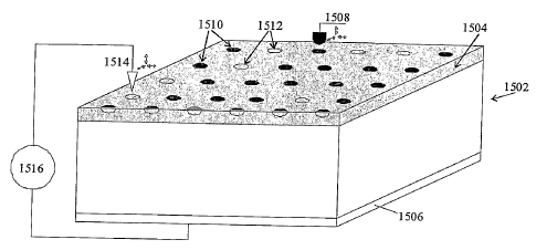
Figure 15 is a schematic diagram of such a memory device in which a piece of
silicon 1502
has a surface layer 1504 of relaxed amorphous silicon. As described above,
this layer 1504
can be created by first forming an unrelaxed amorphous layer by either
deposition or ion
CA 02552958 2006-07-10
WO 2005/057582 PCT/AU2004/001735
-14-
implantation, and then relaxing the amorphous layer using a low temperature
annealing
step (e.g., 450°C for 30 minutes under flowing nitrogen). A metallic
backside contact 1506
provides an electrical contact to the back of the wafer 1502. An indenting
probe 1508 is
used to 'write' bits of binary data by creating crystalline regions 1510
consisting of Si-
III/Si-XII crystalline phases at selected locations on the relaxed amorphous
silicon layer
1504. By controlling the unloading rate of the indenting probe 1508 (e.g., by
ensuring that
the unloading rate is less than 3 mN s i for a 4.2 ~,m radius spherical
indenter tip), the
indented regions are transformed from the relatively electrically insulating
amorphous
phase to a relatively electrically conductive crystalline phase during slow
unloading. In-
situ electrical measurements during indentation of silicon suggest that the
resistivity of the
transformed crystalline and amorphous phases produced by indentation differ by
around an
order of magnitude.
A conducting probe 1514 electrically connected to the back contact 1506 of the
wafer 1502
via a power source 1516 can be moved across the surface of the wafer 1502
using a
suitable translation means (not shown), such as a micro-electro-mechanical
actuator based
on an electrostatic comb drive, a magnetic actuator, piezoelectric members
and/or a shape-
memory alloy such as TiN, for example. When the probe 1514 is positioned over
the
location of a crystalline (transformed) region 1510, electrical current
generated by the
current source 1516 can easily flow through the conductive crystalline region
1510 to the
underlying silicon 1502, particularly if the thickness of the transformed
conductive
crystalline region 1510 is at least comparable to, and preferably equal to or
greater than,
the thickness of the amorphous layer 1504.
Conversely, when the probe 1514 is positioned over an amorphous (untransformed
or re-
transformed by fast unloading) region 1512, electric current cannot easily
flow through the
relatively insulating amorphous region 1512. 'Thus by detecting differences in
the electrical
conductivity of the surface layer 1504, the state of the region below the
probe 1514 can be
determined in a manner analogous to that used in a scanning tunnelling
microscope (STM)
or an atomic force microscope (AFM). Moreover, by representing one binary
state as an
insulating amorphous region 1512 and the complementary binary state as a
crystalline
CA 02552958 2006-07-10
WO 2005/057582 PCT/AU2004/001735
-15-
conductive region 1510, binary data can be stored by controlling the spatial
distributions of
the amorphous regions 1512 and the crystalline regions 1510 within a
predetermined
distribution of sites (or memory cells), such as a regular array, as shown.
In an alternative embodiment, the thickness and therefore resistance of each
transformed
conductive region is determined by controlling the maximum pressure applied to
the
indenter tip. By selecting a desired resistance value from a fixed number of
possible
resistance values, each region can be used for mufti-bit storage. For example,
by
controlling the pressure applied to a single nanoscale region to select the
resistance of that
region from eight possible resistance values, three bits of information are
effectively stored
in that region.
In one embodiment, a single conducting probe 1514 is moved across the surface
layer
1504, using a micro-electro-mechanical actuator. In an alternative embodiment,
a linear or
rectangular or other shaped array of conducting probes or circuits (not shown)
is used so
that many regions can be read simultaneously. If the number of conducting
probes in the
probe array is the same as the number of memory cells, then the conducting
probe array is
fixed relative to the silicon wafer 1502. Alternatively, if the dimensions of
the conducting
probe array are smaller than those of the cell array, then the conducting
probe array is
mounted to an actuator assembly and is moved relative to the surface of the
wafer 1502 so
that all of the memory cells can be read. The probes need to be cleaned before
use and kept
in a relatively dust-free environment.
In order to erase the contents of the memory cells, the transformed
(crystalline) regions
1510 are re-transformed back into an amorphous state by ~re-indenting with the
indenter~
1508 followed by rapid unloading, as shown in Figure 12. Thus, by re-loading a
memory
cell containing Si-XIIlSi-III, the cell can be transformed to the intermediate
phase Si-II.
Fast unloading from this phase then results in a further phase transformation
back to the a-
Si phase.
CA 02552958 2006-07-10
WO 2005/057582 PCT/AU2004/001735
-16-
In one embodiment, the memory device is a read-write device, and the indenter
1508 is an
integral part of the memory device. The indenter 1508 and the conducting probe
1514 can
be mounted on the same actuator assembly.
Alternatively, a single conducting probe/indenter harder than Si-I can provide
the functions
of the indenter 1508 and the conducting probe 1514. Because the contacting ~
area of the
indenting probe 1508 is of the order of 10 nm in diameter, an indenting force
in the wN
range is sufficient to provide the ~11 GPa required to transform amorphous
silicon into a
crystalline phase.
Alternatively, if the memory device is a read-only device, the indenter 1508
is only needed
to store the binary (or multi-bit) data (for example, during manufacture) and
does not have
to be part of the memory device. An external indenter can be used in this
case.
The lateral dimensions of the memory cells can be as small as desired, subject
to the
physical constraints of the indenter 1508 and the conducting probe 1514 and
electrical
crosstalk between cells. Since AFM (and STM) tips of 10 manometers are
routinely used,
the dimensions of the cells may be limited by the physical dimensions of the
indenter
1508, rather than those of the conducting probe 1514. Accordingly, manometer-
scale
memory cells can be produced when the tip of the indenter 1508 is also of
manometer scale.
For example, Figure 13 shows a load-unload curve 1300 for indentation of Si-I
using an
indenter with a tip radius of only 77 nm.
Solid State Device - ROM
In an alternative embodiment, conductive crystalline regions 1602 are formed
at selected
sites in a layer 1604 of relaxed amorphous silicon over an insulating
substrate 1606 (e.g.,
sapphire), as shown in Figure 16. Thus the surface of the relaxed amorphous
layer 1604
can be considered to incorporate a rectangular array of sites 1602, 1608,
comprising
conductive sites 1602 formed by indentation with slow release, and insulating
sites 1608
where no indentation has been performed. A set of elongated parallel
conductors 1610 is
CA 02552958 2006-07-10
WO 2005/057582 PCT/AU2004/001735
-17-
then formed over all of the sites 1602, 1608. Although only three parallel
conductors 1610
are shown in Figure 16 for clarity, it will be appreciated that in practice
additional
conductors similar to the conductors 1610 would be formed over all of the
sites 1602,
1608. Buried beneath the layer 1604 of relaxed amorphous silicon lies another
set of
elongated parallel conductors 1612, perpendicular to the uppermost conductors
1608, and
over which all of the sites 1602, 1608 have been formed. One of the sets of
conductors, for
example the upper conductors 1610, are used as bitlines, and are hereinafter
referred to as
bitlines 1610. The other set of conductive stripes, i. e., the buried
conductors 1612, are used
as wordlines, and are hereinafter referred to as wordlines 1612.
Accordingly, a selected memory cell 1614 can be addressed by applying a bias
to the
corresponding wordline 1616 and measuring the current flowing along the
corresponding
bitline overlaying the site 1614 and not shown in Figure 16 for clarity. This
current will be
appreciably larger (typically more than an order of magnitude) if the region
defining the
selected cell 1614 has been transformed into crystalline silicon than if the
cell has not been
transformed and remains amorphous.
The structure of Figure 16 can be produced by the following process:
(i) Select a silicon-on-sapphire wafer having a Si surface layer of relatively
low resistivity (< 0.01 S2-cm). Use ion implantation and lithography (i.e.,
masked ion implantation) to amorphize a series of parallel elongated strips
or channels of the Si surface layer down to the underlying sapphire to create
insulating channels, with the remaining crystalline silicon subsequently
defining the conductive buried 1612 strips at step (ii) below;
(ii) remove the implantation mask and then perform a second, shallower
implantation to completely amorphize a surface portion of the silicon layer
and thereby define the amorphous surface layer 1604; this also amorphizes
the surface of each conductive strip defined in step (i), thereby forming the
buried conductive channels 1612 that are used as wordlines;
(iii) anneal the wafer at 450°C for 30 minutes under flowing nitrogen
to relax
the a-Si surface layer 1604;
CA 02552958 2006-07-10
WO 2005/057582 PCT/AU2004/001735
-18-
(iv) selected localised regions 1602 are then indented to form localised
conductive regions 1602 and thereby store data in the amorphous 1604 layer
overlaying the wordlines 1612;
(v) annealing of the wafer may be undertaken to transform the indented
conducting regions to Si-I which is expected to have a higher conductivity;
and
(vi) lithography and metal deposition are then used to form the conductive
bitlines 1610 over the localised crystalline regions 1602 and the remaining
amorphous regions 1608.
It will be apparent that in order to most easily distinguish the electrical
conductivity of the
transformed and untransformed regions, it is preferable that the vertical
thickness or depth
of the transformed conductive crystalline region is equal to or greater than
the thickness of
the amorphous layer 1604. This is dependent on the physical dimensions of the
indenter
and the force applied during indentation, and hence the thickness of the
layers is
determined accordingly.
As described above, a single bit of information can be written by transforming
an
electrically insulating region into an electrically conducting region. The bit
is read by
measuring the electrical conductivity of the region, and in the embodiment of
Figure 15,
the bit can be erased by retransforming the conducting region into an
insulating region, in
this case by re-loading the transformed region with ~11 GPa of pressure and
unloading
rapidly. The embodiment in Figure 16 is a read-only device and can be read by
addressing
each cell using the arrangement of wordlines 1612 and bitlines 1610 as shown.
In yet a further alternative embodiment, charge is stored in selected cells of
an array of
crystalline Si regions made, as above, by indentation. This device operates in
an analogous
way to a MOS structure with the active crystalline cell encapsulated (above
and below) by
an insulating material such as amorphous silicon or Si02, for example.
CA 02552958 2006-07-10
WO 2005/057582 PCT/AU2004/001735
-19-
In yet a fzu~ther embodiment, a memory array device is based on
conductivity.differences
between isolated regions of electrically insulating amorphous silicon in a
layer of
electrically conducting crystalline silicon. The insulating amorphous silicon
regions are
initially formed in a layer of crystalline Si-I by indentation using rapid
unloading. Once
formed, an amorphous region can be re-transformed by re-indenting using slow
unloading
to form one or more conductive crystalline phases.
Although the memory devices described above are based on transformations
between an
amorphous phase and one or more crystalline phases, it will be apparent that
any phase
transformation that can be induced by pressure to change the electrical
conductivity of the
cell material can be alternatively used, and that the material undergoing the
phase
transformation need not be silicon but can be any substance or material that
is capable of
undergoing such a transformation. The substance may be elemental or a compound
substance.
In the memory devices described herein, the physical dimensions of the memory
cells
formed by indentation depend upon the size of the indenter tip. Although the
nanometer-
scale memory cells described above provide memory devices having extremely
high
storage density, millimeter-scale memory cells can be used to provide memory
devices
having relatively low storage densities, but which can be manufactured at a
much lower
cost. Such devices are desirable for use in low cost applications that do not
necessarily
require storage of large amounts of information, such as smart cards or train
tickets, for
example.
Although preferred embodiments of the present invention have been described
above in
terms of memory devices, it will be apparent that the ability to change one or
more
electrical andlor physical properties of one or more regions of a substance by
applying and
removing pressure to those regions is not limited to application in memory
devices, but
may be exploited in a wide variety of applications. In particular, the ability
to controllably
and repeatedly change at least one electrical and/or physical property from a
first value to a
second value and back to the first value can be particularly advantageous.
However, the
CA 02552958 2006-07-10
WO 2005/057582 PCT/AU2004/001735
-20-
processes described herein can also be applied to a substance only during
manufacture to
produce a fixed structure including one or more localised regions having one
or more
properties (which may or may not include an electrical property) that differ
from those of
the substance surrounding those regions. Such an arrangement is referred to
herein as a
structured material. For example, the structured material may be an array of
(possibly
nanoscale) regions of at least one first phase of a substance surrounded by at
least one
second phase of the same substance, such as an array of crystalline regions
surrounded by
an amorphous phase, or vice versa. As the electrical and physical properties
of the
substance may differ between the various phases, it is envisaged that such a
structured
material may be useful in a wide variety of applications, including sensors.
Accordingly, although the preferred embodiments have been described above in
terms of
phase transformations, it will be apparent that any property change that can
result from
applying pressure to and removing pressure from one or more regions of a
substance can
be used to form a structured material or to store information. For example,
alternative
embodiments can be used to produce a structured material having one value for
a particular
property (which need not be an electrical property), with localised regions
having one or
more different values for that property. The localised regions may be on a~
nanoscale.
Accordingly, the substance can be any substance that is capable of undergoing
such a
property change by the application and removal of pressure. The substance may
be an
element or a compound.
Many modifications will be apparent to those skilled in the art without
departing from the
scope of the present invention as herein described with reference to the
accompanying
drawings.